There are 5 output signals, that can perform 3 functions:
OUT1 , OUT2 , (See here below)
HIGH LEVEL SIGNAL (LH) , (See paragraph 3.5)
LOW LEVEL SIGNAL (LL), (See paragraph 3.5)
ERROR.
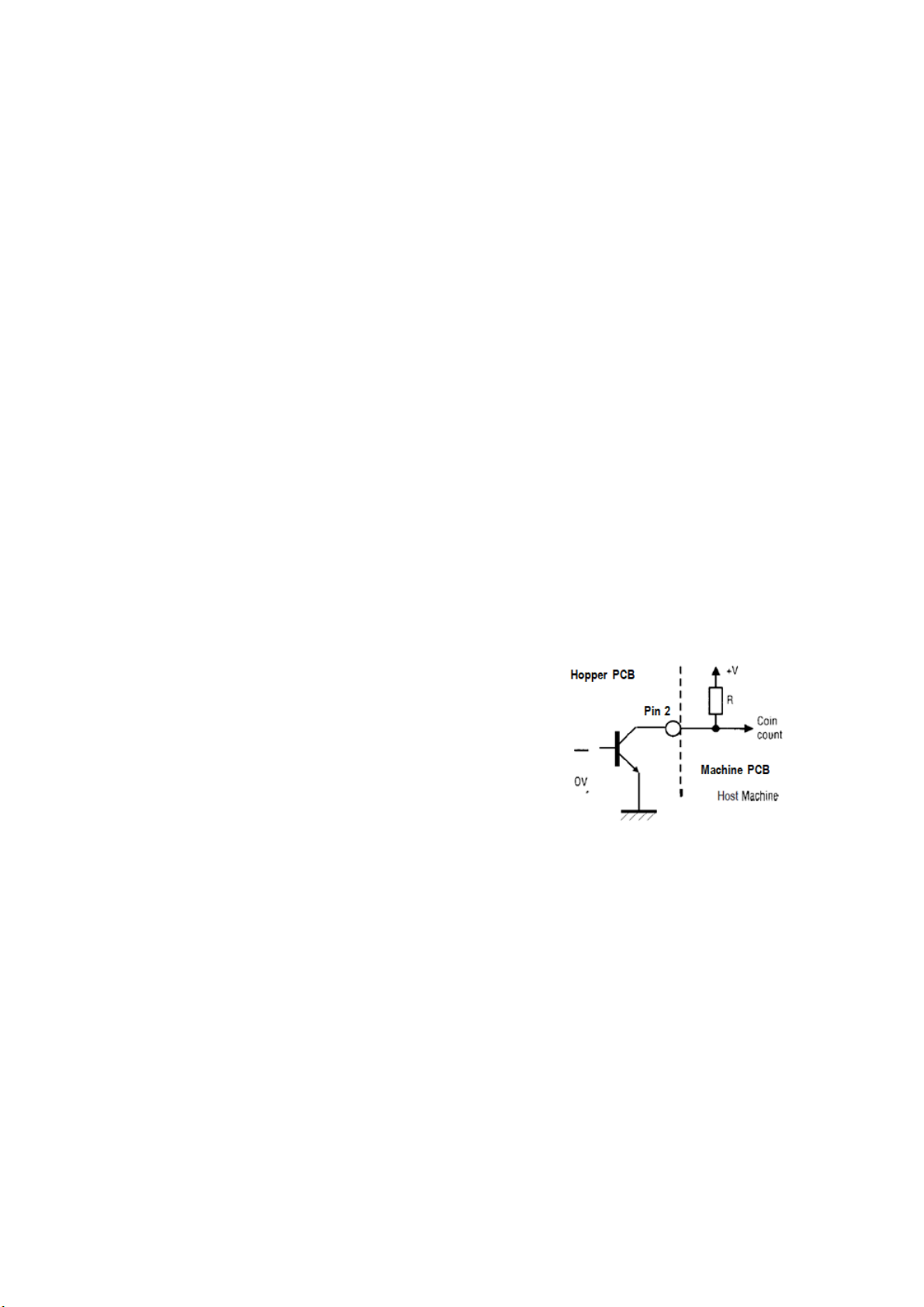
OUT 1 and 2 :
The function performed by these outputs is to communicate (by a low signal) the dispensing of each coin. The
quantity of the impulses sent out is directly proportional to the number of tokens paid out by the hopper.
OUT1 and OUT2 are practically identical: they can be used for sending the return signal to the game pcb, or to
possibly connect a counter or relay.
Such signals are open collector type. When the transistor
is not in conduction, a pull up resistor (not included in the
hopper, it must be provided by the OEM) will pull the
output high (5 V or 12 V or 24 V).
The open collector provides for a simple interface to TTL
and CMOS input devices.
Pin3 corresponds to out1 and pin11 corresponds to out2.
3.5 Level signals
Low level signal (LL) pin 7:
For all those systems where it is important to monitor the level of coins remaining in the hopper, a low level signal is
transmitted as long as there are coins in the hopper, and an high level signal gets triggered as the hopper gets empty
or in reserve.
The high level of the signal is produced by a pull-up resistance, while the low level signal is kept by the presence of
the of the coins, whose metallic body is electrically connected to GND.
High level signal (HL) pin 6:
The same as in previous paragraph, but this time the high level signal corresponds to “coins in the hopper”, whilst the
low level signal corresponds to “empty hopper”.