8. Cut off input signal, when output noise and GAIN VR are minimum, the output noise is less
than-95dBu(Please select the corresponding filter), when the GAIN VR is maximum, the output
noise is less than -78dBu, at the same time, make sure the variations of the waveform are normal
when turning the GAIN VR.
9. Connect OUTPUT to RCH OUT, make sure the RCH output specification is the same as above, and
connect the INPUT to RCH IN; also the RCH output specification is the same as above.
10. Listening Test: Input music signal, set the encoder and adjust the GAIN VR, make sure the volume
can change, and also the treble and bass have corresponding variations; cut off the input signal,
make sure the noise sound is normal, set the encoder, make sure the CLICK NOISE is normal.
Second: Use AP to test
1. Set the encoder to FLAT (encoder setting: 0000), INPUT/OUTPUT, use 1/4 TRS Balanced jack to
connect LCH IN, LCH/RCH OUT, plug in POWER&CLIP LED wires(semi product), the red POWER
LED lights up.
2. Input signal is 1KHZ 0dBu (VP-7724 BAL), make sure INPUT GAIN VR is minimum, the output is
-20+/-2dbu, and distortion<0.03%.
3. Adjust INPUT GAIN VR to maximum, the output is +20+/-2dbu, the distortion<0.01 %( It must select
the corresponding filter when test the distortion).
4. Adjust INPUT GAIN VR, set the output to +6.5~+8.5dbu, make sure the CLIP LED lights up slightly at
the moment.
5. Adjust INPUT GAIN VR, set the output to 0+/-0.2dbu, at the same time, make sure the scale of GAIN
VR at 0dB position.
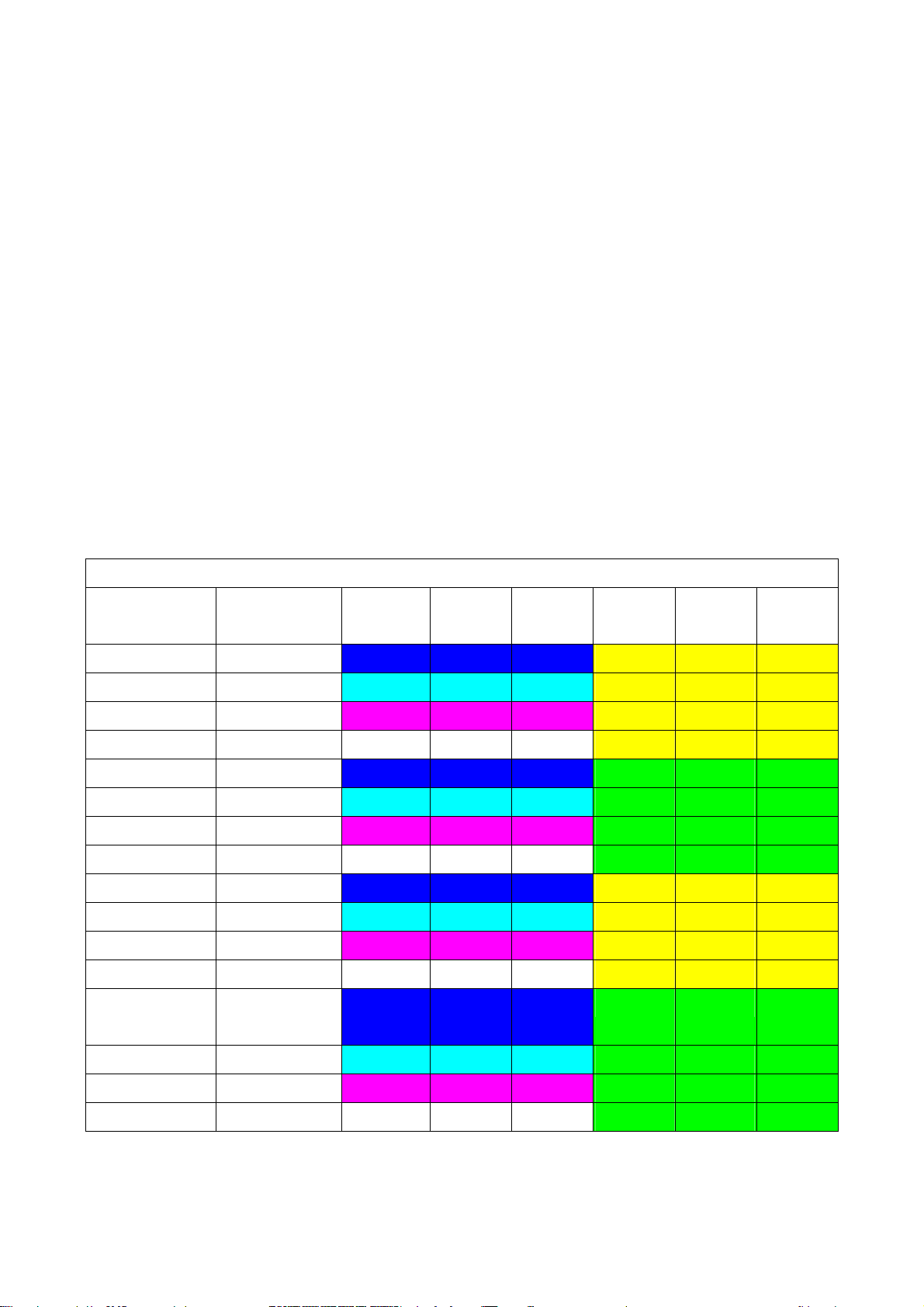
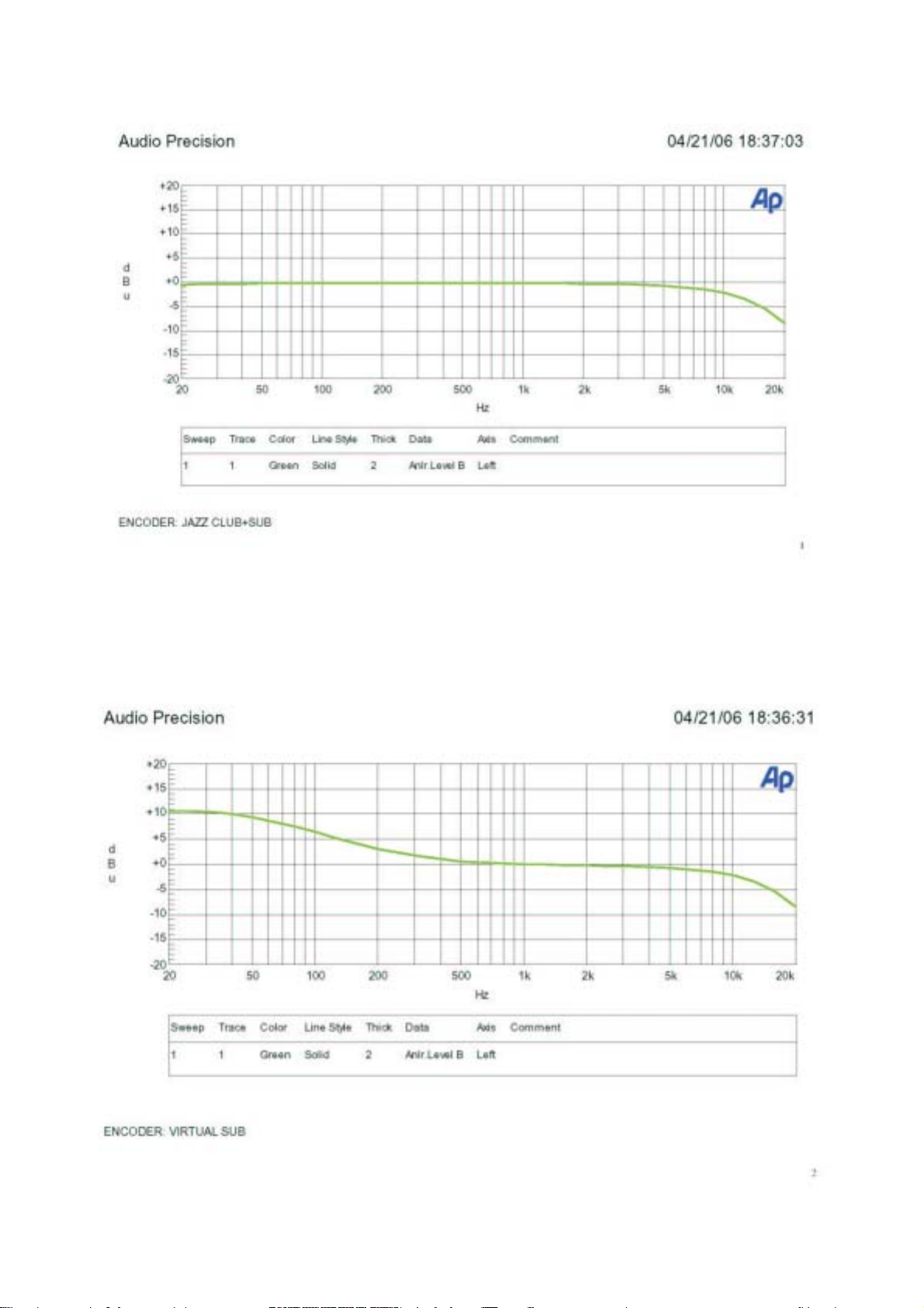
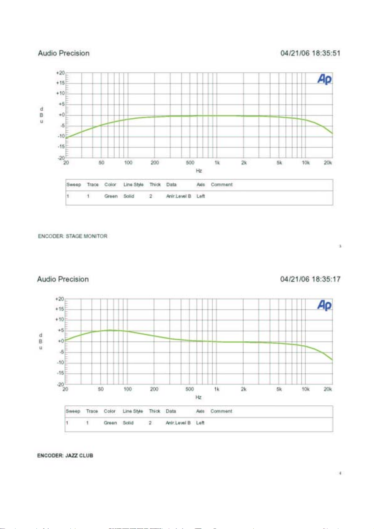
6. According to the following table to test the frequency response, specifications are the following
curves (altogether 4*4=16 modes). In the meantime, make sure the distortion<0.005% under the
FLAT mode.
7. Adjust the input signal to 1 kHz +10dbu, turn GAIN VR from minimum to maximum, and make sure
the distortion will become bigger gradually till clipping (FLAT position).
8. Cut off the input signal, make sure the output noise and GAIN VR are minimum, the output noise is
less than-95dBu (select the corresponding filters), when GAIN VR is maximum, the output noise is
less than -78dBu, at the same time, make sure the variations of the waveform are normal when
turning the GAIN VR.
9. Listening Test: Input music signal, set encoderand adjust the GAIN VR, make sure the volume can
change, and also the treble and bass have the corresponding variation, cut off input signal, make sure
the noise sound is normal, set the encoder,and also make sure the CLICK NOISE is normal.