manuals.online logo
Brands
  1. Home
  2. •
  3. Brands
  4. •
  5. Analog Devices
  6. •
  7. Computer Hardware
  8. •
  9. Analog Devices EVAL-AD7715-5EB User manual

Analog Devices EVAL-AD7715-5EB User manual

One Technology Way, P.O. Box 9106, Norwood. MA 02062-9106, U.S.A.
Tel: 617/329-4700 Fax: 617/326-8703
a
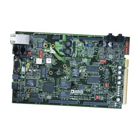
Evaluation Board for
16-Bit Sigma Delta ADC
EVAL-AD7715-5EB
FEATURES
Operates from a Single +5V Supply
On-Board Reference and Digital Buffers
Various Linking Options
Direct Hook-Up to Printer Port of PC
PC Software for Control and Data Analysis
OPERATING THE AD7715-5 EVALUATION BOARD
Power Supplies
The evaluation board has four power supply input pins: AV
DD
,
AGND, DV
DD
and DGND. The AD7715-5 is specified with an
AV
DD
of +5V. Therefore, the AV
DD
voltage supplied to the
board must be +5V. This AV
DD
voltage is also used to power the
AD780 reference. The AD7715-5 can be operated from a +5V
or +3V DV
DD
voltage. When using the 9-way D-type connector
to interface to the evaluation board it is possible to apply a
DV
DD
voltage of either +3V or +5V to the DV
DD
input terminal
on the board. However, when using the 36-way Centronics
connector to interface to the board, the voltage applied to the
DV
DD
input terminal must be +5V. This is because the
Centronics connector is intended for connection to the printer
port of a PC with signals driven from +5V supplies. To run the
board from a single +5V supply, simply connect the AV
DD
and
DV
DD
inputs together.
Both AGND and DGND inputs are provided on the board.
AGND connects to the AD7715-5 AGND pin and also con-
nects to the GND pin of the AD780. DGND connects to the
DGND pin of the AD7715 and to the GND of the digital chips
on the board. The AGND and DGND planes are connected at
the AD7715. Therefore, it is recommended not to connect
AGND and DGND elsewhere in the system to avoid ground
loop problems. When using a single supply for both AV
DD
and
DV
DD
, only one ground connection should be made to the
board. This connection should be made to the board's AGND
input terminal.
Both supplies are decoupled to their respective ground plane
with 10µF tantalum and 0.1µF ceramic disc capacitors.
AD7715
ADC
9-WAY D-TYPE CONNECTOR
36-WAY
CENTRONICS
CONNECTOR
AD780
REFERENCE
AIN(+)
AIN(-)
AVDD AGND DVDD DGND
REF IN
BUFFERS
MCLK IN
INTRODUCTION
This Application Note describes the evaluation board for the
AD7715-5, 16-Bit signal conditioning ADC. The AD7715 is a
complete analog front end for low-frequency applications
providing a fully-differential input channel. The device accepts
low-level signals directly from a transducer and outputs a serial
digital word. It employs a sigma delta technique to realize up to
16 bits of no missing codes performance. Full data on the
AD7715-5 is available in the AD7715 data sheet available from
Analog Devices and should be consulted in conjunction with
this Application Note when using the Evaluation Board.
Included on the evaluation board, along with the AD7715-5, are
an AD780, a +2.5 V ultra high precision bandgap reference, a
2.4576MHz crystal and digital buffers to buffer signals to and
from the edge connectors.
Interfacing to this board is provided either through a 36-Way
Centronics Connector or through a 9-way D-type connector.
External sockets are provided for the analog inputs, an external
reference input option and an external master clock option.
FUNCTIONAL BLOCK DIAGRAM
REV. A
Information furnished by Analog Devices is believed to be accurate and
reliable. However, no responsibility is assumed by Analog Devices for its
use, nor for any infringements of patents or other rights of third parties
which may result from its use. No license is granted by implication or
otherwise under any patent or patent rights of Analog Devices.
EVAL-AD7715-5EB
REV. A–2–
Link Options
There are a number of link options on the evaluation board which should be set for the required operating setup before using the
board. The functions of these link options are described in detail below.
Link No. Function
LK1 This option selects the master clock option for the AD7715. The master clock source comes from the on-board
crystal or from an external clock source via SKT7. This is a double link and both links must be moved together for
correct operation.
With both links in position A, the external clock option is selected and an externally applied clock to SKT 7 is routed
the MCLK IN pin of the AD7715.
With both links in position B, the on-board crystal is selected and provides the master clock for the AD7715.
LK2 This link option is used to select the reference source for the AD7715's REF IN(-) input.
With this link in position A, the REF IN(-) pin of the AD7715 is connected directly to AGND.
With this link in position B, the REF IN(-) pin of the AD7715 is connected to SKT5. An external voltage connected
to SKT5 can now be used for REF IN(-).
LK3 This link option is used to select the reference source for the AD7715's REF IN(+) input.
With this link in position A, the REF IN (+) pin of the AD7715 is connected directly to the output of the on-board
reference, the AD780.
With this link in position B, the REF IN(+) pin of the AD7715 is connected to SKT6. An external voltage connected
to SKT 6 can now be used for REF IN(+).
LK4 This link option is set depending on the type of reference being used on the evaluation board. Although the board is
equipped with an AD780, a REF-192 +2.5V reference can replace it in the same socket. When a REF-192 reference
is used on the board, the link should be in either position A or position B. In position A, the REF-192's shutdown pin
is connected to DV
DD
, placing the REF-192 in normal mode of operation. In position B, the REF-192's shutdown pin
is connected to DGND, placing the REF-192 in power down mode.
When the AD780 reference is used, the link should be in position C as the AD780 does not have a shutdown pin.
LK5 This link is in series with the AIN (+) analog input.
With this link in place, the analog input on the SKT3 input is connected directly to the AIN(+) input on the part.
This link may be removed so that the input signal at SKT3 can be connected to the component grid for signal
conditioning before being applied to the AIN(+) input of the AD7715.
LK6 This link is in series with the AIN (-) analog input.
With this link in place, the analog input on the SKT4 input is connected directly to the AIN(-) input on the part.
This link may be removed so that the input signal at SKT4 can be connected to the component grid for signal
conditioning before being applied to the AIN(-) input of the AD7715.
EVAL-AD7715-5EB
REV. A –3–
Setup Conditions
Table I shows the position in which all the links are set when the
evaluation board is sent out.
Table I. Initial Link Positions
Link No. Position Function.
LK1 B Both links in position B to select the
on-board crystal oscillator as the master
clock for the board.
LK2 A REF IN(-) connected directly to
AGND.
LK3 A REF IN(+) connected to the output of
the on-board AD780 reference.
LK4 C Selects AD780 as the voltage reference.
LK5 IN Connects input signal from SKT3
directly to the AIN(+) pin of the
AD7715.
LK6 IN Connects input signal from SKT4
directly to the AIN(-) pin of the
AD7715.
Figure 2. SKT1 Pin Configuration
2431 5
6789
Table II. SKT1 Pin Designations
1
1 SCLK Serial Clock. The signal on this pin is buffered
before being applied to the SCLK pin of the
AD7715.
2DRDY Logic Output. This is a buffered version of the
signal on the AD7715's DRDY pin.
3CS Chip Select. The signal on this pin is buffered
before being applied to the CS pin of the
AD7715.
4RESET Reset Input. The signal on this pin is buffered
before being applied to the RESET pin of the
AD7715.
5 DIN Serial Data Input. Data applied to this pin is
buffered before being applied to the AD7715's
DIN pin.
6 DGND Ground reference point for digital circuitry.
Connects to the DGND plane on the evaluation
board.
7 DOUT Serial Data Output. This is a buffered version of
the signal on the AD7715's DOUT pin.
8DV
DD
Digital Supply Voltage. The DV
DD
voltage for
the evaluation board can be supplied via this pin
provided no voltage is applied to the main DV
DD
terminal.
9 NC No Connect. This pin is not connected on the
evaluation board.
NOTE
1
An explanation of the AD7715 functions mentioned here is given in Table III as
part of the SKT2 pin designations description.
EVALUATION BOARD INTERFACING
Interfacing to the evaluation board is either via a 9-way D-Type
connector, SKT1, or a 36-way Centronics connector, SKT2.
The pinout for the SKT1 connector is given in Figure 1 and its
corresponding pin designations are given in Table II. The
pinout for this SKT2 connector is shown in Figure 2 and its pin
designations are given in Table III. The evaluation board should
be powered up before a cable is connected to either of the
connectors.
SKT2 is used to connect the evaluation board to the printer
port (parallel port) of a PC. Connection between the two is
direct via a standard parallel printer port cable. SKT1 is used to
connect the evaluation board to any other system.
EVAL-AD7715-5EB
REV. A–4–
118
1936
Figure 3. SKT2 Pin Configuration
Table III. SKT2 Pin Designations
1 NC No Connect. This pin is not connected on the evaluation board.
2 DIN Serial Data Input. Data applied to this pin is buffered before being applied to the AD7715's DIN pin. The
serial data applied to the DIN pin is written to the input shift register on the part. Data from this input shift
register is transferred to the communications register or setup register depending on the register selection
bits of the Communications Register.
3RESET Reset Input. The signal on this pin is buffered before being applied to the RESET pin of the AD7715.
RESET is an active low input which resets the control logic, interface logic, calibration coefficients, digital
filter and analog modulator of the part to power-on status.
4CS Chip Select. The signal on this pin is buffered before being applied to the CS pin of the AD7715. CS is an
active low logic input used to select the AD7715. With this input hard-wired low, the AD7715 operates in its
three-wire interface mode with SCLK, DIN and DOUT used to interface to the device. CS can be used to
select the device in systems with more than one device on the serial bus or as a frame synchronisation signal
in communicating with the AD7715.
5 SCLK Serial Clock. The signal on this pin is buffered before being applied to the SCLK pin of the AD7715. An
external serial clock is applied to this input to access serial data from the AD7715. This serial clock can be a
continuous clock with all data transmitted in a continuous train of pulses. Alternatively, it can be a non-con-
tinuous clock with the information being transmitted to the AD7715 in smaller batches of data.
6-8 NC No Connect. These pins are not connected on the evaluation board.
9DV
DD
Digital Supply Voltage. This provides the supply voltage for IC4, the buffer chip which buffers the output
signals from the AD7715 before they are applied to SKT2.
10 DRDY Logic output. This is a buffered version of the signal on the AD7715's DRDY pin. A logic low on the DRDY
output indicates that a new output word is available from the AD7715 data register. The DRDY pin will
return high upon completion of a read operation of a full output word. If no data read has taken place, after
an output update, the DRDY line will return high for 500* t
CLK IN
cycles prior to the next output update.
This gives an indication of when a read operation should not be attempted to avoid reading from the data
register as it is being updated. DRDY is also used to indicate when the AD7715 has completed its on-chip
calibration sequence.
11-12 NC No Connect. These pins are not connected on the evaluation board.
13 DOUT Serial Data Output. This is a buffered version of the signal on the AD7715's DOUT pin. Serial data from
the output shift register on the part is clocked out on this pin. This output shift register can contain informa-
tion from the communications register, setup register or data register depending on the register selection bits
of the Communications Register.
14-18 NC No Connect. These pins are not connected on the evaluation board.
19-30 DGND Ground reference point for digital circuitry. Connects to the DGND plane on the evaluation board.
31-36 NC No Connect. These pins are not connected on the evaluation board.
EVAL-AD7715-5EB
REV. A –5–
SOCKETS
There are seven sockets on the AD7715-5 evaluation board.
The function of these sockets is outlined in Table IV.
Table IV. Socket Functions
Socket Function
SKT1 9-Way D-Type Connector which can be used for
digital interfacing to the evaluation board.
SKT2 36-Way Centronics Connector which can be used
for digital interfacing to the evaluation board. This
connector should be used when connecting the
board to the parallel printer port of the PC to use
the evaluation software.
SKT3 Sub-Minature BNC Connector. The analog input
signal for the AIN(+) input of the AD7715 is
applied to this socket.
SKT4 Sub-Minature BNC Connector. The analog input
signal for the AIN(-) input of the AD7715 is
applied to this socket.
SKT5 Sub-Minature BNC Connector. The reference
voltage for the REF IN(-) input of the AD7715 is
applied to this socket when the board is configured
for an externally-applied reference voltage.
SKT6 Sub-Minature BNC Connector. The reference
voltage for the REF IN(+) input of the AD7715 is
applied to this socket when the board is configured
for an externally-applied reference voltage.
SKT7 Sub-Minature BNC Connector. The master clock
signal for the MCLK IN input of the AD7715 is
applied to this socket when the board is configured
for an externally-applied master clock.
RUNNING THE AD7715 INTERFACE SOFTWARE
Included in the evaluation board package is a PC-compatible
disk which contains software for controlling and evaluating the
performance of the AD7715 using the printer port of a PC.
There are a total of thirteen files on the distribution disk.
To use the software, the user must have an IBM-compatible PC
and Windows 3.1 must be installed. Start Windows and, using
either the RUN command or the file manager, start the program
called SETUP.EXE on the distribution disk. This automatically
installs the application and sets up a window called ANALOG
DEVICES. The application ICON is found here. To start the
application, double click on the ICON.
When the program stsrts, the user is asked to select a printer
port. The correct selection depends on what type of computer is
being used (Desktop, Laptop etc). LPT1 works for most
machines. When using a Compaq laptop, select PRN. A
different port can be selected at any time from the MAIN
MENU.
The evaluation software does not allow another application
running under Windows to access the printer port while it is
running. Control of the printer port is returned when the
application is quit.
EVAL-AD7715-5EB
REV. A–6–
SCLK
DGND
AGND
AIN(+)
AIN (-)
5
16
11
7
8
6
10
DD
AV DD
15
DV
DD
DVDD
REF IN(+) 9
LK3
AB
SKT6
6
2
4
AD780/
IC2
REF IN(-) 10 BA
SKT5
AD7715
IC1
MCLK OUT 3
LK1
AB
MCLK IN 2AB
SKT7
XTAL1
1
12
DRDY
DIN 14
13 4
CS
DOUT
IC3
74HC4050
C8
C7
C5
10µF C6
0.1µF
C3
10µF C4
0.1µF
C1
10µF C2
0.1µF
AVDD
C12
0.1µF
R1
R2
SW 1 RESET
R6 10kΩ
SKT1
SCLK
CS
DOUT
DIN
DRDY
DGND
6
8
1
3
7
2
5
RESET
4
DV DD
32
10
11 12
14 15
67
9
8
1
C10
0.1µF
C14 C13
3
LK4
C
B
REF-192
D2
4
CS
D0
2
DIN 3
D1
RESET
D3
5
SCLK
36 PIN CENTRONICS CONNECTOR
ACK
DRDY
10 SLCT
13
DOUT
GND
19 - 30
DGND DVDD
D7
7
14
IC4
74LS08
11
1213
3
21
IC5
74LS244
811
12
6
914
4
16 1
19
C11
0.1µF
20
R3
R5 10kΩ
R4 3.3kΩ
D2
HP 5082- 2810
10
5V
SKT 2
C9
0.1µF
LK 6
LK 5
SKT3
SKT4
AV
DGND
AGND
D1
HP 5082- 2810
9
DVDD
A
LK2
Figure 3. AD7715-5 Evaluation Board Circuit Diagram
EVAL-AD7715-5EB
REV. A –7–
COMPONENT LISTING AND MANUFACTURERS
Intergrated Circuits
Component Location Vendor
AD7715 IC1 Analog Devices
AD780 IC2 Analog Devices
74HC4050 IC3 Philips
74LS08 IC4 Texas Instruments
74LS244 IC5 Texas Instruments
HP 5082-2810 D1 & D2 Hewlett Packard
Capacitors
Component Location Vendor
10µF ±20% Tantalum (16 V) C1, C3, C5 AVX- Kyocera
Mftrs No TAG106MO16
0.1µF Ceramic(X7R ±20%) C2, C4, C6, C9, Philips
C10, C11 Mftrs No. CW20C 104M
33pF ±2% Ceramic C13, C14 Philips
Mftrs No. 683 34339
Open Circuit C7, C8,
Resistors
Component Location Vendor
10kΩ±5% 0.25W
Carbon Film Resistor R5, R6 Bourns
3.3kΩ±5% 0.25W
Carbon Film Resistor R4 Bourns
1MΩ±5% 0.25W
Carbon Film Resistor R3 Bourns
Short Circuits R1, R2
Link Options
Component Location Vendor
Pin Headers Lk1 (4x2 way) Harwin
Lk2, Lk3 Mftrs No. M20-9993606
( 2x2 way)
Lk4
(3x2 way)
Lk5, Lk16
(1x2 way)
Shorting Plugs Pin Headers Harwin
(7 required) Mftrs No. M7571-05
EVAL-AD7715-5EB
REV. A–8–
Switch
Component Location Vendor
Push Button Switch SW1 Omron
Mftrs No. B3F1000
Sockets
Component Location Vendor
Miniature BNC Connectors SKT3 - SKT 7 M/A - Com Greenpar
Mftrs No. C65N07G999X99
9-Way D-Type Connector SKT1 McMurdo
Mftrs No. SDE9PNTD
36 Way Centronics Connector SKT 2 Fujitsu
Mftrs No. FCN785J036G0
16-Pin IC Socket IC1 Harwin
8 Pin IC Socket IC2 Mftrs No. D28xx-01
16-Pin IC Socket IC3 xx = No. of Pins
14- Pin IC Socket IC4
20-Pin IC Socket IC5
Wire Wrap Pins DGND, AGND, AVDD, Bicc Vero
DVDD Mftrs No. 663472C
Crystal Oscillator
Component Identification Location Vendor
2.4576MHz Oscillator Xtal 1 IQD
Mftrs No. A166C

This manual suits for next models

1

Other Analog Devices Computer Hardware manuals

Analog Devices ADSP-2181 User manual

Analog Devices

Analog Devices ADSP-2181 User manual

Analog Devices ICE-100B User manual

Analog Devices

Analog Devices ICE-100B User manual

Analog Devices Blackfin User manual

Analog Devices

Analog Devices Blackfin User manual

Analog Devices AD9739 User manual

Analog Devices

Analog Devices AD9739 User manual

Analog Devices ADT7473 User manual

Analog Devices

Analog Devices ADT7473 User manual

Analog Devices EZ-Board ADSP-21489 User manual

Analog Devices

Analog Devices EZ-Board ADSP-21489 User manual

Analog Devices MAX77831 User manual

Analog Devices

Analog Devices MAX77831 User manual

Analog Devices Blackfin ADSP-BF537 Application guide

Analog Devices

Analog Devices Blackfin ADSP-BF537 Application guide

Analog Devices ADICUP3029 User manual

Analog Devices

Analog Devices ADICUP3029 User manual

Analog Devices EVAL-ADAU1860 User manual

Analog Devices

Analog Devices EVAL-ADAU1860 User manual

Analog Devices AD5100 User manual

Analog Devices

Analog Devices AD5100 User manual

Analog Devices ADSP-2186 User manual

Analog Devices

Analog Devices ADSP-2186 User manual

Analog Devices Linear ADI Power LTC3310-1 User manual

Analog Devices

Analog Devices Linear ADI Power LTC3310-1 User manual

Analog Devices ADuCM322 User manual

Analog Devices

Analog Devices ADuCM322 User manual

Analog Devices ADPA1105-EVALZ User manual

Analog Devices

Analog Devices ADPA1105-EVALZ User manual

Analog Devices EVAL-ADN4650EB1Z User manual

Analog Devices

Analog Devices EVAL-ADN4650EB1Z User manual

Analog Devices EZ-KIT Lite ADSP-21364 User guide

Analog Devices

Analog Devices EZ-KIT Lite ADSP-21364 User guide

Analog Devices Linear ADP5070 Quick setup guide

Analog Devices

Analog Devices Linear ADP5070 Quick setup guide

Analog Devices ADSP-21369 EZ-KIT Lite User manual

Analog Devices

Analog Devices ADSP-21369 EZ-KIT Lite User manual

Analog Devices Linear Technology LTC6953 Quick setup guide

Analog Devices

Analog Devices Linear Technology LTC6953 Quick setup guide

Analog Devices UG-397 User manual

Analog Devices

Analog Devices UG-397 User manual

Analog Devices EVAL-ADAQ8088EBZ User manual

Analog Devices

Analog Devices EVAL-ADAQ8088EBZ User manual

Analog Devices ADT7460 User manual

Analog Devices

Analog Devices ADT7460 User manual

Analog Devices Linear DC2331A-A Quick setup guide

Analog Devices

Analog Devices Linear DC2331A-A Quick setup guide

Popular Computer Hardware manuals by other brands

Keithley DAS-1800ST Series user guide

Keithley

Keithley DAS-1800ST Series user guide

Panasonic WJMPU955 - PROCESSING UNIT - TMU operating instructions

Panasonic

Panasonic WJMPU955 - PROCESSING UNIT - TMU operating instructions

TESSERA FL-850/FG4L Hardware manual

TESSERA

TESSERA FL-850/FG4L Hardware manual

Nexcom NEX 6620A user guide

Nexcom

Nexcom NEX 6620A user guide

Diamond Systems MORPHEUS user manual

Diamond Systems

Diamond Systems MORPHEUS user manual

Auvidea X221-LC Technical reference manual

Auvidea

Auvidea X221-LC Technical reference manual

Renesas QB-RL78G1F user manual

Renesas

Renesas QB-RL78G1F user manual

Omnia Omnia-6EX / EXi Installation and operation manual

Omnia

Omnia Omnia-6EX / EXi Installation and operation manual

YASKAWA PROFIBUS-DP SI-P3 installation manual

YASKAWA

YASKAWA PROFIBUS-DP SI-P3 installation manual

Aaeon AEC-6637 user manual

Aaeon

Aaeon AEC-6637 user manual

Freescale Semiconductor 56F8013 installation guide

Freescale Semiconductor

Freescale Semiconductor 56F8013 installation guide

OMAP OMAP5912 reference guide

OMAP

OMAP OMAP5912 reference guide

DIGISYNTHETIC DS216 instruction manual

DIGISYNTHETIC

DIGISYNTHETIC DS216 instruction manual

Alphacool GPX-N 1080Pro-M11 instruction manual

Alphacool

Alphacool GPX-N 1080Pro-M11 instruction manual

MSI Digital@nywhere-ATSC install guide

MSI

MSI Digital@nywhere-ATSC install guide

Alphacool GPX-N 1060-M07 Armor oc V2 M07 instruction manual

Alphacool

Alphacool GPX-N 1060-M07 Armor oc V2 M07 instruction manual

Digitus eSATA II EXPRESSCARD user guide

Digitus

Digitus eSATA II EXPRESSCARD user guide

National Instruments PC-DIO-24/PnP user manual

National Instruments

National Instruments PC-DIO-24/PnP user manual

manuals.online logo
manuals.online logoBrands
  • About & Mission
  • Contact us
  • Privacy Policy
  • Terms and Conditions

Copyright 2025 Manuals.Online. All Rights Reserved.