bonitron M3460 User manual

Model M3460
Ride-Thru
Voltage Regulator
Customer Reference Manual

Bonitron, Inc.
2
Bonitron, Inc.
Nashville, TN
An industry leader in providing solutions for AC drives.
ABOUT BONITRON
Bonitron designs and manufactures quality industrial electronics that improve the reliability of
processes and variable frequency drives worldwide. With products in numerous industries, and
an educated and experienced team of engineers, Bonitron has seen thousands of products
engineered since 1962 and welcomes custom applications.
With engineering, production, and testing all in the same facility, Bonitron is able to ensure its
products are of the utmost quality and ready to be applied to your application.
The Bonitron engineering team has the background and expertise necessary to design, develop,
and manufacture the quality industrial electronic systems demanded in today’s market. A strong
academic background supported by continuing education is complemented by many years of
hands-on field experience. A clear advantage Bonitron has over many competitors is combined
on-site engineering labs and manufacturing facilities, which allows the engineering team to have
immediate access to testing and manufacturing. This not only saves time during prototype
development, but also is essential to providing only the highest quality products.
The sales and marketing teams work closely with engineering to provide up-to-date information
and provide remarkable customer support to make sure you receive the best solution for your
application. Thanks to this combination of quality products and superior customer support,
Bonitron has products installed in critical applications worldwide.
Bonitron, Inc.
3
AC DRIVE OPTIONS
In 1975, Bonitron began working with AC inverter drive specialists at synthetic fiber plants to
develop speed control systems that could be interfaced with their plant process computers. Ever
since, Bonitron has developed AC drive options that solve application issues associated with
modern AC variable frequency drives and aid in reducing drive faults. Below is a sampling of
Bonitron’s current product offering.
WORLD CLASS PRODUCTS
Undervoltage Solutions
Overvoltage Solutions
Uninterruptible Power for Drives
(DC Bus Ride-Thru)
Voltage Regulators
Chargers and Dischargers
Energy Storage
Braking Transistors
Braking Resistors
Transistor/Resistor Combo
Line Regeneration
Dynamic Braking for Servo Drives
Common Bus Solutions
Portable Maintenance Solutions
Single Phase Power Supplies
3-Phase Power Supplies
Common Bus Diodes
Capacitor Formers
Capacitor Testers
Power Quality Solutions
Green Solutions
12 and 18 Pulse Kits
Line Regeneration

M3460
4
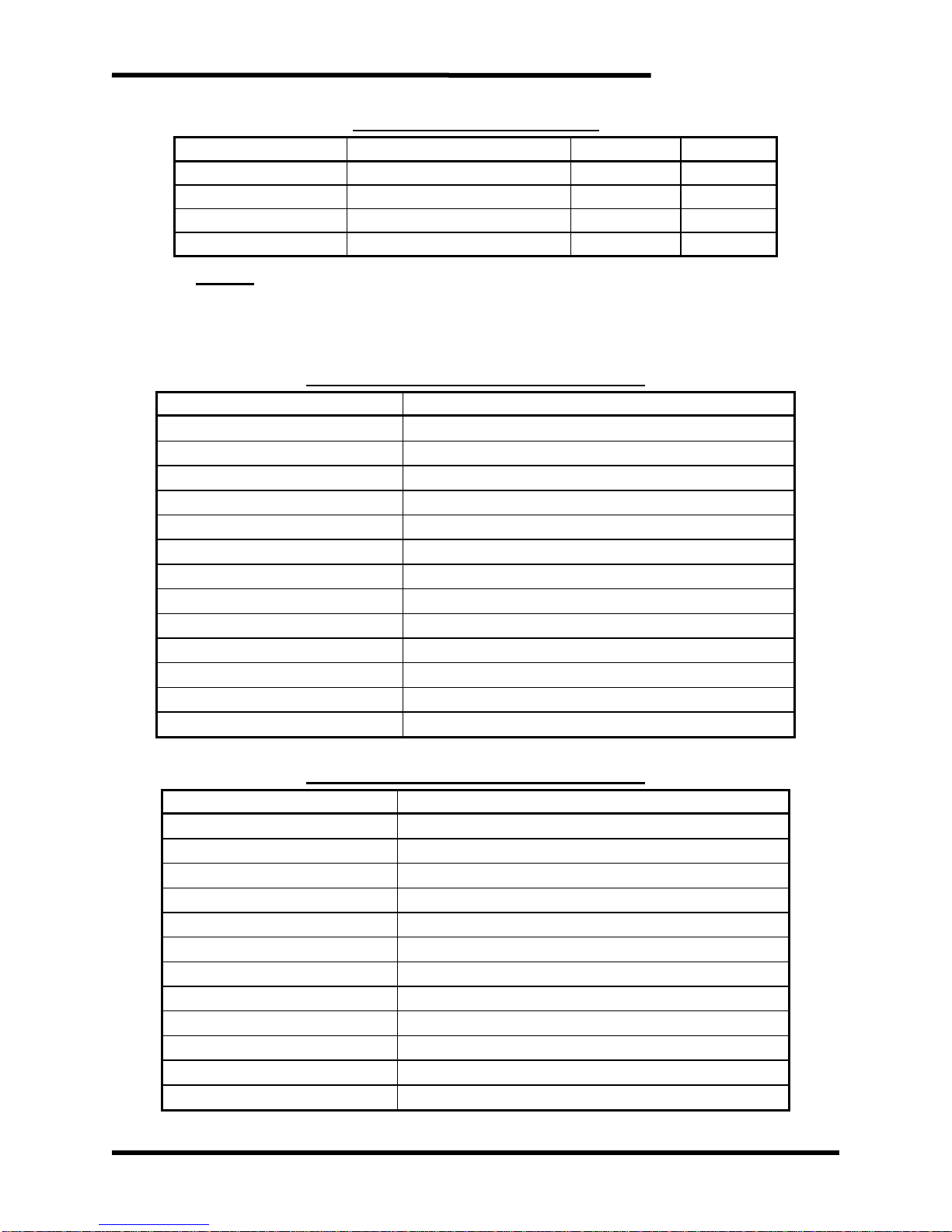
1. INTRODUCTION....................................................................................................................7
1.1. Who Should Use This Manual......................................................................................................7
1.2. Purpose and Scope........................................................................................................................7
1.3. Manual Revision...........................................................................................................................7
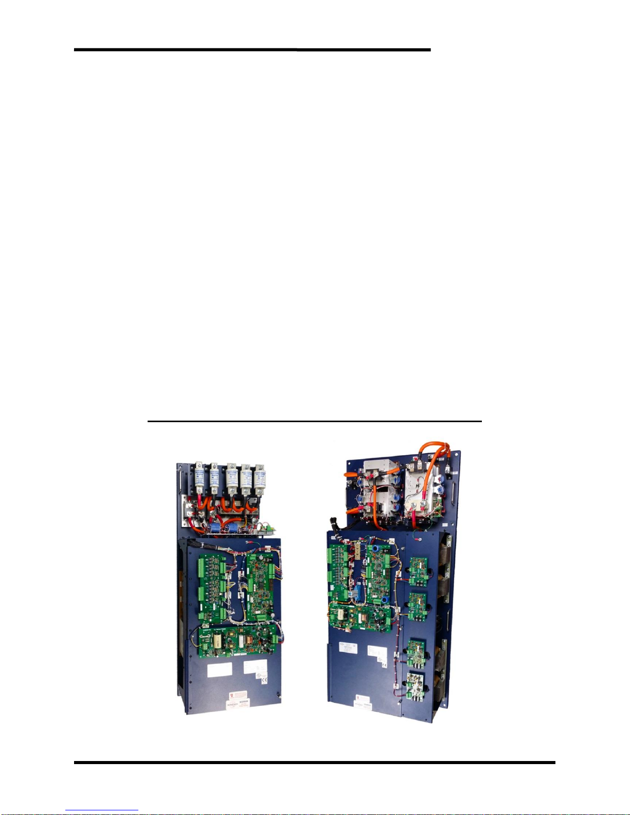
Figure 1-1: M3460R in R11 Chassis and M3460B in R2 Chassis...........................................................7
1.4. Symbol Conventions Used in this Manual and on Equipment.....................................................8
2. PRODUCT DESCRIPTION...................................................................................................9
2.1. Related Products and Documents.................................................................................................9
2.1.1. Products ............................................................................................................................................9
2.1.2. Documents ......................................................................................................................................10
2.2. Part Number Breakdown ............................................................................................................10
Figure 2-1: Example of Part Number Breakdown..................................................................................10
Table 2-1: System Voltage Rating Codes ..............................................................................................10
Table 2-2: Chassis Size Codes ...............................................................................................................11
2.3. General Specifications................................................................................................................11
Table 2-3: M3460R General Specifications...........................................................................................11
Table 2-4: M3460B General Specifications...........................................................................................11
2.4. General Precautions and Safety Warnings .................................................................................12
3. INSTALLATION INSTRUCTIONS ...................................................................................13
3.1. Environment ...............................................................................................................................13
3.2. Unpacking................................................................................................................................... 13
3.3. Mounting ....................................................................................................................................13
3.4. Wiring and User Connections..................................................................................................... 13
3.4.1. Power Wiring..................................................................................................................................13
Table 3-1: M3460R Power Wiring Connections....................................................................................14
Table 3-2: M3460B Power Wiring Connections....................................................................................14
3.4.2. Control Interface and I/O Wiring....................................................................................................15
Table 3-3: User I/O Connections with 3460M6 Board ..........................................................................16
Table 3-4: User I/O Connections with 3660D1 Board...........................................................................17
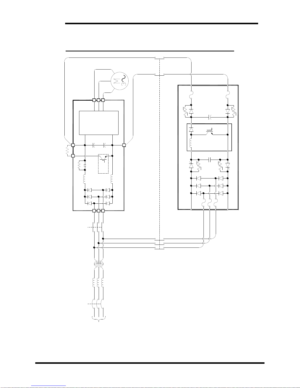
Figure 3-1: M3460 Interconnections with DP10....................................................................................17
3.5. Typical Configurations...............................................................................................................18
Figure 3-2: M3460R Typical Configuration without Energy Storage....................................................18
Figure 3-3: M3460R Typical Configuration with Electrolytic Capacitor Storage Bank........................19
Figure 3-4: M3460R Typical Configuration with Ultracapacitor Storage Bank ....................................20
Figure 3-5: M3460B Typical Configuration with Battery Storage Bank ...............................................21
4. OPERATION .........................................................................................................................23
4.1. Functional Description ...............................................................................................................23
4.2. M3460R Operation for Full Outage Protection..........................................................................23
4.3. Operation Modes and Configuration..........................................................................................23
4.3.1. Normal Operation ...........................................................................................................................23
4.3.2. Test Mode .......................................................................................................................................23
4.4. I/O, Features, and Displays......................................................................................................... 24
Figure 4-1: 3460M6 Status Interface Board Layout...............................................................................24
Figure 4-2: 3460C1 Control Board Layout ............................................................................................24
Figure 4-3: 3460D5 Power Supply Board Layout (for 380V and 460V) ...............................................25
Figure 4-4: 3460D6 Power Supply Board Layout (for 575V)................................................................25
4.4.1. Input Terminals –3460M6 TB7 .....................................................................................................25
Table 4-1: 3460M6 Enable Input Logic Jumper Details........................................................................26
4.4.2. Output Terminals - 3460M6 TB5, TB6 ..........................................................................................26
Table 4-2: 3460M6 Status Output Signal Logic Jumper Details............................................................28

Table of Contents
5
4.4.3. Local I/O Power Supply - TB6 - 1, 9..............................................................................................28
4.4.4. Run Timeout Selection....................................................................................................................28
Table 4-3: Run Timeout Jumper Configurations....................................................................................28
4.4.5. Test Timer Selection.......................................................................................................................29
Table 4-4: Test Timer Jumper Configurations.......................................................................................29
4.4.6. Indicators.........................................................................................................................................29
4.4.7. Fan Timer........................................................................................................................................30
4.4.8. Display Options ..............................................................................................................................30
Table 4-5: Display Panel Configurations ...............................................................................................30
Figure 4-5: Display Panels.....................................................................................................................30
4.5. DC Bus Threshold Voltage Setting............................................................................................32
4.5.1. Determining the DC Bus Threshold Voltage Setting Directly (M3460R Models) .........................32
4.5.2. Determining the DC Bus Threshold Voltage Setting Directly (M3460B Models) .........................33
4.5.3. Determining the DC Bus Threshold Voltage Setting Using the Test Mode....................................33
4.5.4. Adjusting the DC Bus Threshold Voltage Setting ..........................................................................34
4.6. Input Undervoltage (IUV) Level Adjustment.............................................................................34
4.7. Output Undervoltage Level Adjustment.....................................................................................34
5. START-UP, MAINTENANCE AND TROUBLESHOOTING.........................................35
5.1. M3460R Start-up / Field Test Procedure....................................................................................35
5.2. M3460B Start-up / Field Test Procedure....................................................................................36
5.3. Maintenance Items......................................................................................................................37
5.3.1. Capacitor Replacement Recommendations.....................................................................................37
5.3.2. Capacitor Testing Procedure...........................................................................................................38
5.3.3. Cleaning..........................................................................................................................................38
5.3.4. Fans.................................................................................................................................................38
5.3.5. Heatsinks.........................................................................................................................................38
5.4. Troubleshooting..........................................................................................................................39
Table 5-1: Troubleshooting Guide .........................................................................................................39
5.5. Technical Help –Before You Call .............................................................................................40
6. ENGINEERING DATA ........................................................................................................41
6.1. Ratings........................................................................................................................................41
Table 6-1: M3460 kW Ratings...............................................................................................................41
Table 6-2: Factory Setpoints for DC Bus Threshold and Test Boost Voltages......................................41
Table 6-3: M3460R Minimum Input Voltages.......................................................................................41
Table 6-4: M3460B Battery Bank Typical Values.................................................................................41
Table 6-5: M3460R Model Specifications for 230 –480 VAC Systems...............................................42
Table 6-6: M3460B Model Specifications for 230 –480 VAC Systems...............................................42
Table 6-7: M3460R Model Specifications for 575 - 600 VAC Systems................................................43
Table 6-8: M3460B Model Specifications for 575 - 600 VAC Systems................................................43
6.2. Efficiency / Power Consumption................................................................................................43
6.3. Certifications ..............................................................................................................................44
6.3.1. Underwriters Laboratories Listing ..................................................................................................44
6.3.2. CE Conformity................................................................................................................................44
6.3.3. Third Party Certifications................................................................................................................44
6.4. Branch Circuit Protection and Wire Sizing................................................................................44
Table 6-9: M3460R Input Power Wiring Sizes and Fusing ...................................................................45
Table 6-10: M3460B Input Power Wiring Sizes and Fusing .................................................................45
6.5. Dimensions and Mechanical Drawings......................................................................................46
Figure 6-1: M3460-R10 Chassis Dimensional Outline..........................................................................46
Figure 6-2: M3460-R9 Chassis Dimensional Outline............................................................................47
Figure 6-3: M3460-R11 Chassis Dimensional Outline..........................................................................48
Figure 6-4: M3460-R2 Chassis Dimensional Outline............................................................................49
Figure 6-5: DD5 Digital Display Cutout and Mounting Dimensions.....................................................50

M3460
6
Figure 6-6: DP10 Display Cutout and Mounting Dimensions ...............................................................50
7. APPENDICES........................................................................................................................51
7.1. M3460 Installation Considerations.............................................................................................51
7.2. Specifying an Ultracapacitor Storage Bank for Full Outage Protection With M3460R Models 51
7.2.1. Energy Required for Outage ...........................................................................................................53
7.2.2. Minimum Capacitor Bank Voltage .................................................................................................53
7.2.3. Peak Current....................................................................................................................................53
7.2.4. Capacitor Specifications .................................................................................................................53
7.2.5. Minimum Series String ...................................................................................................................54
7.2.6. Available Joules..............................................................................................................................54
7.3. Steering Diode Sharing with a Bonitron M3460 Ride-Thru.......................................................55
Figure 7-1: Diode Sharing Example.......................................................................................................56
7.4. Sag Only Installations & Circulating Currents...........................................................................57
Figure 7-2: M3460R Typical Configuration without Energy Storage....................................................57
Figure 7-3: M3460R Typical Configuration with Current Flow............................................................58
Figure 7-3: M3460R Typical Configuration with Current Flow with affected SCR Highlighted..........59
Figure 7-4: M3460R Typical Configuration with Ultracapacitor Storage Bank ....................................60
User’s Manual
7
1. INTRODUCTION
1.1. WHO SHOULD USE THIS MANUAL
This manual is intendedfor use by anyone who is responsible for integrating, installing,
maintaining, troubleshooting, or using this equipment with any AC drive system.
Please keep this manual for future reference.
1.2. PURPOSE AND SCOPE
This manual is a user’s guide for the model M3460 ride-thru voltage regulator. It will
provide the user with the necessary information to successfully install, integrate, and
use this in a variable frequency AC drive system.
In the event of any conflict between this document and any publication and/or
documentation related to the AC drive system, the latter shall have precedence.
1.3. MANUAL REVISION
Figures 3-2, 3-3, 3-4, and 3-5 were updated in Rev 00d.
Manual template was updated in Rev 00e
Section 7.4 Application Note for Circulation Currents was added in Rev 00f.
Figure 6-5 was updated in Rev 00g
Updates to Section 5.4 and 7.2, and Figure 3-4 were made in Rev 00h.
The display options were updated in Rev 00i.
Updated tables 2-3, 2-4, 6-1, 6-2, 6-3, 6-4 and figures 6-1, 6-2, 6-3 in Rev 00j.
Update to include DD5 display in Rev 01a.
Figure 1-1: M3460R in R11 Chassis and M3460B in R2 Chassis
M3460
8
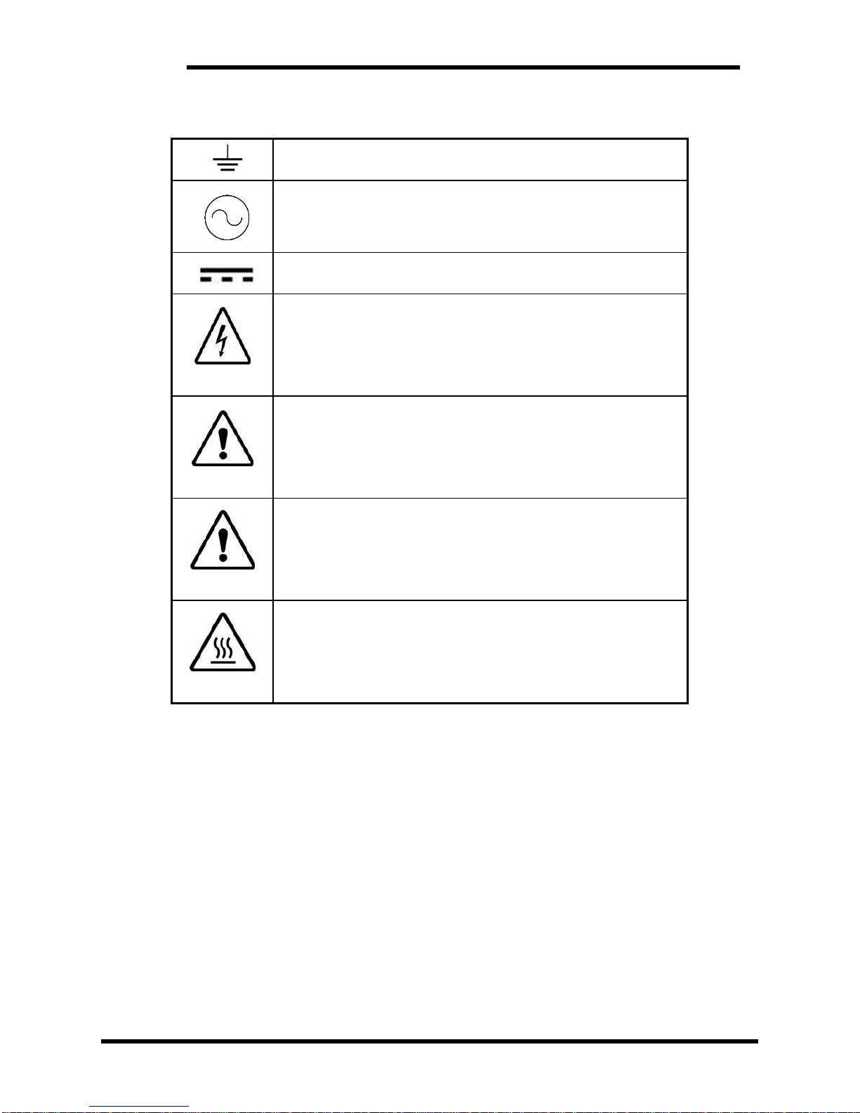
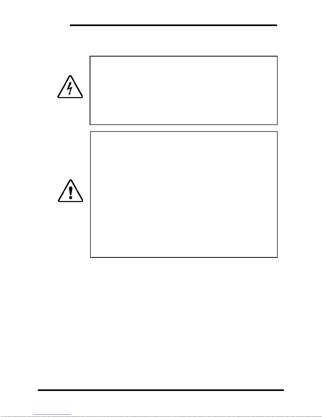
1.4. SYMBOL CONVENTIONS USED IN THIS MANUAL AND ON EQUIPMENT
Earth Ground or Protective Earth
AC Voltage
DC Voltage
DANGER!
DANGER: Electrical hazard - Identifies a statement that indicates
a shock or electrocution hazard that must be avoided.
DANGER!
DANGER: Identifies information about practices or circumstances
that can lead to personal injury or death, property damage, or
economic loss.
CAUTION!
CAUTION: Identifies information about practices or circumstances
that can lead to property damage, or economic loss. Attentions
help you identify a potential hazard, avoid a hazard, and
recognize the consequences.
CAUTION!
CAUTION: Heat or burn hazard - Identifies a statement regarding
heat production or a burn hazard that should be avoided.

User’s Manual
9
2. PRODUCT DESCRIPTION
Bonitron’s M3460 ride-thru voltage regulators provide protection from power quality events
for variable frequency drives (VFDs) that use a fixed rectifier and DC bus. The M3460R
provides sag protection for up to 2 seconds at 50% line sag on all 3 phases. It can also
provide protection from short term full outages of up to 2 seconds with the addition of
storage systems, such as capacitors. The M3460B, in conjunction with a battery bank,
provides full outage protection for up to 4 minutes at full power rating or 15 minutes at
50% power rating during a full outage.
Industries with continuous processes can suffer huge losses from equipment downtime,
loss of production, or damaged product when VFDs trip on under-voltage conditions.
Traditional UPS solutions are connected in series, which decreases the overall drive
system reliability. All Bonitron ride-thru products connect in parallel with the drive, thus
increasing system availability and reliability.
The M3460 regulates incoming voltage to the DC bus of the variable frequency drive. This
allows the drive to “ride through” these events while maintaining motor speed and torque
without experiencing drive shutdown.
ADVANTAGES
•Reliability
•Parallel connection to AC system
•M3460 maintenance can be done while normal process is on-line
•Works with almost any fixed bus, variable frequency, PWM drive
•Only 2-3 parallel connections
•Can use existing AC feed wiring and breakers
•Instant response
•Bumpless transfer
•Easy commissioning
2.1. RELATED PRODUCTS AND DOCUMENTS
2.1.1. PRODUCTS
S3460CR SERIES RIDE-THRU SYSTEMS
Complete systems that use electrolytic capacitor storage for short term power
outages.
S3460UR SERIES RIDE-THRU SYSTEMS
Complete systems that use ultracapacitor storage for short term power
outages.
S3460BR SERIES RIDE-THRU SYSTEMS
Complete systems that use batteries for longer term power outages.
M3534 SERIES RIDE-THRU MODULES
Voltage regulators used for sag or outage protection of lower power systems.
M3528 BATTERY AND ULTRACAPACITOR CHARGERS
Chargers for high voltage storage strings.
M3460
10
2.1.2. DOCUMENTS
Please refer to the KIT 3660DD5 manual when this unit is equipped with the
DD5 Digital Display option. This manual is available at www.bonitron.com or
by contacting Bonitron.
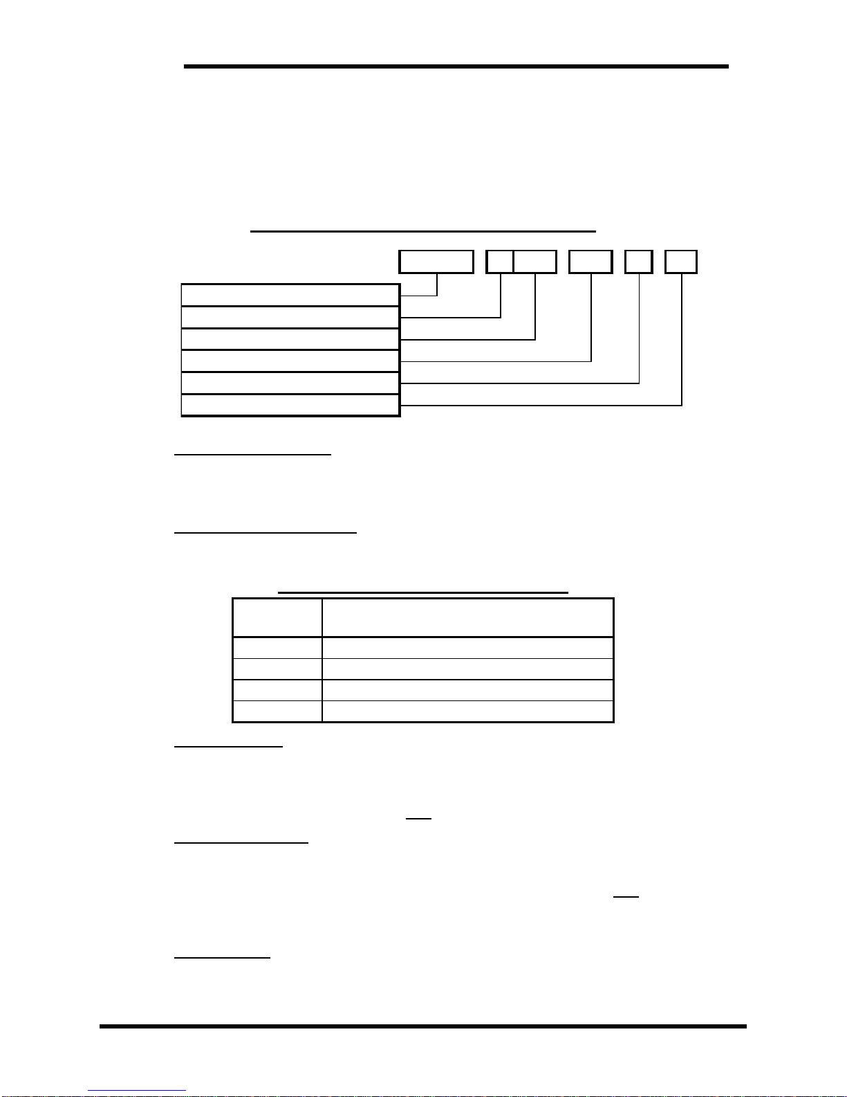
2.2. PART NUMBER BREAKDOWN
Figure 2-1: Example of Part Number Breakdown
- - - -
F
Fusing
SystemVoltage Rating
Power Rating
Outage Duration
Chassis Size
M3460R
H
100
240
R9
Base Model Number
BASE MODEL NUMBER
The base model number for all ride-thru modules in this series rated for 2 second
operation is M3460R. The base model number for all ride-thru modules in this series
rated for 4-15 minute operation is M3460B.
SYSTEM VOLTAGE RATING
The M3460 is available in several input voltage ratings. This rating is indicated by a
code as shown in Table 2-1.
Table 2-1: System Voltage Rating Codes
RATING
CODE
NOMINAL VOLTAGE
(AC LINE /DRIVE BUS)
L
230 VAC / 325 VDC
E
380 - 415 VAC / 540 - 585 VDC
H
460 VAC / 650 VDC
C
575 - 600 VAC / 810VDC
POWER RATING
The power rating indicates the maximum power in kilowatts that can safely be handled
by the M3460 and is represented by a 3-digit value based on the nominal DC system
voltage rating and the maximum output current rating of the M3460. For instance, the
rating code for a 100kW M3460 is 100.
OUTAGE DURATION
The outage duration indicates the amount of time (in seconds) the M3460B module is
able to hold the DC bus at the threshold level while loaded to the rated current. This
duration is directly represented by a 3-digit value. For example, 240 in this position,
represents 240 seconds (4 minutes) of outage duration.
This code is omitted on M3460R models.
CHASSIS SIZE
Four open-backplate chassis sizes are indicated by a code as shown in Table 2-2.
This chassis size is determined by the current rating of the unit.
User’s Manual
11
Table 2-2: Chassis Size Codes
CHASSIS SIZE CODE
DIMENSIONS (H X WX D)
3460R
3460B
R10
28.00” x 16.00” x 13.50”
85-127 A
85 A
R9
34.00” x 16.00” x 13.50”
170 A
127-170 A
R11
44.00” x 15.25” x 13.50”
255-425 A
-
R2
52.00” x 24.00” x 12.50”
-
255-340 A
FUSING
The M3460R comes with internal fusing. This code is omitted on all M3460B models
and M3460R models if internal fusing is not desired.
2.3. GENERAL SPECIFICATIONS
Table 2-3: M3460R General Specifications
PARAMETER
SPECIFICATION
Input AC Voltage
208 –575 VAC
Input DC Voltage
200 –675 VDC
Output DC Voltage
265 –810 VDC
DC Bus Current Rating
85 –425 ADC
Power Rating
25 –305 kW
Inactive Power Consumption
<200W
Duty Cycle (Full Load)
1%
Sag/Outage Duration
2 seconds
Enclosure Rating
Open
Operating Temperature
0 to +40ºC
Storage Temperature
-20 to +65 ºC
Humidity
Below 90% non-condensing
Atmosphere
Free of corrosive gas and conductive dust
Table 2-4: M3460B General Specifications
PARAMETER
SPECIFICATION
Input DC Voltage
200 –675 VDC
Output DC Voltage
265 –810 VDC
DC Bus Current Rating
85–340 ADC
Power Rating
25 –245 kW
Inactive Power Consumption
<200W
Duty Cycle (Full Load)
1%
Sag/Outage Duration
4 minutes at full power or 15 minutes at 50% power
Enclosure Rating
Open
Operating Temperature
0 to +40ºC
Storage Temperature
-20 to+ 65 ºC
Humidity
Below 90% non-condensing
Atmosphere
Free of corrosive gas and conductive dust
M3460
12
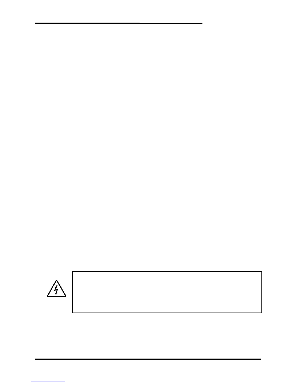
2.4. GENERAL PRECAUTIONS AND SAFETY WARNINGS
DANGER!
•HIGH VOLTAGES MAY BE PRESENT!
•NEVER ATTEMPT TO OPERATE THIS PRODUCT WITH THE
ENCLOSURE COVER REMOVED!
•NEVER ATTEMPT TO SERVICE THIS PRODUCT WITHOUT FIRST
DISCONNECTING POWER TO AND FROM THE UNIT.
•ALWAYS ALLOW ADEQUATE TIME FOR RESIDUAL VOLTAGES TO
DRAIN BEFORE OPENING THE ENCLOSURE.
•FAILURE TO HEED THESE WARNINGS MAY RESULT IN
SERIOUS INJURY OR DEATH!
CAUTION!
•CERTAIN COMPONENTS WITHIN THIS PRODUCT MAY GET HOT
DURING OPERATION.
•ALWAYS ALLOW AMPLE TIME FOR THE UNIT TO COOL BEFORE
ATTEMPTING SERVICE ON THIS PRODUCT.
•INSTALLATION AND/OR REMOVAL OF THIS PRODUCT SHOULD
ONLY BE ACCOMPLISHED BY A QUALIFIED ELECTRICIAN IN
ACCORDANCE WITH NATIONAL ELECTRICAL CODE OR
EQUIVALENT REGULATIONS.
•BEFORE ATTEMPTING INST ALLATION OR REMOVAL OF
THIS PRODUCT ,BE SURE TO REVIEW ALL SYSTEM
DOCUMENTATION FOR PE RTINENT SAFETY
PRECAUTIONS.
•NO USER-SERVICEABLE PARTS ARE CONT AINED
WITHIN THIS PRODUCT.INOPERABLE UNITS SHOU LD BE
REPLACED OR RETURNED F OR REPAIR.
•THIS PRODUCT DOES NOT PROVIDE MOTOR OVERLOAD
PROTECTION.
ANY QUESTIONS AS TO APPLICATION, INSTALLATION, OR SERVICE
SAFETY SHOULD BE DIRECTED TO THE EQUIPMENT SUPPLIER.
User’s Manual
13
3. INSTALLATION INSTRUCTIONS
The M3460 has an open frame construction. It is intended to be part of a larger variable
frequency drive system, and will require different hardware for interconnection based on
the installation. An appropriate enclosure may need to be provided to protect personnel
from contact and the system from damage. The enclosure may also need to protect the
equipment from the installation environment.
Please read this manual completely before designing the drive system or enclosure layout
to ensure all required elements are included.
3.1. ENVIRONMENT
The maximum ambient operating temperature of the M3460 should not exceed 40C.
Temperatures above this can cause overheating during operation.
The standby heat production of the M3460 is quite low, but can generate significant
heat during boosting. This is only of concern with the M3460B models because the
M3460R run time of 2 seconds will not allow the system to reach thermal equilibrium,
and should not cause thermal issues.
Non-condensing, filtered air may be required to cool the system if other components
cause excessive heat buildup in the enclosure.
3.2. UNPACKING
Inspect the shipping crate and M3460 for damage.
Notify the shipping carrier if damage is found.
3.3. MOUNTING
Mounting dimensions can be found in Section 6.5.
1. Lift M3460 backplate off the crate bottom using the 4 handles. Eyebolts
may be installed in the mounting holes for lifting with hooks or chains.
2. Install the module to the backplate. Secure the M3460 backplate to the
rack using the backplate’s ½” diameter mounting holes. Mounting
hardware is not supplied with the M3460. The power input terminals will
be at the top of the installation.
3. If supplied, install the display panel in an appropriate location.
3.4. WIRING AND USER CONNECTIONS
Review this entire section before attempting to wire the M3460.
3.4.1. POWER WIRING
DANGER!
THE M3460CAN HAVE MULTIPLE POWER SOURCES,INCLUDING THE MAIN AC INPUT,
ENERGY STORAGE SYSTEMS AND THE DC CONNECTION TO THE VFD.
ENSURE THAT ALL SOURCES ARE DISCONNECTED AND LOCKED OUT BEFORE
ATTEMPTING SERVICE OR INSTALLATION.
FAILURE TO HEED THESE WARNINGS MAY RESULT IN SERIOUS INJURY
OR DEATH!
This section provides information pertaining to the field wiring connections of
the M3460. Actual connection points and terminal numbers of the AC drive
system will be found in the documentation provided with the drive system.
Be sure to review all pertinent AC drive system documentation as well as the
connection details listed below before proceeding.

M3460
14
Table 3-1: M3460R Power Wiring Connections
TERMINAL
DESIGNATION
FUNCTION
WIRING
SPECIFICATION
CONNECTION
TORQUE
AC Line
L1, L2, L3
AC Input
600 VAC
3/8" stud
150 lb-in
Storage Bus
+ -
DC Input
600 VAC
Existing
Diode / SCR
Check Device
Datasheet
Drive Bus
+ -
DC Output
600 VAC
3/8" stud
150 lb-in
Ground
600 VAC
5/16" stud
75 lb-in
Table 3-2: M3460B Power Wiring Connections
TERMINAL
DESIGNATION
FUNCTION
WIRING
SPECIFICATION
CONNECTION
TORQUE
Storage Bus
+ -
DC Input
600 VAC
3/8" stud
150 lb-in
Drive Bus
+ -
DC Output
600 VAC
3/8" stud
150 lb-in
Ground
600 VAC
5/16" stud
75 lb-in
Main power connections should be made with copper wire; use compression
fitting lugs. Wire sizing should be appropriate for the current being carried.
System ratings are listed in Section 6.1.
M3460 ride-thru units only provide full currents for a limited amount of time.
Therefore, wire heating is not as much a concern as mechanical strength.
3.4.1.1. AC LINE (L1, L2, L3) CONNECTIONS
The AC input to the M3460R can temporarily reach up to 200% of the
normal input current during a power quality event. Size the upstream
current protection devices accordingly, so that the incoming AC will not
be interrupted by the temporary power draw.
During a power quality event, the AC input to the drive will not be drawing
current. Sizing the incoming AC feed to supply both the drive and the
M3460R simultaneously is not necessary. Even though the input current
during a power quality event may be higher than the normal input current,
this temporary overload is allowed by most codes without upsizing the
normal AC feed bus.
Due to the increasedcurrents in the ACfeed during apowerquality event,
the total voltage drop of the incoming AC feed should be considered to
make sure the voltage doesn't dip too low.
If line chokes are to be used in the system, the M3460R must be installed
on the load side of these chokes. This minimizes the possibility of
circulating currents through the M3460R and converter section of the
VFD.
There is no needto connect theAC line to theM3460R if an ultracapacitor
bank is being used.The DC connectionsfrom theultracapacitor bank can
be made to any two of the AC line connections so that the existing fuses

User’s Manual
15
can be used for protection. Please note that one terminal will not be
connected. See Figure 3-4.
3.4.1.2. STORAGE BUS (+ -) CONNECTIONS
If an electrolytic capacitor bank is used with the M3460R, the input can
be attached directly to the diode bus bars marked Storage Bus. External
fusing between the capacitor bank and the M3460R is recommended.
The M3460B battery bank connections are made at the Storage Bus
terminal blocks at the top of the module.
Make sure the polarity is correct for these connections, as failure to do
so can cause severe damage to the system.
DANGER!
FOR SYSTEMS THAT HAVE DC STORAGE,ALWAYS MEASURE DC VOLTAGES AND
FOLLOW PROPER PRECAUTIONS TO ENSURE THEY ARE AT SAFE LEVELS BEFORE
MAKING CONNECTIONS.
3.4.1.3. DRIVE BUS (+ -) CONNECTIONS
The M3460 must have a DC bus connection directly to the DC bus filter
capacitors within the drives. Connections cannot be made through the
braking terminals or with precharge resistors or DC link chokes between
the output of the M3460 and the DC bus capacitors in the drive. Consult
the manufacturers' documentation or contact Bonitron for further
assistance.
Make sure the polarity is correct for these connections, as failure to do
so can cause severe damage to the system.
DANGER!
FOR SYSTEMS THAT HAVE DC STORAGE,ALWAYS MEASURE DC VOLTAGES AND
FOLLOW PROPER PRECAUTIONS TO ENSURE THEY ARE AT SAFE LEVELS BEFORE
MAKING CONNECTIONS.
3.4.1.4. GROUNDING REQUIREMENTS
All units come equipped with a ground stud that is connected to the
module chassis. Ground the chassis in accordance with local codes.
Typically, the wire gauge will be the same as is used to ground the
attached drive.
3.4.2. CONTROL INTERFACE AND I/O WIRING
Control wiring allows for remote enabling, testing, and monitoring of the
M3460. Some I/O is duplicated to allow for isolated monitoring; some have a
mutual common.
When a display system is used, the system status outputs on 3460M6 TB6 are
connected to the display. This leaves the outputs on 3460M6 TB5 available for
remote monitoring.
M3460
16
3.4.2.1. CONNECTIONS FOR BASE CONFIGURATION
Table 3-3: User I/O Connections with 3460M6 Board
3460M6
TERMINAL
FUNCTION
ELECTRICAL
SPECIFICATIONS
WIRE
AWG
TORQUE
INPUTS
TB7 –1
Enable/Disable Input +
24VDC, 20mA
16-12
4.5 lb-in
TB7 –2
Enable/Disable Input -
TB7 –3
Test Input +
TB7 –4
Test Input -
ISOLATED OUTPUTS
TB5 –1 & 2
Ride-Thru Ready (RTR)
250V / 120mA
16-12
4.5 lb-in
TB5 –3 & 4
Overtemperature (OT)
TB5 –5 & 6
Voltage Fault (VF)
TB5 –7 & 8
Fault (FLT)
TB5 –9 & 10
Precharge Complete (PCC)
TB5 –11 & 12
Ride-Thru Active (RTA)
TB5 –13 & 14
Input Undervoltage (IUV)
COMMON OUTPUTS
TB6 –1
Local I/O Supply +
24 VDC, 500 mA
16-12
4.5 lb-in
TB6 –9
Local I/O Supply -
TB6 –2
Precharge Complete (PCC)
250 V / 120 mA
TB6 –3
Voltage Fault (VF)
TB6 –4
Overtemperature (OT)
TB6 –5
Ride-Thru Ready (RTR)
TB6 –6
Ride-Thru Active (RTA)
TB6 –7
Input Undervoltage (IUV)
TB6 –8
Output Common
3.4.2.2. CONNECTIONS WITH DD5DIGITAL DISPLAY
When the KIT 3660DD5 digital display is used, some user connections to
the digital display interface are made on a different module than the
M3460. They are made to the 3660I4 interface module.
Refer to the KIT 3660DD5 manual for operational and functional details.
3.4.2.3. CONNECTIONS WITH DP10 ANALOG DISPLAY
When the M3460 is used with the DP10 analog display, the
interconnections are made through TB6 and TB7 on the 3460M6 board
and TB1 on the 3660D1 board.

User’s Manual
17
Table 3-4: User I/O Connections with 3660D1 Board
3660D1
TERMINAL
FUNCTION
ELECTRICAL
SPECIFICATIONS
WIRE
AWG
TORQUE
TB1 –1
Overtemperature (OT)
15 VDC, 15 mA
16
2.1 lb-in
TB1 –2
Voltage Fault (VF)
TB1 –3
Ride-Thru Active (RTA)
TB1 –4
Ride-Thru Ready (RTR)
TB1 –5
Pre-Charge Complete (PCC)
TB1 –6
Test
TB1 –7
Local I/O Supply -
15 VDC, 50 mA
TB1 –8
Local I/O Supply +
Figure 3-1: M3460 Interconnections with DP10
3660D1
J1 BA
TB4
V+
TB1
3460M6
8
7
6
5
4
3
2
1
COM
TEST
PCC
RTR
RTA
VF
OT
12345678 TB6
910
1234 TB7
1
2
3
4
5
24V+
PCC
VF
OT
RTR
RTA
SIG COM
24V COM
+-+-
M3460
18
3.5. TYPICAL CONFIGURATIONS
Figure 3-2: M3460R Typical Configuration without Energy Storage
FROM THE SAME FEED TRANSFORMER.
CONNECTED DOWNSTREAM.
2. IF LINE CHOKES ARE USED, RIDE-THRU MUST BE
1. INVERTER AND RIDE-THRU SHOULD BE POWERED
~NOTES~
CHOPPER
BRAKING
INTERNAL
VFD
INVERTER
BRAKING
RESISTOR
DISCONNECT
DRIVE
FEED
AC
CHOKES
LINE
GROUND
FAULT
SENSING
DISCONNECT
RIDE-THRU
M3460R
CHOPPER
+
-
+
-
DRIVE
BUS
STORAGE BUS
STORAGE BUS

User’s Manual
19
Figure 3-3: M3460R Typical Configuration with Electrolytic Capacitor Storage Bank
FROM THE SAME FEED TRANSFORMER.
CONNECTED DOWNSTREAM.
2. IF LINE CHOKES ARE USED, RIDE-THRU MUST BE
1. INVERTER AND RIDE-THRU SHOULD BE POWERED
~NOTES~
CHOPPER
BRAKING
INTERNAL
VFD
INVERTER
BRAKING
RESISTOR
DISCONNECT
DRIVE
FEED
AC
CHOKES
LINE
GROUND
FAULT
SENSING
DISCONNECT
RIDE-THRU
M3460R
CHOPPER
+
-
+
-
DRIVE
BUS
STORAGE BUS
STORAGE BUS
RESISTOR
DISCHARGE
ELECTROLYTIC
CAPACITORS
WITH PRECHARGE
ASM 3534EC

M3460
20
Figure 3-4: M3460R Typical Configuration with Ultracapacitor Storage Bank
KIT 3628T
DISCHARGER
M3628R
CHOPPER
BRAKING
INTERNAL
VFD
INVERTER
BRAKING
RESISTOR
DISCONNECT
DRIVE
FEED
AC
CHOKES
LINE
GROUND
FAULT
SENSING
M3528AC CHARGER
ULTRA CAP
ENERGY STORAGE
BANK
DISCONNECT
RIDE-THRU
M3460R
CHOPPER
+
-
+
-
+
-
DRIVE
RIDE-THRU
DISCONNECT
AUX. CONTACT
BUS
STORAGE BUS
STORAGE BUS
M
3
ISOLATION TRANSFORMER
FROM THE SAME FEED TRANSFORMER.
CONNECTED DOWNSTREAM.
2. IF LINE CHOKES ARE USED, RIDE-THRUMUSTBE
1. INVERTER AND RIDE-THRU SHOULD BE POWERED
~NOTES~
+
-
L1
L2
ASM 3460PS
IS LOWER THAN PCC VOLTAGE.
3. ASM 3460 PS WILL BE USED IF THE INPUT DC LEVEL
*OPTIONAL: SEE SECTION 7.2
Other manuals for M3460
1
Table of contents
Other bonitron Controllers manuals


Popular Controllers manuals by other brands

Fuji Electric
Fuji Electric CC-M instruction manual

RCTimer
RCTimer Ares F7 Quick reference manual

Rain Bird
Rain Bird ESP-Me user manual

United Technologies
United Technologies Carrier OPN-VAVB1 Installation and startup guide

Engineered air
Engineered air EngA M-TRAC4 User's operation manual

Chauvet
Chauvet Obey 6 user manual


