ST STEVAL-A6983NV1 User manual

Introduction
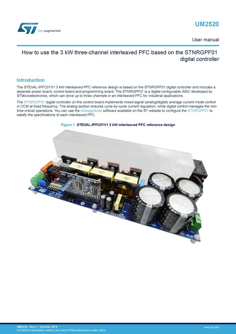
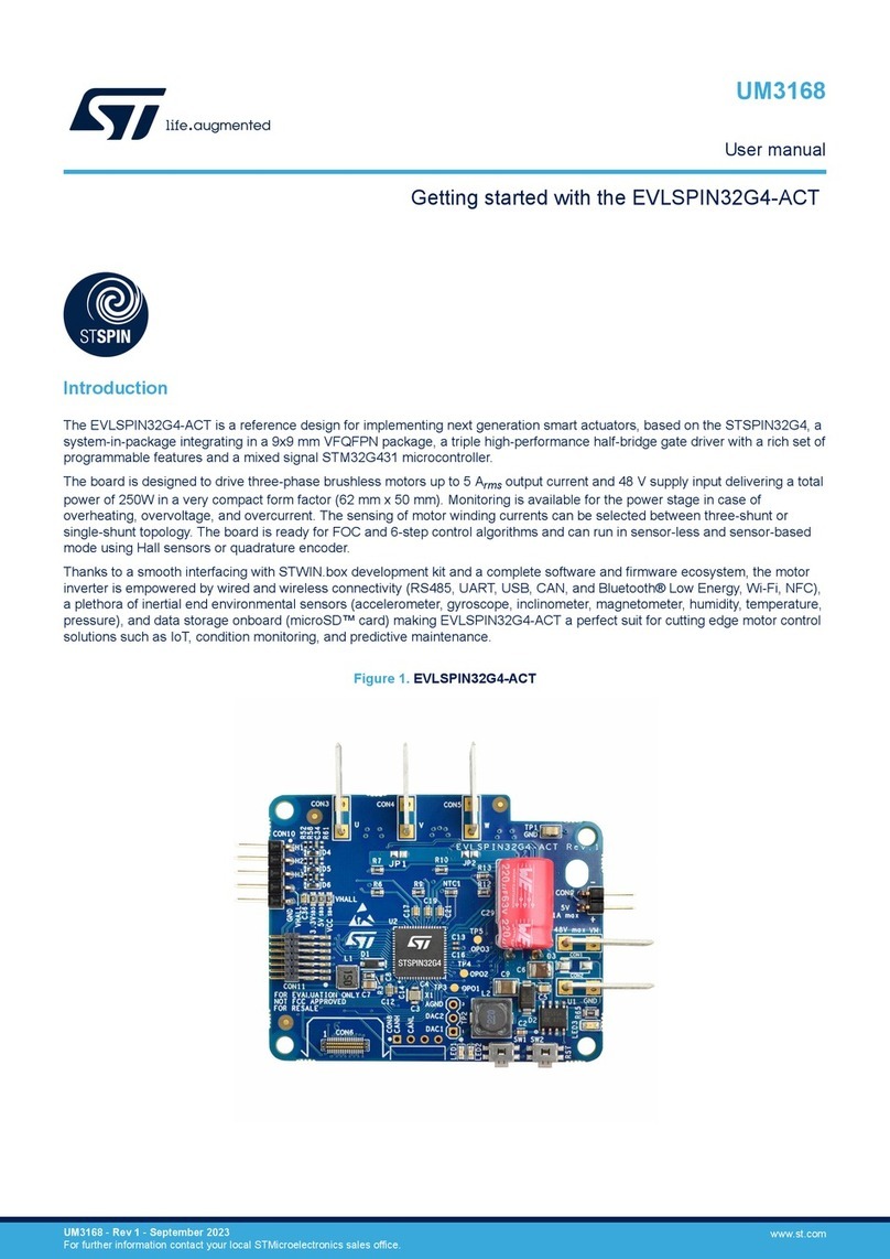
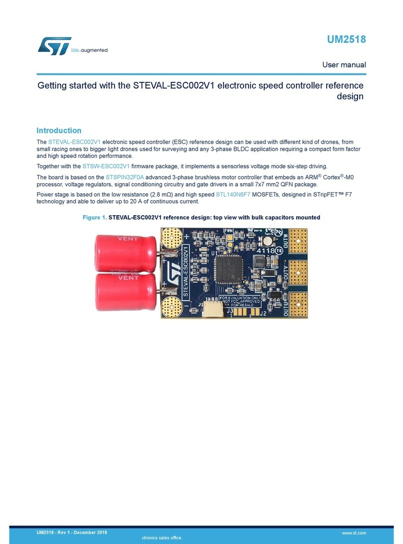
The STEVAL-A6983NV1 is based on the A6983NQTR synchronous step-down regulator, which implements the peak current
mode architecture in a VQFN package with internal compensation, to minimize design complexity and size. The device is able
to deliver up to 3 A DC to the load.
The STEVAL-A6983NV1 operates over an input voltage range of 6 to 38 V to provide a regulated 5 V output at a switching
frequency of 400 kHz.
The board can be easily modified to obtain:
• the preferred switching frequency, modifying the resistor connected to the FSW pin
• the preferred power-up threshold, modifying the resistors partition
• the required output voltage, changing the feedback resistors partition
Use the eDesignSuite software to configure the A6983NQTR and satisfy the specifications.
Figure 1. STEVAL-A6983NV1 evaluation board
Getting started with the STEVAL-A6983NV1 synchronous step-down switching
regulator evaluation board based on the A6983NQTR
UM3094
User manual
UM3094 - Rev 1 - February 2024
For further information contact your local STMicroelectronics sales office. www.st.com

1 Getting started
1.1 Safety precautions
Caution: All operations involving transportation, installation, use, and maintenance of the board must be performed by
skilled technical personnel who is familiar with the installation, use, and maintenance of power electronic
systems.
A system architecture that supplies power to the evaluation board must be equipped with additional control and
protective devices in accordance with the applicable safety requirements (that is, compliance with technical
equipment and accident prevention rules).
The electrical installation has to be completed in accordance with the appropriate requirements (cross-sectional
areas of conductors, fusing, and GND connections).
1.2 Overview
1.2.1 Features
• AEC-Q100 Grade 1 qualified
• Operating temperature range: -40 to +150°C for Tj
• 3.5 to 38 V operating input voltage
• Output voltage from 0.85 V to VIN
• 3.3 and 5 V fixed output voltage versions
• 3 A DC output current
• Internal compensation network
• Noise sensitive applications
• 2 μA shutdown current
• Internal soft-start
• High voltage VIN compatible enable
• Output overvoltage protection
• Output voltage sequencing
• Thermal protection
• 0.2 to 2.2 MHz programmable switching frequency
• Stable with low ESR capacitor min. 22 µF
• Optional spread spectrum for improved EMC
• Power good
• Synchronization with an external clock
• QFN16 (3 x 3 mm) package
1.2.2 Block diagram
Figure 2. STEVAL-A6983NV1 functional block diagram
EMI
filter
Input
filter Output
Switching
regulator filter
Enable/External clock
management
Feedback
network
LOAD
VOUT
DC Input
Enable
Ext. Clock
PGOOD
UM3094
Getting started
UM3094 - Rev 1 page 2/52

1.2.3 Connectors and test points
VIN: connect to the positive terminal of a supply voltage (from 6 V to 38 V with default 5 V VOUT). The input
voltage is filtered (see Section 1.2.4: Input EMI filter) to decrease the EMI. The supply voltage should be set with
a current limitation compatible with the power board request.
Typically:
Ilim >VOUT
VIN ⋅ IOUT
GND: return of the terminal of the input and output capacitors.
VOUT: connect to the positive terminal of the active load or to a power resistor between VOUT and GND.
Important: For all the above connections, short wires are recommended to avoid oscillation between the cable parasitic
inductance and the input capacitor.
CLKIN: input pin. The pin allows synchronizing the device by applying an external signal generator. Refer to the
AC coupling synchronization paragraph of the online datasheet.
GND: signal GND.
EN: input pin. The pin allows enabling the device. It allows also synchronizing the device by applying an external
signal generator. Refer to the DC coupling synchronization paragraph of the online datasheet.
PGOOD: output pin. It is an open collector. It is short to GND once VOUT is lower than the regulator window
(10%). Otherwise, it is short to the VOUT voltage.
1.2.4 Input EMI filter
The STEVAL-A6983NV1 is compliant with CISPR16-4-2.
The suggested input filters help to reduce EMI.
The network consists of a double Pi filter with an inductor (L2), a ferrite bead (L5), MLCC capacitors (C18, C19,
C20 and C30), and an electrolytic capacitor used for a bulk energy storage.
1.2.5 Switching frequency settings
By default, the switching frequency is equal to 400 [Khz]. It is possible to select the preferred switching frequency
by selecting the resistor connected between ground and the RFSW pin, R8.
Table 1. Switching frequency settings
R8 [KΩ] Fsw [MHz]
1.8 0.2
0 0.4
3.3 0.5
5.6 0.7
10 1
18 1.5
33 2
56 2.3
The spread spectrum is selectable by connecting the RFSW resistor to VCC. The internal dithering circuit
changes the switching frequency in a range of ± 5%. Refer to the online datasheet for the spread spectrum full
description.
UM3094
Getting started
UM3094 - Rev 1 page 3/52

1.2.6 EN settings
By default, the EN pin is directly connected to VIN with the R1 resistor and, as soon as the VIN rises over the
UVLO voltage, the device turns on.
By correctly selecting the resistor partition connected to the EN pin, it is possible to program the power-up
threshold:
Vpowerup = 1.2 1 + R1
R2
1.2.7 VOUT settings
By default, the STEVAL-A6983NV1 is with VOUT = 5 V. However, the output voltage can be managed from 0.85 V
to a higher voltage by selecting the right output partition resistors (R3 and R4):
VOUT =R3+R4
R4⋅ VFB
Where: VFB is equal to 0.85 V.
1.2.8 eDesignSuite
The eDesignSuite suite software tool helps you to configure ST products for power conversion applications.
You can use it to customize a PFC controller for a specific application. Start by entering the main specifications for
your design. Then, generate an automatic design or follow a sequential process to build a highly customized
design.
UM3094
Getting started
UM3094 - Rev 1 page 4/52

2 How to use the board
The STEVAL-A6983NV1 is configured with A6983 LNM with adjustable VOUT. The board is set to deliver a 5 V
output voltage with Fsw = 400 KHz.
This board is best suited for applications where the low output ripple is preferred on every load condition.
To use the board, follow the procedure below.
Step 1. Connect the voltage supply between VIN and GND connectors.
Step 2. Connect the load (power resistor or active load) between VOUT and GND connectors.
Note: For Step 1 and Step 2 short wires are recommended.
Step 3. Set the supply voltage VIN from 6 to 38 V.
Step 4. By default, VOUT is set equal to 5 V. Increase or decrease the output power resistor or active load to
reach the suitable output current (max. 3 A).
UM3094
How to use the board
UM3094 - Rev 1 page 5/52

3 Application 1: VOUT = 5 V, FSW = 400 KHz
Application conditions:
• VIN from 6.5 to 38 V
• VOUT = 5 V
• FSW = 0.4 MHz
• IOUT = 3 A
Schematic:
Figure 3. STEVAL-A6983NV1 schematic - application 1
size 1210
C3
10uF
Type = 16V
R9
NM
si ze 1206
0
R12
L1A 15uH
R2
NM
R11
n.m.
Panasonic
EEHZA1H101P 10x10
R13 0.01K
GND TP2
TP1
VIN
R3 400K
C16
1uF
Type = 50V
TP8GND
C17
n.m.
Type = 16V
C8 NM
C4
10uF
Type = 16V
+
C15 100uF 50V
GND
VOUT
EN TP5
VIN
C9
NM
size 1206
C2B
1uF
50V R5
0
VOUT
size 0805
C5
22uF
Type = 16V
size 0603
GND
LX
GND
L1B NM
CLKIN TP6
J2
FB
C11
1uF
Type = 16V
C7 1uF
Type = 16V
TP4
GND
R6
NM
R1
100K
Coilcraft XAL4030
6.8uH L2
GND
size 1206
size 1206
C6
100nF
C14
10uF
Type = 50V
size 0805
U1
A6983
1VIN1
2VINLDO
3SGND1
4EN/CLKIN
PGOOD
5
6VBIAS
FB
7
8FSW
9
VCC
SGND2 10
BOOT 11
VIN2 12
17 EP1-SGND
PGND1 13
SW1 14
SW2 15
PGND2 16
C13
10uF
Type = 50V
C12
10uF
Type = 50V
size 0603
TP3
VOUT
VCC
L3
MPZ2012S221A
C1
10uF
Type = 50V
R7
1Meg
C2A
1uF
Type = 50V
size 1206
size 0805
Coilcraft: MSS1048
Coilcraft: XAL6060
size 0805
EMI filters, optional components
PGOOD TP7
R8
0 Ohm
R4 82k
size 1206
GND
Bill of materials: see Section 10: Bill of materials.
UM3094
Application 1: VOUT = 5 V, FSW = 400 KHz
UM3094 - Rev 1 page 6/52

3.1 Oscilloscope acquisitions for application 1
3.1.1 Power-up from EN
• Yellow = EN
• Green = inductor current
• Blue = VOUT
• Violet = VIN
Figure 4. VIN = 6.5 V; VOUT= 5 V; IOUT = 2 A Figure 5. VIN = 12 V; VOUT= 5 V; IOUT = 2 A
Figure 6. VIN = 24 V; VOUT= 5 V; IOUT = 2 A Figure 7. VIN = 38 V; VOUT= 5 V; IOUT = 2 A
UM3094
Application 1: VOUT = 5 V, FSW = 400 KHz
UM3094 - Rev 1 page 7/52

3.1.2 Power-up from VIN
• Yellow = EN
• Green = inductor current
• Blue = VOUT
• Violet = VIN
Figure 8. VIN = 6.5 V; VOUT= 5 V; IOUT = 2 A Figure 9. VIN = 12 V; VOUT= 5 V; IOUT = 2 A
Figure 10. VIN = 24 V; VOUT= 5 V; IOUT = 2 A Figure 11. VIN = 38 V; VOUT= 5 V; IOUT = 2 A
UM3094
Application 1: VOUT = 5 V, FSW = 400 KHz
UM3094 - Rev 1 page 8/52

3.1.3 VOUT ripple for no load operation
• Green = inductor current
• Blue = VOUT ripple (DC offset = 5 V)
• Violet = switching node
Figure 12. VIN = 6.5 V; VOUT = 5 V; no load; VOUT,
RIPPLE < 10 mV
Figure 13. VIN = 12 V; VOUT = 5 V; no load; VOUT,
RIPPLE < 10 mV
Figure 14. VIN = 24 V; VOUT = 5 V; no load; VOUT,
RIPPLE < 10 mV
Figure 15. VIN = 38 V; VOUT = 5 V; no load; VOUT,
RIPPLE < 10 mV
UM3094
Application 1: VOUT = 5 V, FSW = 400 KHz
UM3094 - Rev 1 page 9/52

3.1.4 VOUT ripple for IOUT = 3 A
• Green = inductor current
• Blue = VOUT ripple (DC offset = 5 V)
• Violet = switching node
Figure 16. VIN = 6.5 V; VOUT = 5 V; IOUT = 3 A; VOUT,
RIPPLE < 10 mV
Figure 17. VIN = 12 V; VOUT = 5 V; IOUT = 3 A; VOUT,
RIPPLE < 10 mV
Figure 18. VIN = 24 V; VOUT = 5 V; IOUT = 3 A; VOUT,
RIPPLE < 10 mV
Figure 19. VIN = 38 V; VOUT = 5 V; IOUT = 3 A; VOUT,
RIPPLE < 15 mV
UM3094
Application 1: VOUT = 5 V, FSW = 400 KHz
UM3094 - Rev 1 page 10/52
Table of contents
Other ST Controllers manuals

ST
ST STEVAL-IAS001V1 User manual
ST
ST STM8AF6223 User manual
ST
ST ST7735R User manual
ST
ST P-NUCLEO-IHM001 User manual
ST
ST STM32F101xx series Owner's manual

ST
ST STEVAL-IHM037V1 User manual

ST
ST STM32W-SK User manual
ST
ST ST5-Q User manual
ST
ST STM32F101xx series User manual
ST
ST STM32MP13-ETZPC User manual
Popular Controllers manuals by other brands
Digiplex
Digiplex DGP-848 Programming guide
YASKAWA
YASKAWA SGM series user manual
Sinope
Sinope Calypso RM3500ZB installation guide
Isimet
Isimet DLA Series Style 2 Installation, Operations, Start-up and Maintenance Instructions
LSIS
LSIS sv-ip5a user manual
Rockwell Automation
Rockwell Automation 1769-L31 installation instructions
