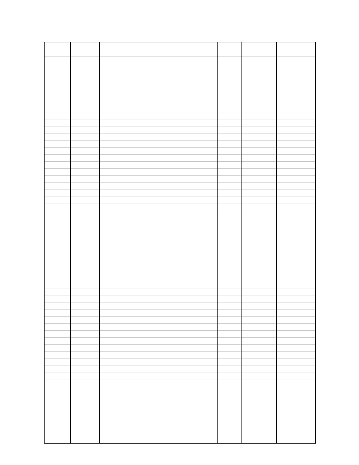
— 5 —
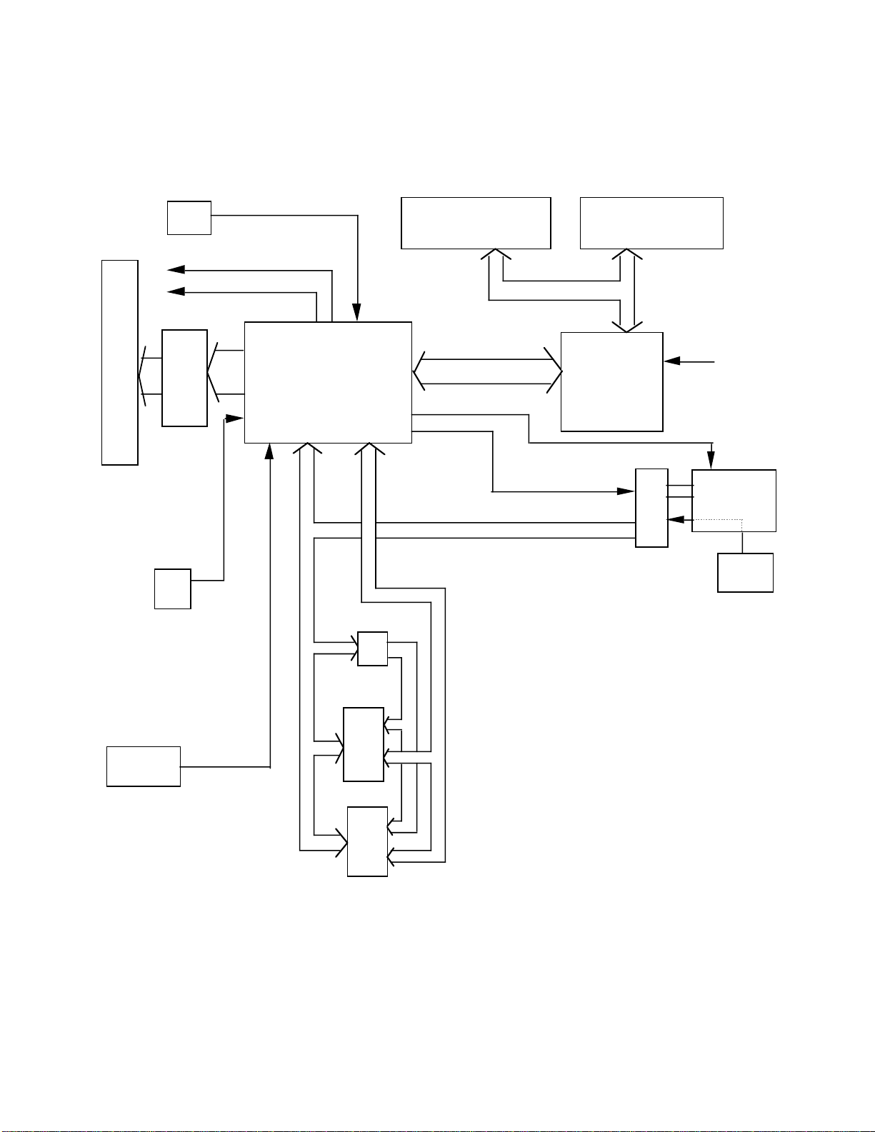
Pin No. Signal Description In/Out Status of
Power On Status of
Power OFF
1 FB3 Not used — — —
2 FB4 RAM bank 3 Out High High
3 FB5 RAM bank 4 Out High High
4 AVSS GND — GND GND
5 PGM Not used — — —
6 RAM Chip select signal for RAM Out High Low
7 AVREF VDD — 5 V 5 V
8 RXD Receive data In High High
9 TXD Send data Out High High
10 WD Winder motor drive signal Out Low Low
11 DI Data signal from uPD16312 In Pulse High
12 DO Data signal to uPD16312 Out Pulse High
13 CLK Clock signal for uPD16312 Out Pulse High
14 STB Data strobe signal for uPD16312 Out Pulse High
15 KC0 Key common signal (KC0) Out Pulse High
16 KC1 Key common signal (KC1) Out Pulse High
17 KC2 Key common signal (KC2) Out Pulse High
18 KC3 Key common signal (KC3) Out Pulse High
19 AD0 Address / Data signal (AD0) In/Out Pulse High
20 AD1 Address / Data signal (AD1) In/Out Pulse High
21 AD2 Address / Data signal (AD2) In/Out Pulse High
22 AD3 Address / Data signal (AD3) In/Out Pulse High
23 AD4 Address / Data signal (AD4) In/Out Pulse High
24 AD5 Address / Data signal (AD5) In/Out Pulse High
25 AD6 Address / Data signal (AD6) In/Out Pulse High
26 AD7 Address / Data signal (AD7) In/Out Pulse High
27 A8 Address signal (A8) Out Pulse High
28 A9 Address signal (A9) Out Pulse High
29 A10 Address signal (A10) Out Pulse High
30 A11 Address signal (A11) Out Pulse High
31 A12 Address signal (A12) Out Pulse High
32 A13 Address signal (A13) Out Pulse High
33 VSS GND — GND GND
34 A14 Address signal (A14) Out Pulse High
35 A15 Address signal (A15) Out Pulse High
36 INIT PAD2 status — — —
37 VPP PAD1 status — — —
38 DSR Data set ready signal In High High
39 KC4 Key common signal (KC4) Out Pulse High
40 RD Output enable signal of RAM/ROM (RD) Out Pulse High
41 WR Write enable signal of RAM (WR) Out Pulse High
42 RA14 Address signal of ROM (Bank 0) Out High High
43 ASTB Latch enable for Address decoder (ASTB) Out Pulse Low
44 KI12 Key input signal (KI12) In High High
45 KI13 Key input signal (KI13) In High High
46 RA16 Address signal of ROM (Bank2) Out High High
47 RA15 Address signal of ROM (Bank 1) Out High High
48 MD Motor drive signal of printer (MD) Out Low Low
49 DRW Drawer drive signal (DRW) Out Low Low
50 BUZ Buzzer signal (BUZZ) Out Low Low
51 FD Paper feed signal of printer (FD) Out Low Low
52 HD.A Head drive signal of printer (HD.A) Out Low Low
53 HD.B Head drive signal of printer (HD.B) Out Low Low
54 HD.C Head drive signal of printer (HD.C) Out Low Low
55 HD.D Head drive signal of printer (HD.D) Out Low Low
4-2. CPU (uPD78052GC-093-3B9)
www.freeservicemanuals.info
Digitized in Heiloo, Holland.