Casio EV-500C Troubleshooting guide

R
(without price)
JUN. 1995
EV-500C(KX-615C)
EV-500D(KX-615D)
EV-500I(KX-615I)
EV-500N(KX-615N)
INDEX

— 1 —
CONTENTS
SPECIFICATIONS ......................................................................................... 2
BLOCK DIAGRAM ........................................................................................ 3
CIRCUIT DESCRIPTION ............................................................................... 4
ADJUSTMENT............................................................................................... 5
TROUBLESHOOTING................................................................................. 10
PRINTED CIRCUIT BOARDS ..................................................................... 11
WIRING DIAGRAM ...................................................................................... 13
EXPLODED VIEW ....................................................................................... 14
ELECTRICAL PARTS LIST......................................................................... 15
MECHANICAL PARTS LIST ....................................................................... 22
IC AND TRANSISTOR LEAD IDENTIFICATION ........................................ 23
SCHEMATIC DIAGRAMS ........................................................................... 25
WAVEFORMS.............................................................................................. 28

— 2 —
SPECIFICATIONS
Item Specification
1. Reception channels
2. Power voltage DC 6.0 V
3. Power consumption Approx. 3.7 W
4. Current consumption Approx. 617 mA
5. Battery life (with alkaline batteries) Approx. 2.0 hours
Batteries : 3 AA size batteries
6. Power supply Car adaptor : CA-K65
AC adaptor : AD-K65
Earphone jack : 3.5ø mini
7. Connection terminals External power jack : 6.0 V DC IN
External antennea jack : 3.5ø mini
Audio / Video jack : 3.5ø
8. Screen size 2.5 inches
9. No. of Picture element 61,380 (220 ×279) dots
10. Dimensions 75 (W) ×26.7 (D) ×120.8 (H) mm
3 (W) ×1 (D) ×4 3/4(H)
11. Weight 191 g excepting batteries
6.7 oz excepting batteries
12. Standard accessories Test batteries (R6 ×3)
AC adaptor : AD-K65,64
13. Options Car adaptor : CA-K65
RF connector : CF-13
Antenna matching device : AS-35S
14. Body color Black
EV-500C,N: VHF: 2 ~ 12 ch UHF: 21 ~ 69 ch
EV-500D: VHF: — UHF: 21 ~ 68 ch
EV-500I: VHF: A ~ H2ch UHF: 21 ~ 69 ch
— 3 —
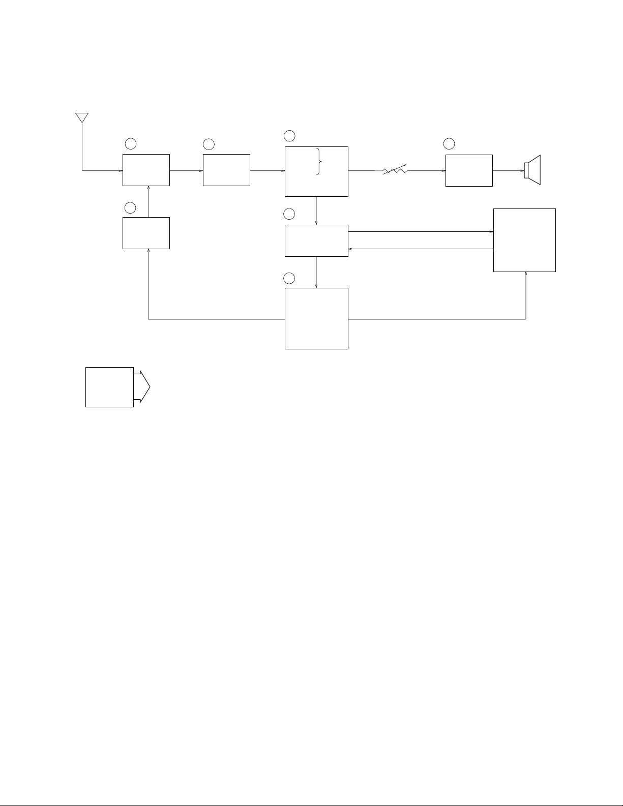
Antenna
1 TU200 2 Q200 3 IC200
7
Tuning
Voltage
Generator
VR600
Volume
Control
4 IC600 Speaker
IC300
IC700
LCD
Chroma
Circuit
Display
Control
Auto-Tuning
Control
5
6
VCC2 (4.5 ± 0.02 V)
VCC7 (25.9 ~ 31.3 V)
VCC6 (10.8 ~ 12.0 V)
VEE1 (–8.5 ~ –7.5 V)
VEE2 (–19.8 ~ –17.2 V)
IC270
Power
Supply
Audio
Amp.
IF Amp.Tuner
Video
Sound Det.
FM
AFT Circuit
AGC Circuit
Det
1— Color tuner: TU200 TEPU5-02
Selects a desired radio wave and changes it to the video IF signal.
2— Video IF amp.: Q200 2SC4238
Amplifies the video IF signal output from tuner TU200 by 10 times (20 dB).
3— Video det./Sound det./FM det./AFT/AGC: IC200 M51348FP
Eliminatesthe carrier waveinthe video IFsignal,and picks upthevideo signal andthesound IF signal.
Also, the sound signal is picked up from the sound IF signal by FM detection.
4— Audio amp.: IC600 NJM2070M
Sound amplification.
5— Chroma circuit: IC300 IR3P90Y
Generates the tricolor (red, green, and blue) from the video signal.
6— Display control/Auto-tuning control: IC700 MSM6770GS
Controls the display.
7— Tuning voltage generator: IC270 BA10358F
Generates the tuning voltage with the tuning pulse output from 6.
BLOCK DIAGRAM

— 4 —
Vcc1-1
CP100
R108
270 K
R110
270
Q110 2SD1819A-R
Q111
2SD1119-R
C137
R107
D100
MA142WK 33 K B6800 p
C140
470 p R115
100
6.3 V 220C100
D110
MA3051-L
2.2
BH102K
TM100
Q101
2SD1819A-R
2.2KR113
R105
3.3 K
VR100
2 K
C105
GND
C145
B1500 p
CP101
1
2
9
6
3
4
5
6
7
8
T100
LC12U-35 D158 MA143A R160
68
(D: 180)
C146 220 p
D156 MA142WK
D154 MA142WK
D150
MA142WK
D152
MA142WK
L101
100 u
L102
330 u
CP110
CP111
CP113
CP114
CP115
C110 25 V 10
C114 6.3 V 220
C116 6.3 V 220
C120 35 V 22
R150 33 K
Vcc2-2
Vcc7 (29.5 V)
Vcc6 (11 V)
Vcc2-1 (4.5 V)
VEE1 (-7.5 V)
VEE2 (-18 V)
GND
(3.9 V)
C112 16 V 47
C118 16 V 22
C150 OPEN
CIRCUIT DESCRIPTION
POWER SUPPLY
Figure 1
Name Voltage Function
VCC2-1 4.50 ±0.02 V Main voltage
VCC7 25.9 ~ 31.3 V Tuning voltage
VCC6 10.8 ~ 12.0 V Display voltage
VEE1 –8.5 ~ –7.5 V Display voltage
VEE2 –19.8 ~ –17.2 V Display voltage
Table 1
The power supply consists of a DC-DC converter and the associated circuit and supplies the voltages as shown
in Table 1.
— 5 —
VR100
T201T200
ADJUSTMENT
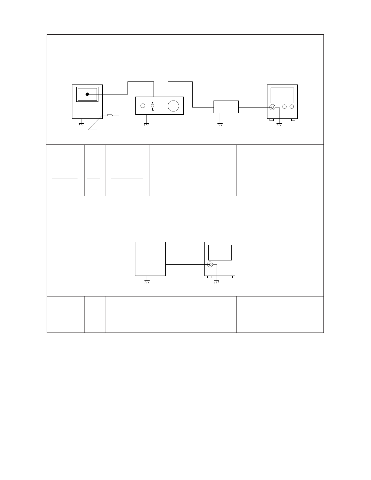
LINEAR PCB
Items to Be Adjusted
Item Measuring Instrument
VCC2-1 voltage setting Voltmeter
Video detection coil adjustment TV signal generator, pattern generator, oscilloscope,
low-pass filter
AFT coil adjustment Sweep generator, oscilloscope, voltmeter
Contrast adjustment TV signal generator, pattern generator, oscilloscope
Tint adjustment TV signal generator, pattern generator, oscilloscope
AGC adjustment TV signal generator, pattern generator, IF levelmeter
Vcom adjustment Photo diode, photo sensor amp., bandpass filter, oscilloscope
Free-Running frequency adjustment
Frequency counter
Adjustment and Test Point Locations
Top View

— 6 —
TP2(CP221)
TP7(CP207)
VR200
TP3(CP245)
TP4(CP240)
TP8(VCOM)
TP1(CP113)
VR740
VR303
TP5(CP323)
TP6(CP311)
VR300
T300
IF Pad
VCC2-1 Voltage Setting
Input Input Input Output Output
Connection Point Signal Connection Point
Adjust Result
Adjust to obtain a 4.50 ±0.02 V
reading on the voltmeter.
Voltmeter
VR100 TP1
TP1
16-169
Equipment Connection / Adjustment Procedure
Bottom View
Output
Voltmeter
EV-500
set

— 7 —
Video Detection Coil Adjustment
TP2 VR300 TP5
Pattern
generator
Signal
generator
Oscilloscope
* Desolder the IF pad to open.
Contrast Adjustment
TP2 T201 TP4
Adjust to obtain a 1.4 ±0.2 V
reading on the voltmeter.
Confirm that the marker is at
the middle of the S-curve on
the oscilloscope.
* Desolder the IF pad to open.
AFT Coil Adjustment
Pattern
generator
Signal
generator
TP2 T200 TP3
Input Input Input Output Output
Connection Point Signal Connection Point
Adjust Result
* Desolder the IF pad to open.
Voltmeter
Oscilloscope
Sweep
generator
Pattern
generator Signal
generator
Input
TP2
CP312 (KILLER)
Oscilloscope
Vcc2-3
EV-500
set 10 kohm
Adjust so
that the step
form wave
becomes 2.2
±0.1 Vp-p.
Adjust to obtain the minimum
DC level.
Low-pass filter
Oscilloscope
2.2±0.1 V
P.P
Input
TP2
EV-500
set
Output
TP3
Low-pass
filter
Pattern
generator Signal
generator Oscilloscope
Sweep
generator EV-500
set
Input
TP2 Output
TP4
Voltmeter
Oscilloscope
Color bar
38.9 MHz
(EV-200C,I,N)
39.5 MHz
(EV-200D)
45 ±3 dBµ
38.9 ±5 MHz
(sweep) marker:
38.9 MHz (EV-200C,I,N)
39.5 ±5 MHz
(sweep) marker:
39.5 MHz (EV-200D)
70 ±3 dBµ
Output
TP5(VC)
Color bar
38.9 MHz
(EV-200C,I,N)
39.5 MHz
(EV-200D)
70 ±3 dBµ

— 8 —
* Desolder the IF pad to open.
BCC Adjustment
Signal
generator
Pattern
generator EV-500
set Oscilloscope
Input
TP2 Output
TP5(VC)
Input Input Input Output Output
Connection Point Signal Connection Point
Adjust Result
Pattern
generator
Signal
generator TP2 T300 Oscilloscope TP5
Adjust T300 so that the
difference
between pulses
A and B is less
than 0.2 V.
Pulse BPulse A
AGC Adjustment
Signal
generator
Pattern
generator EV-500
set IF levelmeter
Input
TP7 Output
TP2
* Short the IF pad.
Pattern
generator
TV signal
generator TP7 VR200 IF levelmeter TP2
Color bar
65 ±5 dBµAdjust to obtain a 84 ±2 dBµ
reading on the IF levelmeter.
Vcom Adjustment
EV-500
set Oscilloscope
Output
TP8
Color bar
38.9 MHz
(EV-200C,I,N)
39.5 MHz
(EV-200D)
70 ±3 dBµ
5.0 ± 0.5 V
-0.5 ± 0.25 V
VR303 Oscilloscope TP8
Adjust VR303 so that the
high level of the square wave
is at -0.3
±0.25 V.
— 9 —
Vcom Adjustment
* Place a photo diode on the middle of the display plate.
EV-500
set Photo
diode
ON
OFF
H
M
L
AV-C1
Audio/Video jack
Bandpass
filter
Oscilloscope
Photo sensor amp.
Input Input Input Output Output
Connection Point Signal Connection Point
Adjust Result
Adjust to obtain the minimum
ripple.
VR303
Photo sensor
amp.
Bandpass filter
Oscilloscope
Free-Running Frequency Adjustment
Frequency
counter
VR740 TP6
Output
TP6
Frequency
counter
EV-500
set
Adjust to obtain a reading of
15.625 ±0.1 kHz.
This manual suits for next models
7
Table of contents
Other Casio Portable TV manuals

Casio
Casio EV-2500C Troubleshooting guide

Casio
Casio FV-600P Troubleshooting guide

Casio
Casio TV-770B Troubleshooting guide

Casio
Casio EV-510C Troubleshooting guide

Casio
Casio TV-1450C User manual

Casio
Casio SY-20B User manual

Casio
Casio TV-M430S Troubleshooting guide

Casio
Casio TV-350C Troubleshooting guide

Casio
Casio TV-880C User manual

Casio
Casio TV-600D User manual


