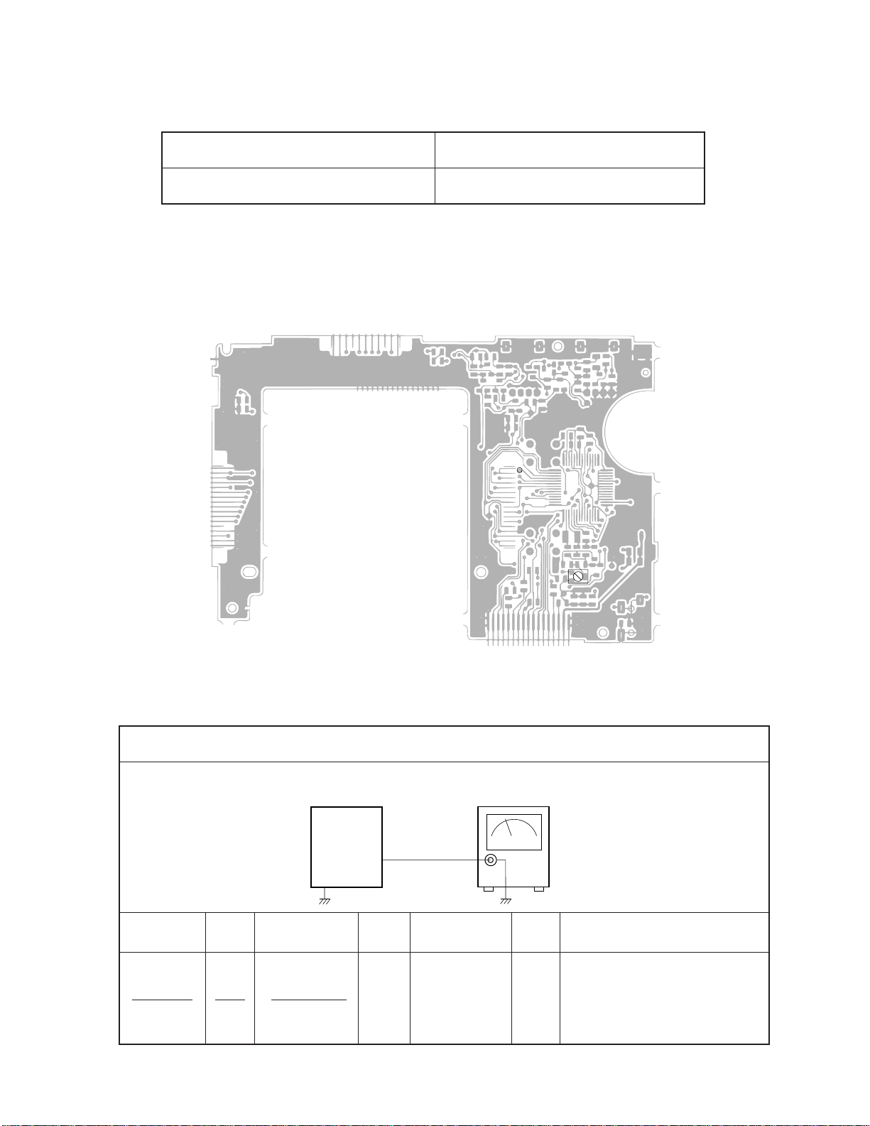
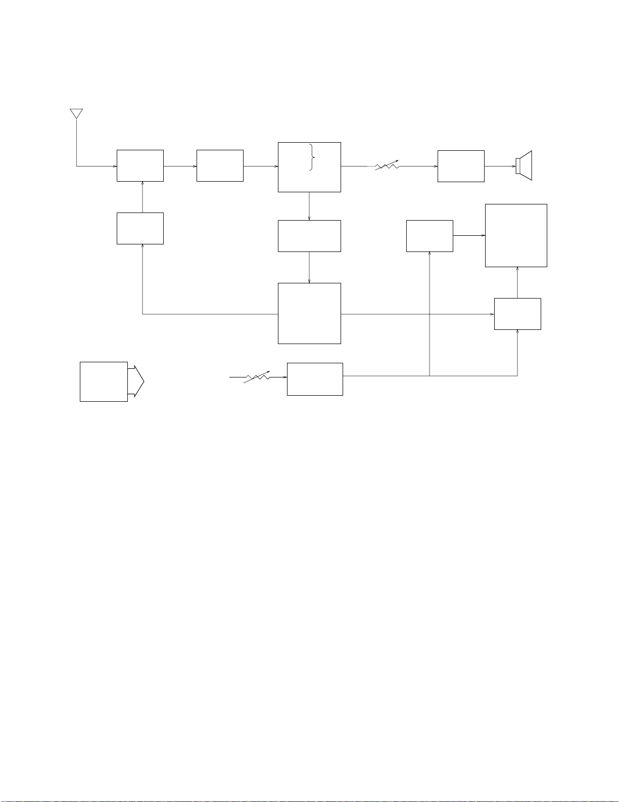
Casio TV-600G Troubleshooting guide

R
(with price)
Page
Specifications.............................................................................................1
Block Diagram ...........................................................................................2
Circuit Description......................................................................................3
Adjustment
Linear PCB..........................................................................................5
A/D PCB..............................................................................................9
Troubleshooting.......................................................................................10
Printed Circuit Boards..............................................................................11
Wiring Diagram........................................................................................15
Exploded View / Disassembly..................................................................16
Electrical Parts List ..................................................................................17
Mechanical Parts List...............................................................................23
IC and Transistor Lead Identification .......................................................24
Schematic Diagrams and Waveforms .....................................................26
POCKET TELEVISION
MARCH 1995
TV-600G/H(KX-507G/H)
INDEX

SPECIFICATIONS
— 1 —
Item Specification
1. Reception channels VHF : 2 ~ 13 ch UHF : 14 ~ 69 ch
2. Power voltage DC 6.0 V
3. Power consumption Approx. 3.4 W
4. Current consumption Approx. 566 mA
5. Battery life (with alkaline batteries) Approx 3.0 hours
Batteries : 4 AA size batteries
6. Power supply Car adaptor : CA-K65
AC adaptor : ADK-65, 64
Earphone jack : 3.5ø mini
7. Connection terminals External power jack : 6.0V DC IN
External antenna jack : 3.5ø mini
Audio / Video jack : 3.5ø
8. Screen size 2.2 inches
9. No. of Picture element 39,600 (110 ×360) dots
10. Dimensions 81 (W) ×32 (D) ×131 (H) mm
3 1/5" (W) ×1 1/4" (D) ×5 1/6" (H)
11. Weight 220 g excepting batteries
7.8 oz excepting batteries
12. Standard accessories Test batteries (R6 × 4)
AC adaptor : AD-K65, 64
13. Options Car adaptor : CA-K65
RF connector : CF-13
Antenna matching device : AS-35S
14. Body color Black

— 2 —
Antenna
1TU200 2Q200 3IC200
7
Tuning
Voltage
Generator
VR600
Volume
Control
4IC600 Speaker
IC300
IC700
Common
Driver LCD
Segment
Driver
Chroma
Circuit
Osc.
Display
Control
A-D Converter
Auto-Tuning
Control
5
6
8Q800~Q802, Q804~Q806
VR800 Display
Voltage
Generator
Brightness
Control
VCC2 (3.95±0.02 V)
VCC6 (30.5~39.0 V)
VCC7 (53.5~72.5 V)
VEE1 (–6.3~–7.9 V)
IC500
Power
Supply
Audio
Amp.
IF Amp.Tuner
Video
Sound Det.
FM
AFT Circuit
AGC Circuit
Det
1— Color Tuner: TU200 TEPU5-02
Selects a desired radio wave and changes it to the video IF signal.
2— Video IF Amp.: Q200 2SC4238
Amplifies the video IF signal output from the tuner TU by 10 times (20 dB).
3— Video Det./Sound Det./FM Det./AFT/AGC: IC200 M51348FP
Eliminatesthe carrier wavein the video IF signal,and picks upthe video signal and thesound IF signal.
Also, the sound signal is picked up from the sound IF signal by FM detection.
4— Audio Amp.: IC600 NJM2070M
Sound amplification.
5— Chroma Circuit: IC300 M52042FP
Generates the tricolor (red, green, and blue) from the video signal.
6— Osc./A-D Converter/Display Control/ Auto-Tuning Control : IC700 MSM6625-02 GSK-640F
Converts the color signal into a digital signal.
Also, generates the clock pulse for the display and controls the display.
7— Tuning Voltage Generator: IC500 MSC1169MS-K
Generates the tuning voltage with the tuning pulse (TU) output from 6.
8— Display Voltage Generator: Q800~Q802, Q804~Q806, 2SD601A-R x 4, 2SB709A-R, 2SD1149-S
Generates the display voltages V0 ~ V4 with VEE1 and VCC7 outputs from the power supply.
BLOCK DIAGRAM

— 3 —
BT
BS
VCC6
TU
H/L
BU
VREF
GND
16
15
14
13
12
11
10
9
1
2
3
4
5
6
7
8
Vcc
BS
BT
IN
OUT
TU
H/L
U/V
VREF
U1
U2
VL1
VL2
VH1
VH2
GND
R500R501R502
IC500 MSC1169MS-K
Function
CIRCUIT DESCRIPTION
TUNING VOLTAGE GENERATOR
Table 1
Figure 2
Figure 1
This circuit generates the DC tuning voltage BT for selecting a channel with a TU pulse being output from
IC700.
IC500 has 3 circuits for converting pulses to voltages; it selects one of VHF-L, VHF-H, or UHF, and
causes the tuning voltage to be output from the OUT terminal (pin 12). Figure 2 and Table 1 show the
conditions for selection.
IC500
TU OUT(BT)
U/V H/L
VHF
-H
UHF
VHF
-L
11
910
12
U/V
L
L
H
H
H/L
L
H
L
H
Inputs
VHF-L receiving
VHF-H receiving
UHF receiving
UHF receiving

— 4 —
Vref
7
6
5
32
D152
D155
D150
VCC7
VCC2
VEE1
R111
T100
R117
C105
C100
Q111
C140
R115
C145
1
9
Q101
Q100
R101
VR100
D100
C115
C114
L102
R133
VCC2-3
VCC2-2
L101
C113
C110
C112
C135
R102
CP100
VCC1-1
CP109
CP108
CP110
GND
CP104
4VCC6
CP107
D152
POWER SUPPLY
Figure 3
Name Voltage Function
VCC2 3.95 ±0.02 V Main voltage
VCC6 30.5 ~ 39.0 V Tuning voltage
VCC7 53.5 ~ 72.5 V Tuning voltage/Display voltage
VEE1 –6.3 ~ –7.9 V Display voltage
The power supply consists of a DC-DC converter and causes the voltages to be output as shown in Table 2.
Table 2

— 5 —
ADJUSTMENT
LINEAR PCB
Items To Be Adjusted
Item Measuring Instrument
VCC2 voltage setting Voltmeter
Video detection coil adjustment TV signal generator, pattern generator, oscilloscope,
low-pass filter
AFT coil adjustment Sweep generator, oscilloscope, voltmeter
Contrast adjustment TV signal generator, pattern generator, oscilloscope
AGC adjustment TV signal generator, pattern generator, IF levelmeter
Adjustment And Test Point Locations
Top View
T201
T200

— 6 —
Equipment Connection / Adjustment Procedure
Bottom View
TP5
VR300
TP7
TP1
VR100
VR200
TP3
TP4
TP2
PadIF
VCC2 Voltage Setting
Input Input Input Output Output
Connection Point Signal Connection Point
Adjust Result
Adjust for 3.95 ±0.02 V
reading on voltmeter.
Voltmeter
VR100
Set
Output
Voltmeter
TP1
TP1
TV-600

— 7 —
Video Detection Coil Adjustment
TP2 VR300 TP5
Pattern
generator
Signal
generator
Color bar
45.75 MHz
70 ±3 dBµOscilloscope Adjust step form wave to read
0.8 ±0.05 Vp-p.
Signal
generator
Pattern
generator Set Oscilloscope
Input Output
TP5
TP2
* Desolder the IF pad to open.
Contrast Adjustment
TP2 T201 TP4
Adjust for 2.0 ±0.2 V reading
on voltmeter.
Confirm that the marker is at
the middle of S-curve on oscil-
loscope.
Sweep
generator Set Oscilloscope Voltmeter
Output
Input
* Desolder the IF pad to open.
TP2 TP4
AFT Coil Adjustment
Pattern
generator
Signal
generator
TP2 T200 TP3
Low-pass filter
Oscilloscope
Color bar
45.75 MHz
40 ±3 dBµAdjust for DC level at mini-
Input Input Input Output Output
Connection Point Signal Connection Point
Adjust Result
* Desolder the IF pad to open.
Signal
generator
Pattern
generator Set Low-pass
filter
Oscilloscope
Input Output
TP3
TP2
Voltmeter
Oscilloscope
Sweep
generator
45.75±5 MHz
(Sweep) Marker:
45.75 MHz
70 ±3 dBµ
TV-600
TV-600
TV-600

— 8 —
AGC Adjustment
Signal
generator
Pattern
generator Set
Input Output
IF levelmeter
TP2
TP7
TV-600
Pattern
generator
TV signal
generator
TP7 VR200 IF levelmeter TP2
Input Input Input Output Output
Connection Point Signal Connection Point
Color bar
65 ±5 dBµAdjust for 84 ±2 dBµ
reading on the IF levelmeter
* Short the IF pads.
Adjust Result

— 9 —
A/D PCB
Item to Be Adjusted
Adjustment And Test Point Locations
Item Measuring Instrument
Clock adjustment Voltmeter
TOP VIEW
TP6
VR700
Clock Adjustment
Voltmeter
VR700 TP6
Equipment Connection / Procedure
Adjust for 2.05 ±0.05 V read-
ing on voltmeter.
Set
Output
Voltmeter
TP6
TV-600
Input Input Input Output Output
Connection Point Signal Connection PointAdjust Result

— 10 —
TROUBLESHOOTING
Picture OK but
no sound
Symptom Cause Solution
No power supply Defective power switch (SW100). Replace.
Defective DC-DC converter (T100). Replace.
Defective tuner (TU200). Replace.
Defective Q200. Replace.
Defective IC200. Replace.
Defective IC300. Replace.
Defective IC500. Replace.
Defective IC700. Replace.
Defective F201 (ceramic discriminator). Replace.
Defective IC200. Replace.
Defective IC700. Replace.
Defective phone jack (JK600). Replace.
Defective tuner (TU200). Replace.
Defective IC500. Replace.
Defective power switch (SW100). Replace.
No reception of
VHF or UHF
No picture and
no sound

— 11 —
PRINTED CIRCUIT BOARDS
TOP VIEWS
Linear
BL
T950
C925
C927
L950
Q950
Q951 R950 507BL
1
DB –DB –DB –
CN700
+
+
C110
C105
T100
+
C112
C100
+
+
C115
L101
C114
+
+
C113
T201T200
C210
R223
L102
+
R222
+
F202
C208
FU100
D180
JK100
DB +DB +
C244
+
C207
F201
SW100
C305 F200
L202
+
C309
+
H300
C340
C345
R310
C348
R322
R326
R346
R336
R335
C291
R247
C290
R133
TU200
C202
+
JK200

— 12 —
VR100
R500
C550 R115
R212
R210 C262
C237
R204 C240
L200C335
R307 R306
C146
R246 C249
C185
C259
R236
C351
R330
C330
Q300
VR300
VR301
VR200
IC300 IC200
IC500
D155
D152
D154
D100 D150
Q101
Q100
Q200
HP200
CP327 CP326
CP325
CP207 CP210
CP209
R224
CP208
CP204
CP203
C234
CP541
R545
C545
C235
R541
R550
CP500
R502
R501
C135R101
R117
C140
R111
CP110
Q111
CP542
CP322
CP320
CP235
CP236
CP108
CP104
CP100
CP107
CP206
CP221
R201
C233
R207
R202
C236
R203
R205
R305
CP340
CP330
R208
R209 C245
C263C261 C264
CP240
R230
R229
C257
CP211
CP245
R331
C350
R325
C246
CP224
CP590
CP109
C145
BOTTOM VIEWS
Linear
BL
HP903 HP902
FU900
FU901
HP906
HP905
HP950
HP900
HP901

— 13 —
IC703
C770
C775
IC702
C835
R808
R814
R810
R800
C830
R827
R740
R727
R815
Q802 Q801
C836
R816
Q800
R809
D800
R833
Q805
D805
R830
Q806 Q804
R825
R824
R845
C841
D803
C840 R820
R726
R725
SW700
UP
SW701
DOWN
IC700
R700
R803
R704
R611
C642
C630
C755
C756
C760 R730
D705
L705
VR700
D707
17
HP700
R710
R706
R707
R610
R733C758
R606
R607
R645
R738
IC701
TOP VIEW
A/D

— 14 —
BOTTOM VIEW
A/D
STB
D4
D5
V4
CDB2
VC
CNB2
V0
CFB2 VCC2-8
V3
D6
D3 D2 D1
SNB
CK2
CK1
PD
GND2
VR600
VR800
GND1
R615
C740C741
D700 D701
C761
C734
IC600
JK600
C742
C750
C751
R719
C635
R641
BL+
BL-
SP-
SP+ C765
C603
C606
C806
C808
C800

— 15 —
WIRING DIAGRAM
TOP VIEWS
1
17
1
17
A/D PCB
Linear PCB

— 16 —
EXPLODED VIEW / DISASSEMBLY
18
16
19
17
14
15
20
11
12
9
7
8
10
13
7
8-5
12-1
12-2
15-1
15-2
15-3
8-1 8-2 8-3
8-4
8-2
6-3
1
3
4
5
6
2
7
7
6-5
6-6
6-7
6-8
6-9 6-10
2-1
2-2
6-1 6-2
6-4

ELECTRICAL PARTS LIST
Linear PCB No. 1 FOB Japan
N Item Code No. Parts Name Specification Q'ty M N.R.Yen R
G H Unit Price
Capacitors
C100 2805 2180 Electrolytic capacitor (V) 10RE2-220 1 1 20 26 C
C105 2801 7630 Electrolytic capacitor (V) 6.3RC2-47MS-G12 1 1 20 13 C
C110 2805 2430 Electrolytic capacitor (V) 16RC2-10-G11 1 1 20 19 C
N C112 2806 9434 Electrolytic capacitor 6.3RC2-220MS-G11 1 1 20 15 C
C113 2828 5552 Electrolytic capacitor 6.3RV2-100-T 1 1 20 24 C
C114 2807 6938 Electrolytic capacitor 50RV2-4R7-T 1 1 20 22 C
C115 2805 9582 Electrolytic capacitor (V) 100RC2-1 1 1 20 14 C
C135 2897 0112 Chip capacitor GR40W5R562K50PT 1 1 20 12 C
C140 2897 0259 Chip capacitor GR40W5R332K50PT 1 1 20 7 C
C145 2892 0016 Chip capacitor GR40W5R102K50PT 1 1 20 11 C
C146 2897 1617 Chip capacitor GR40CH221J200PT 1 1 20 15 C
C185 2892 0040 Chip capacitor GR40Y5V104Z25PT 1 1 20 14 C
C202 2800 9182 Electrolytic capacitor 6.3RC2-47MS 1 1 20 15 C
C207 2807 6553 Electrolytic capacitor 6.3RV2-47-T 1 1 20 22 C
C208 2804 9714 Electrolytic capacitor 6.3RC347-G11 1 1 20 14 C
C210 2804 9641 Electrolytic capacitor (V) 16RC310-G11 1 1 20 25 C
C233 2892 0059 Chip capacitor GR40Y5V103Z50PT 1 1 20 9 C
C234 2892 0059 Chip capacitor GR40Y5V103Z50PT 1 1 20 9 C
C235 2897 0924 Chip capacitor GR42-6W5R823K50PT 1 1 20 18 C
C236 2892 0059 Chip capacitor GR40Y5V103Z50PT 1 1 20 9 C
C237 2892 0059 Chip capacitor GR40Y5V103Z50PT 1 1 20 9 C
C240 2892 0059 Chip capacitor GR40Y5V103Z50PT 1 1 20 9 C
C244 2895 1099 Tantalum capacitor ECST1CY225R 1 1 20 21 C
C245 2892 0229 Chip capacitor GR40W5R103K25PT 1 1 20 12 C
C246 2892 0059 Chip capacitor GR40Y5V103Z50PT 1 1 20 9 C
C249 2892 0844 Chip capacitor GR42-6Y5V474Z16PT 1 1 20 27 C
C257 2892 0407 Chip capacitor GR40CH270J50PT 1 1 20 10 C
C259 2897 0539 Chip capacitor GR40W5R223K50PT 1 1 20 12 C
C261 2892 0890 Chip capacitor GR40PH560J50PT 1 1 20 13 C
C262 2897 2058 Chip capacitor GR40PH470J50PT 1 1 20 5 C
C263 2892 0890 Chip capacitor GR40PH560J50PT 1 1 20 13 C
C264 2897 0133 Chip capacitor GR40CH0R5C50PT 1 1 20 7 C
C290 2845 5537 Chip capacitor UMK212CH161J-T 1 1 20 4 C
C291 2897 0455 Chip capacitor GR40CH360J50PT 1 1 20 3 C
C305 2804 9064 Electrolytic capacitor (V) 16RC2-10 1 1 20 9 C
N C309 2800 9182 Electrolytic capacitor 6.3RC2-47MS 1 1 20 15 C
C330 2897 1827 Chip capacitor EMK316B474K-T 1 1 20 22 C
C335 2845 1344 Chip capacitor GR40W5R471K50PT 1 1 20 4 C
C340 2892 0229 Chip capacitor GR40W5R103K25PT 1 1 20 12 C
C345 2897 0112 Chip capacitor GR40W5R562K50PT 1 1 20 12 C
C346 2897 0973 Chip capacitor GR40W5R683K25PT 1 1 20 16 C
C347 2897 0973 Chip capacitor GR40W5R683K25PT 1 1 20 16 C
C350 2892 0415 Chip capacitor GR40CH181J50PT 1 1 20 12 C
C351 2892 0458 Chip capacitor GR40CH220J50PT 1 1 20 6 C
C545 2897 0693 Chip capacitor GR40W5R333K25PT 1 1 20 12 C
C550 2897 0021 Chip capacitor GR40Y5V683Z50PT 1 1 20 27 C
Connector
CN700 3501 8631 Connector 9603S-17C 1 1 20 27 C
Diodes
D100 2390 1176 Chip diode MA152WK-(TX) 1 1 20 8 C
D150 2390 1176 Chip diode MA152WK-(TX) 1 1 20 8 C
Notes: N – New parts
M – Minimum order/supply quantity
R – Rank — 17 —

Linear PCB No. 2 FOB Japan
N Item Code No. Parts Name Specification Q'ty M N.R.Yen R
G H Unit Price
D152 2390 1176 Chip diode MA152WK-(TX) 1 1 20 8 C
D154 2390 1176 Chip diode MA152WK-(TX) 1 1 20 8 C
D155 2390 1302 Chip diode MA153A-(TX) 1 1 20 21 C
D180 2390 1190 Chip diode ERA15-01Y 1 1 20 9 C
Filters
F200 3025 0182 SAW filter SAF45MA60Z 1 1 1 140 C
F201 3025 0714 SIF filter SFSL4.5MDB12 1 1 10 33 C
F202 3851 1057 Ceramic discriminator CDSL4.5MC30C12 1 1 10 42 C
Fuse
FU100 3632 0469 Fuse PI-251001(F10) 1 1 10 52 C
Oscillators
N H300 2590 1477 Crystal oscillator HC-49U-G13 1 0 5 93 C
N H300 2590 1505 Crystal oscillator HC-49U-H13 0 1 5 93 C
ICs
IC200 2114 1827 Linear IC M51348FP-T1 1 1 1 190 B
IC300 2114 3311 Linear IC M52045FP-T1 1 1 1 300 B
IC500 2114 0182 Linear IC MSC1169MS-K-620 1 1 1 140 B
Jacks
JK100 3501 8281 Jack HEC0811-010010 1 1 10 43 C
JK200 3501 5439 Jack HSJ1456-01-210 1 1 20 27 C
Inductors
L101 3013 1379 Chip inductor LEM4532-101K-TP 1 1 20 24 C
L102 3013 1379 Chip inductor LEM4532-101K-TP 1 1 20 24 C
L200 3013 1393 Chip inductor LK2125-R82K-TP 1 1 20 26 C
L202 3013 1659 Chip inductor PL0203S-8R2J-7 1 1 20 16 C
Transistors
Q100 2210 8026 Chip transistor 2SB709A-R(TX) 1 1 20 23 C
Q101 2230 7011 Chip transistor 2SD601A-R(TX) 1 1 20 22 C
Q111 2253 0308 Chip transistor 2SD1119-R(TX) 1 1 10 37 C
Q200 2252 0707 Chip transistor 2SC4238-(TX) 1 1 20 17 C
Q300 2210 8026 Chip transistor 2SB709A-R(TX) 1 1 20 23 C
Resistors
R101 2791 1595 Chip resistor ERJ-6GEYJ153V 1 1 20 4 C
R111 2791 0815 Chip resistor ERJ-6GEYJ102V 1 1 20 5 C
R115 2791 2117 Chip resistor ERJ-6GEYJ820V 1 1 20 4 C
R117 2791 0696 Chip resistor ERJ-6GEYJ470V 1 1 20 4 C
R133 2791 1617 Chip resistor ERJ-6GEYJ100V 1 1 20 3 C
R201 2791 2117 Chip resistor ERJ-6GEYJ820V 1 1 20 4 C
R202 2791 0305 Chip resistor ERJ-6GEYJ472V 1 1 20 3 C
R203 2791 0720 Chip resistor ERJ-6GEYJ222V 1 1 20 3 C
R204 2791 0704 Chip resistor ERJ-6GEYJ561V 1 1 20 4 C
R205 2791 0688 Chip resistor ERJ-6GEYJ220V 1 1 20 3 C
R207 2791 1161 Chip resistor ERJ-6GEYJ151V 1 1 20 5 C
R208 2791 0734 Chip resistor ERJ-6GEYJ272V 1 1 20 3 C
R209 2791 0313 Chip resistor ERJ-6GEYJ103V 1 1 20 5 C
R210 2791 0305 Chip resistor ERJ-6GEYJ472V 1 1 20 3 C
R212 2791 0720 Chip resistor ERJ-6GEYJ222V 1 1 20 3 C
R222 2791 0696 Chip resistor ERJ-6GEYJ470V 1 1 20 4 C
R223 2791 0615 Chip resistor ERJ-6GEYJ154V 1 1 20 5 C
R224 2797 1127 Chip resistor ERJ-6GEYK475V 1 1 20 3 C
R229 2791 1170 Chip resistor ERJ-6GEYJ182V 1 1 20 3 C
R230 2791 0704 Chip resistor ERJ-6GEYJ561V 1 1 20 4 C
R236 2791 2044 Chip resistor ERJ-6GEYJ124V 1 1 20 3 C
R246 2791 1420 Chip resistor ERJ-6GEYJ331V 1 1 20 6 C
Notes: N – New parts
M – Minimum order/supply quantity
R – Rank — 18 —

Linear PCB No. 3 FOB Japan
N Item Code No. Parts Name Specification Q'ty M N.R.Yen R
G H Unit Price
R247 2791 0720 Chip resistor ERJ-6GEYJ222V 1 1 20 3 C
R305 2791 0815 Chip resistor ERJ-6GEYJ102V 1 1 20 5 C
R306 2791 1390 Chip resistor ERJ-6GEYJ473V 1 1 20 5 C
R307 2791 0712 Chip resistor ERJ-6GEYJ152V 1 1 20 4 C
R310 2791 1579 Chip resistor ERJ-6GEYJ474V 1 1 20 4 C
R322 2791 0607 Chip resistor ERJ-6GEYJ333V 1 1 20 4 C
R325 2791 1684 Chip resistor ERJ-6GEYJ183V 1 1 20 3 C
R326 2797 1015 Chip resistor ERJ-6GEYK225V 1 1 20 3 C
R330 2795 3829 Chip resistor ERJ-6GEYJ302V 1 1 20 3 C
R331 2797 1589 Chip resistor ERJ-6GEYJ511V 1 1 20 3 C
R335 2791 0750 Chip resistor ERJ-6GEYJ223V 1 1 20 6 C
R336 2791 0769 Chip resistor ERJ-6GEYJ563V 1 1 20 3 C
R500 2791 0777 Chip resistor ERJ-6GEYJ104V 1 1 20 5 C
R501 2791 0769 Chip resistor ERJ-6GEYJ563V 1 1 20 3 C
R502 2791 1919 Chip resistor ERJ-6GEYJ274V 1 1 20 3 C
R541 2791 0750 Chip resistor ERJ-6GEYJ223V 1 1 20 6 C
R545 2791 1579 Chip resistor ERJ-6GEYJ474V 1 1 20 4 C
R550 2791 0815 Chip resistor ERJ-6GEYJ102V 1 1 20 5 C
Switch
SW100 3412 0798 Slide switch ESD-11H231 1 1 10 47 C
Coils and Converter
T100 3065 0441 DC-DC converter LC12U-29 1 1 5 73 C
T200 3841 0721 Coil 5KVC-07A 1 1 10 48 C
T201 3841 0728 Coil 5KAC-02A 1 1 10 49 C
Tuner
TU200 1013 5511 Tuner TEPU5-02 1 1 1 760 C
Variable resistors
VR100 2775 1316 Semi-fixed resistor EVM-1SSW50B53 1 1 20 27 C
VR200 2775 1211 Semi-fixed resistor EVM-1SSW50B54 1 1 20 27 C
VR300 2775 1211 Semi-fixed resistor EVM-1SSW50B54 1 1 20 27 C
VR301 2775 1211 Semi-fixed resistor EVM-1SSW50B54 1 1 20 27 C
Notes: N – New parts
M – Minimum order/supply quantity
R – Rank — 19 —
This manual suits for next models
3
Table of contents
Other Casio Portable TV manuals

Casio
Casio FV-600P Troubleshooting guide

Casio
Casio TV-1450C User manual

Casio
Casio EV-510C Troubleshooting guide

Casio
Casio EV-600B Troubleshooting guide

Casio
Casio TV-880C User manual

Casio
Casio EV-500C Troubleshooting guide

Casio
Casio TV-880B Troubleshooting guide

Casio
Casio TV-600B Troubleshooting guide

Casio
Casio EV-2500C Troubleshooting guide

Casio
Casio SY-20B User manual