Seavice
MANUAL
&
PARTS
LIST
soo
POCKET
TELEVISION
TV=-1450C
TV=-1450N
TV=-1450D
MAY
1991
Page
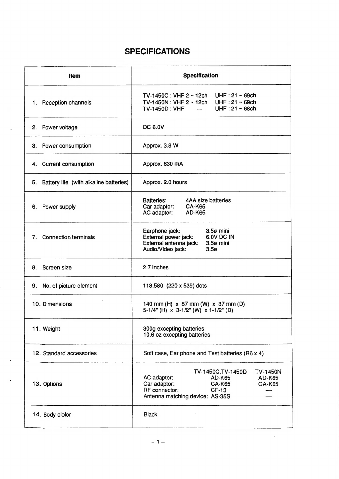
Specifications
---------------------------------2-ecn
cc
nnnn
nnn
nnnn
ncn
cn
nnn
nccn
ne
nananncnnnnncncencnns
|
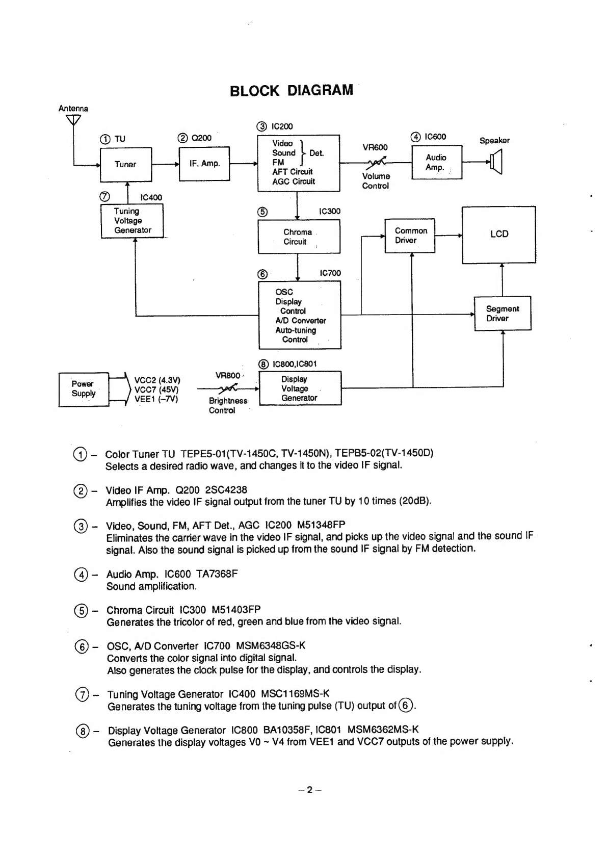
Block
DiaQram
--------------en20n=--nnnn
nnn
nnn
nn
nnn
nnn
nnn
nnn
nro
rn
rn
nnn
nnnnnannn
a
mir
2
Circuit
Operations
----------------------------nnnennnnn
nnn
nnn
nner
nen
nnnn
enon
nnn
onnonmnnnnnnnnnn
sane
3
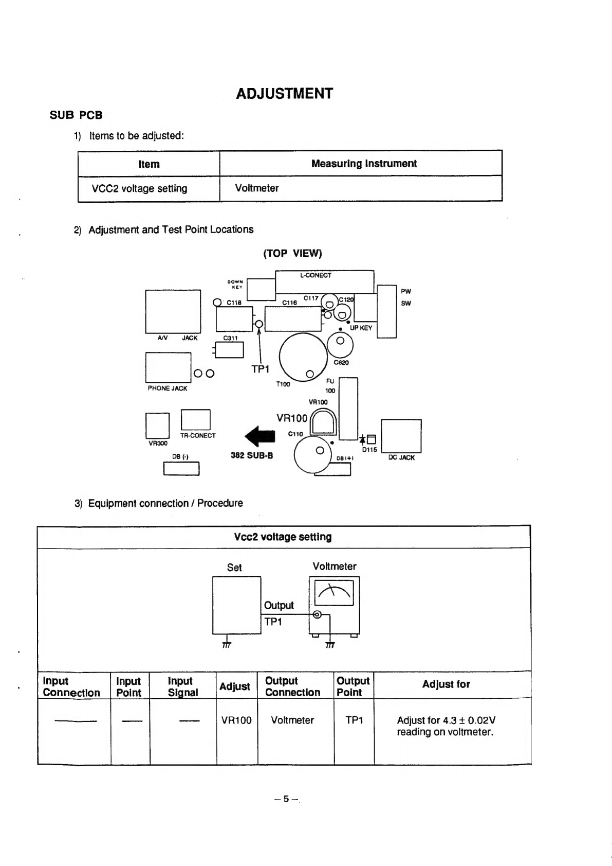
Adjustment
ee
a
Oo
a
a
5
Linear
PCB
------------------n2-n-n-nn-nennnnnnn
ence
nc
cenceneennnnncnnnnnnennnnnnencesccsenen
&
AID
PCB
~----------n--n-nnnnn
nnn
manne
nnn
n
nner
nner
nennncnnnccnncncnnncenanmmnnnnnnanans
10
Troubleshooting
------------------n-nn-n
nmr
nnn
nnn
nn
nner
nnn
nnn
nnn
nen
mn
nna
nnn
cn
emnnmnnnnns
12
Wiring
Diagram
-----------------------------n
enn
nnnn
nn
nn
nnnn
nnn
nnn
nnn
nnn
nnn
nmnnnnn
nnn
nnnn
on
17
PCB
Diagrams
----------------7--------nn
nn
nnnnn
none
nn
enn
nnnnnnnncennnnnnnnnnnnnrnnannnnnannnnenes
18
Exploded
View:/
Disassembly
==--<-s--2-+---=-sse
retire
mene
seen
eerce
ese
areeeen
eee
24
Electrical
Parts
List
-----------------------------
ns
-nn
nnn
nnn
nnn
nnn
nnn
nnn
nnn
nme
25
Mechanical
Parts
List
---------------~------------------
nnn
nn
nn
nnn
nnn
nn
nnn
ne
nnn
er
een
cnn
nnn
34
Lead
Identification
------------------------------------e---o2ncenecenccenceencees
eid
ceoeee
se
35
Schematic
Diagram
+S
37