manuals.online logo
Brands
  1. Home
  2. •
  3. Brands
  4. •
  5. Cree
  6. •
  7. Batteries Charger
  8. •
  9. Cree CRD-06600FF10N User manual

Cree CRD-06600FF10N User manual

CPWR-AN26, Rev A, 08-2018
Copyright © 2018 Cree, Inc. All rights reserved.
The information in this document is subject to change without notice.
Cree and Zero Recovery are registered trademarks, and the Cree logo and C3M are trademarks, of Cree, Inc
CRD-06600FF10N
6.6kW BI-DIRECTIONAL EV ON-BOARD CHARGER USER GUIDE
CRD-06600FF10N
6.6kW 双向电动汽车车载充电器用户指南
CRD-06600FF10N
6.6kW 双方向電気自動車車載充電器ユーザーガイド
User Guide
CPWR-AN26, Rev A
Cree Power Applications
Cree, Inc.
4600 Silicon Drive
Durham, NC 27703 USA
科税有限责任公司
4600 硅驱动器
Durham, NC 27703 USA
クリー株式会社
4600シリコンドライブ
Durham, NC 27703 USA
This document is prepared as a User’s Guide to operate Cree evaluation hardware.
All parts of this User’s Guide are provided in English, and the Cautions are provided in English, Mandarin, and
Japanese. If the end user of this board is not fluent in any of these languages, it is your responsibility to ensure that
CREE C3MTM SiC MOSFET
C3M0065100K
TO-247-4 Package
CPWR-AN26, Rev A, 08-2018
Copyright © 2018 Cree, Inc. All rights reserved.
The information in this document is subject to change without notice.
Cree and Zero Recovery are registered trademarks, and the Cree logo and C3M are trademarks, of Cree, Inc
they understand the terms and conditions described in this document, including without limitation the hazards of and
safe operating conditions for this board.
本文件中的所有内容均以英文书写,“注意”部分的内容以英文、中文和日语书写。若本板子的
终端用户不熟悉上述任何一种语言,则您应当确保该终端客户能够理解本文件中的条款与条件,
包括且不限于本板子的危险以及安全操作条件。
当書類のすべての内容は英語で書きます。「注意点」の内容は英語、中国語、また日本語で書
きます。当ボードの端末使用者は上記の言語が一つでもわからないなら、当端末使用者は当書
類の条約と条件が理解できるのを確保すべきです。そして、当ボードの危険や安全に使用する
条件を含み、また限りません。
Note: This Cree-designed evaluation hardware for Cree components is a fragile, high voltage,
high temperature power electronics system that is meant to be used as an evaluation tool in a lab
setting and to be handled and operated by highly qualified technicians or engineers. When this
hardware is not in use, it should be stored in an area that has a storage temperature ranging from
-40° Celsius to 150° Celsius and if this hardware is transported, special care should be taken
during transportation to avoid damaging the boardor its fragile components and the board should
be transported carefully in an electrostatic discharge (ESD) bag to avoid anydamage to electronic
components. The hardware does not contain any hazardous substances, is not designed to meet
any industrial, technical, or safety standards or classifications, and is not a production qualified
assembly.
本工具(一种易碎、高压、高温电力电子系统)是由科锐为其组件设计的评估硬件,旨在用作实
验室环境下的评估工具,并由够格的技术人员或工程师处理和操作。本硬件不使用时,应存储在-
40oC到150oC温度范围的区域内;如需运输本硬件,运输过程中应该特别小心,避免损坏电路板
或其易碎组件。电路板应放置在静电放电(ESD)袋中谨慎运输,避免损坏电子组件。本硬件不
含任何有害物质,其设计不符合任何工业、技术或安全标准或分类,也不是可用于生产的组件。
このクリーのコンポーネント用評価ハードウェアは壊れやすい高電圧の高温パワーエレクトロニクスシ
ステムであり、ラボ環境での評価ツールとして使用され、優秀な技術者やエンジニアによって処理され、
操作されることを意図している。ハードウェアが使用されていない場合、保管温度が-40℃から150℃の
範囲に保管してください。このハードウェアを輸送する場合は、輸送中にボードまたはその壊れやすい
コンポーネントに損傷を与えないよう特別な注意を払う必要がある。また電子部品の損傷を避けるため
にボードを静電気放電(ESD)袋に静置して慎重に輸送するべき。ハードウェアには危険物質が含まれ
ていないが、工業的、技術的、安全性の基準または分類に適合するように設計されておらず、生産適
格組立品でもない。
CPWR-AN26, Rev A, 08-2018
Copyright © 2018 Cree, Inc. All rights reserved.
The information in this document is subject to change without notice.
Cree and Zero Recovery are registered trademarks, and the Cree logo and C3M are trademarks, of Cree, Inc
CAUTION
PLEASE CAREFULLY REVIEW THE FOLLOWING PAGE, AS IT CONTAINS
IMPORTANT INFORMATION REGARDING THE HAZARDS AND SAFE OPERATING
REQUIREMENTS RELATED TO THE HANDLING AND USE OF THIS BOARD.
警告
请认真阅读以下内容,因为其中包含了处理和使用本板子有关的危险和安全操作要求方
面的重要信息。
警告
ボードの使用、危険の対応、そして安全に操作する要求などの大切な情報を含むの
で、以下の内容をよく読んでください。
CPWR-AN26, Rev A, 08-2018
Copyright © 2018 Cree, Inc. All rights reserved.
The information in this document is subject to change without notice.
Cree and Zero Recovery are registered trademarks, and the Cree logo and C3M are trademarks, of Cree, Inc
CAUTION
DO NOT TOUCH THE BOARD WHEN IT IS ENERGIZED AND ALLOW THE BULK
CAPACITORS TO COMPLETELY DISCHARGE PRIOR TO HANDLING THE BOARD.
THERE CAN BE VERY HIGH VOLTAGES PRESENT ON THIS EVALUATION BOARD
WHEN CONNECTED TO AN ELECTRICAL SOURCE, AND SOME COMPONENTS ON
THIS BOARD CAN REACH TEMPERATURES ABOVE 50˚ CELSIUS. FURTHER,
THESE CONDITIONS WILL CONTINUE FOR A SHORT TIME AFTER THE
ELECTRICAL SOURCE IS DISCONNECTED UNTIL THE BULK CAPACITORS ARE
FULLY DISCHARGED.
Please ensure that appropriate safety procedures are followed when operating this
board, as any of the following can occur if you handle or use this board without
following proper safety precautions:
● Death
● Serious injury
● Electrocution
● Electrical shock
● Electrical burns
● Severe heat burns
You must readthis document in its entirety beforeoperating this board. It isnot necessary
for you to touch the board while it is energized. All test and measurement probes or
attachments must be attached before the board is energized. You must never leave this
board unattended or handle it when energized, and you must always ensure that all bulk
capacitors have completely discharged prior to handling the board. Do not change the
devices to be tested until the board is disconnected from the electrical source and the
bulk capacitors have fully discharged.
CPWR-AN26, Rev A, 08-2018
Copyright © 2018 Cree, Inc. All rights reserved.
The information in this document is subject to change without notice.
Cree and Zero Recovery are registered trademarks, and the Cree logo and C3M are trademarks, of Cree, Inc
警告
请勿在通电情况下接触板子,在处理板子前应使大容量电容器完全释放电力。接通电源后
,该评估板上可能存在非常高的电压,板子上一些组件的温度可能超过50 摄氏度。此外
,移除电源后,上述情况可能会短暂持续,直至大容量电容器完全释放电量。
操作板子时应确保遵守正确的安全规程,否则可能会出现下列危险:
●死亡
●严重伤害
●触电
●电击
●电灼伤
●严重的热烧伤
请在操作本板子前完整阅读本文件。通电时不必接触板子。在为板子通电前必须连接所有
测试与测量探针或附件。通电时,禁止使板子处于无人看护状态,或操作板子。必须确保
在操作板子前,大容量电容器释放了所有电量。只有在切断板子电源,且大容量电容器完
全放电后,才可更换待测试器件
CPWR-AN26, Rev A, 08-2018
Copyright © 2018 Cree, Inc. All rights reserved.
The information in this document is subject to change without notice.
Cree and Zero Recovery are registered trademarks, and the Cree logo and C3M are trademarks, of Cree, Inc
警告
通電している時、ボードに接触するのは禁止です。ボードを処分する前に、大容量のコンデン
サーで電力を完全に釈放すべきです。通電してから、ボードにひどく高い電圧が存在している
可能性があります。ボードのモジュールの温度は 50 度以上になるかもしれません。また、電源
を切った後、上記の状況がしばらく持続する可能性がありますので、大容量のコンデンサーで
電力を完全に釈放するまで待ってください。
ボードを操作するとき、正確な安全ルールを守るのを確保すべきです。さもないと、以下の危
険がある可能性があります:
●死亡
●重症
●感電
●電撃
●電気の火傷
●厳しい火傷
当ボードを操作する前に、完全に当書類をよく読んでください。通電している時にボードに接
触する必要がありません。通電する前に必ずすべての試験用のプローブあるいはアクセサリー
をつないでください。通電している時に無人監視やボードを操作するのは禁止です。ボードを
操作する前に、大容量のコンデンサーで電力を完全に釈放するのを必ず確保してください。ボ
ードの電源を切った後、また大容量のコンデンサーで電力を完全に釈放した後、試験設備を取
り換えることができます。
CPWR-AN26, Rev A, 08-2018
Copyright © 2018 Cree, Inc. All rights reserved.
The information in this document is subject to change without notice.
Cree and Zero Recovery are registered trademarks, and the Cree logo and C3M are trademarks, of Cree, Inc
Table of Contents
1. Introduction ................................................................................................................... 7
2. Description ..................................................................................................................... 8
3. Electrical Performance Specifications............................................................................ 9
3.1 Applications .......................................................................................................10
3.2 Features .............................................................................................................11
4. Schematics of Power Board and Control Board ..........................................................12
5. Hardware Description of Power Board and Control Board..........................................17
6. Test Equipment ............................................................................................................19
6.1 Recommended Test Set Up (AC/DC Mode) .......................................................22
6.2 Recommended Test Set Up (DC/AC - Grid Connected Mode) ........................... 23
6.3 Recommended Test Set Up (DC/AC - OFF Grid Mode) ......................................24
6.4 Parameters which can be measured ..................................................................25
6.5 LED Indicators .....................................................................................................25
6.6 Isolated Power Supplies - Voltage and Current Settings....................................26
6.7 Potentiometer VR1 settings for various Output Votages in AC/DC Mode ........ 26
6.8 Potentiometer VR1 settings for various Grid Current values in DC/AC Mode ..26
7. Preparations for Testing The Unit for The First Time ..................................................27
7.1 Starting Procedure of The Unit in AC/DC Mode.................................................31
7.2 Stopping Procedure of The Unit in AC/DC Mode ............................................... 32
7.3 Starting Procedure of The Unit in DC/AC Grid Connected Mode ......................33
7.4 Stopping Procedure of The Unit in DC/AC Grid Connected Mode .................... 33
7.5 Starting Procedure of The Unit in DC/AC OFF Grid Mode with Resistive
Load ....................................................................................................................34
7.6 Stopping Procedure of The Unit in DC/AC OFF Grid Mode with Resistive
Load ....................................................................................................................35
8. Location of The Connectors (Power Board and Control Board) .................................. 36
9. Trip Points of Cree’s CRD-06600FF10N Reference Design Board ..............................38
10. Performance Data ......................................................................................................39
11. Typical Waveforms .................................................................................................... 42
12. Thermal Data .............................................................................................................48
13. Revision History ......................................................................................................... 49
14. Important Notes ........................................................................................................50
CPWR-AN26, Rev A, 08-2018
Copyright © 2018 Cree, Inc. All rights reserved.
The information in this document is subject to change without notice.
Cree and Zero Recovery are registered trademarks, and the Cree logo and C3M are trademarks, of Cree, Inc
Cree’s CRD-06600FF10N, 6.6KW Bi-Directional EV On-board charger (OBC) is designed to operate
from universal single-phase input and provide an output voltage in the range of 250 VDC to
450 VDC. The front-end AC/DC PFC (Power Factor Correction) stage consists of a Totem-Pole Bi-
Directional topology followed by a Bi-Directional Isolated DC/DC stage which uses a symmetric
CLLC converter. The input and output sides of the Bi-Directional Isolated DC/DC stage carry H
bridge topologies. Input is isolated from the output through a high frequency transformer. Even
though this board is designed for electric vehicle (EV) application, there is no battery charging
algorithm built in and the board must be tested on resistive load only. Output current is limited
to 20A at 250VDC output. AC/DC PFC stage runs at a fixed frequency of 67 kHz and DC/DC CLLC
stage runs at fixed frequency close to 200 kHz. The output voltage is regulated by varying DC link
voltage, which is an open loop control. Output voltage can be set by a potentiometer provided
on the control board. A block diagram of Cree’s CRD-06600FF10N, 6.6KW Bi-Directional EV On-
board charger is shown in Figure 1.
Figure 1. Block Diagram of Cree’s CRD-06600FF10N, 6.6KW Bi-Directional EV On-board charger
G4
Ls
EMI FILTER
Vs
is
Cdc
V_dclink
G6
G8
G10
G12
Co
V_bat
Lrp Crp Lrs Crs
Tr
G3
G2
G1 G5
G7
G9
G11
+
_
GRID BATTERY
ict
ibat
TMS320F28377DPTPT
ADCs
SIGNAL CONDITIONING
WITH ISOLATION
MOSFET GATE DRIVERS
WITH ISOLATION
PWMs
G1
G2
G3
G4
G5
G6
G7
G8
G9
G10
G11
G12
Vs
is
v_dclink
ict
ibat
v_bat
BIDIRECTIONAL AC-DC CONVERTER BIDIRECTIONAL ISOLATED DC-DC CONVERTER
ISOLATED
DC-DC
CONVERTERs
+
LINEAR
REGULATORs
CONTROL SUPPLY
And GATE
DRIVER SUPPLY
GENERATION
EXTERNAL
CONTROL
SUPPLY
15V
GATE
DRIVER
SUPPLY
CONTROLLER
SUPPLY
CPWR-AN26, Rev A, 08-2018
Copyright © 2018 Cree, Inc. All rights reserved.
The information in this document is subject to change without notice.
Cree and Zero Recovery are registered trademarks, and the Cree logo and C3M are trademarks, of Cree, Inc
This User’s Guide provides the schematic, art work, and test set up necessary to evaluate Cree’s
CRD-06600FF10N, 6.6KW Bi-Directional EV On-board charger (OBC) with a resistive load
connected at the output. Please refer to Cree’s Application Note for this board if you need more
design details about this reference design board. You may obtain a copy of Cree’s Application
Note for this board by accessing the Reference Design page under Power Products on
www.wolfspeed.com or by requesting a copy from Cree by email to [email protected].
This reference design board uses Cree’s C3M0065100K, 65mΩ, 1000V, SiC MOSFETs (TO-247-4)
in both AC/DC stage and the DC/DC stage. AC/DC stage has 2 MOSFETs in parallel for each switch
position in Totem-Pole topology (i.e., the high frequency switch position as well as the line
frequency switch position). DC/DC stage has a single MOSFET in both input and output stages.
The input accepts universal input single phase voltage from 90 VAC –265 VAC and provides an
isolated voltage from 250 VDC –450 VDC. The input and output stages are protected by fuses.
External power supplies for the control board and gate drivers and the cooling fans for the heat
sink, among other things, must be obtained separately. The input undervoltage and overvoltage
protection and the output overvoltage protection is provided by the Firmware. The unit must be
started under a no load condition only and the load should be switched ON only after voltage has
built up at the output in order to avoid excessive inrush current at starting while the output
capacitors are not charged up to the required voltage. The ON/OFF switch has been provided on
the top of the control board which controls the release of gate pulses to the MOSFETs. Unit
switches OFF in case of input overvoltage, input under-voltage, output overvoltage and the
overload current conditions. If the unit switches off for any of the reasons in the preceding
sentence, it can be re-started after a power ON reset to the control board and fault conditions
have been removed.
CPWR-AN26, Rev A, 08-2018
Copyright © 2018 Cree, Inc. All rights reserved.
The information in this document is subject to change without notice.
Cree and Zero Recovery are registered trademarks, and the Cree logo and C3M are trademarks, of Cree, Inc
Table 1: Performance Specifications of Cree’s CRD-06600FF10N, 6.6 kW Bi-Directional EV On-Board
Charger (AC/DC Mode)
CPWR-AN26, Rev A, 08-2018
Copyright © 2018 Cree, Inc. All rights reserved.
The information in this document is subject to change without notice.
Cree and Zero Recovery are registered trademarks, and the Cree logo and C3M are trademarks, of Cree, Inc
Table 2: Performance Specifications of Cree’s CRD-06600FF10N, 6.6 kW Bi-Directional EV On-Board
Charger (DC/AC Mode)
The main application of Cree’s CRD-06600FF10N reference design board is the isolated Bi-
Directional EV charging systems, which charges an EV battery when connected to the grid. For
this reference design board, the board must be connected to the resistive load only (specifically
in AC/DC Mode) since a battery charging algorithm is not implemented.
The CRD-06600FF10N reference design board feeds power back into the grid when running in
DC/AC mode and the DC side is connected to a battery or a voltage source greater than 320 VDC.
If the DC input voltage is less than 320 VDC, it does not feed power back into the grid.
η
ƞ
CPWR-AN26, Rev A, 08-2018
Copyright © 2018 Cree, Inc. All rights reserved.
The information in this document is subject to change without notice.
Cree and Zero Recovery are registered trademarks, and the Cree logo and C3M are trademarks, of Cree, Inc
Some of the features of Cree’s CRD-06600FF10N reference design board are given below:
•Isolated 250 VDC –450 VDC output
•Maximum output current limited to 20 A
•Maximum output power limited to 6.6 kW (AC/DC mode)
•Maximum power at 250 VDC output limited to 5 kW.
•Power is limited to 3.3 kW in case of DC/AC mode.
•Universal input voltage range.
•Full load THD < 5%.
•Peak efficiency > 96%.
•Firmware controlled input under voltage/over voltage protection
•Firmware controlled output overvoltage protection.
•Input overcurrent and output overcurrent protection.
•LEDs for various fault indications on the control board.
•Toggle switch ON control board for choosing AC/DC or DC/AC mode.
•Potentiometer ON control board to set output voltage in case of AC/DC mode
and grid current in case of DC/AC (grid connected) mode.
CPWR-AN26, Rev A, 08-2018
Copyright © 2018 Cree, Inc. All rights reserved.
The information in this document is subject to change without notice.
Cree and Zero Recovery are registered trademarks, and the Cree logo and C3M are trademarks, of Cree, Inc
Note: A larger copy of any schematic in the Section 4 may be obtained by accessing the Reference
Design Page under Power Products on www.wolfspeed.com or by requesting a copy from Cree
by email to sic_p[email protected].
The schematics of power board and the control board are shown in Figure 2 to Figure 5.
CPWR-AN26, Rev A, 08-2018
Copyright © 2018 Cree, Inc. All rights reserved.
The information in this document is subject to change without notice.
Cree and Zero Recovery are registered trademarks, and the Cree logo and C3M are trademarks, of Cree, Inc
Figure 2. Schematic of Power Board
EV CHARGER 6 .6KW
65432
DATE:
1
D
C
B
A
A
B
C
D
LTR ECO NO: APPROVED :
REVI SION RECORD
SCALE: S HEET: OF
DRAW ING NO :
TIT LE:
COM PANY:
RELEASED : DATED :
DAT ED:
QUAL ITY CON TROL:
CHECK ED: DA TED:
DAT ED:
DRAW N:
COD E: SIZ E: REV:
21
E
N
E
GRID CURRENT SENSI NG
BATTERY CURRENT SENS ING
ELE. DCLINK CAP
RELAY CON TROL I NPUT
control connector
1
23
45
MH4
FD1 FD 2 FD3
MH1
MH6
MH5
D1
3V
D2
16 V
R1
10k
C3
1nF
50V
D3
3V
R4
10k
C4
1nF
50V
1 2
L3
15 0UH
1 2
3 4
F1
FUSEH OLD ER_C LIP_ 30 A_3 15 V
FUSE_ 30 A
12 RV1
MOV
C1
1. 5 UF
305 VAC
C2
10UF
30 5 VAC
YC1
470 0PF
440 VAC
YC2
470 0PF
440 VAC
1
2 3
4
XL1
16 0 OHM
2AC
4
-
1
+
3
AC
BD1
GBU251 0- G
C18
10 NF
1000V
R31
4.7E MELF
C17
0. 1 UF
1000V
C32
0. 1 UF
1000V
R6
4.7E MELF
D4
16 V
1 2
L1
R12
1M
R14
1M
R15
1M
R22
0
R27
0
MH8MH9
MH10MH11
MH12MH13
HS1
C21
0. 1 UF
1000V
C44
0. 1 UF
1000V
D9
3V
R34
10k
C45
1nF
50V
D1 0
16 V
D1 1
3V
D1 2
16 V
R35
10k
C46
1nF
50V
D5
3V
R36
10k
C47
1nF
50V
D6
16 V
D1 3
3V
D1 4
16 V
R37
10k
C48
1nF
50V
R39
1E MELF
R40
1E M ELF
R41
1E MELF
R42
1E M ELF
R43
1E ME LF
D1 5
3V
D1 6
16 V
R9
10k
C19
1nF
50V
D1 7
3V
R16
10k
C20
1nF
50V
D1 8
16 V
D1 9
3V
R20
10k
C37
1nF
50V
D2 0
16 V
D2 1
3V
D2 2
16 V
R32
10k
C38
1nF
50V
D2 3
3V
D2 4
16 V
R47
10k
C42
1nF
50V
D2 5
3V
R48
10k
C43
1nF
50V
D2 6
16 V
D2 7
3V
R49
10k
C49
1nF
50V
D2 8
16 V
D2 9
3V
D3 0
16 V
R50
10k
C50
1nF
50V
D3 1
3V
R65
10k
C22
1nF
50V
D3 2
16 V
D3 3
3V
D3 4
16 V
R66
10k
C55
1nF
50V
R67
1E MELF
R68
1E MELF
52
6
4
1
3
T1
PQ5 050
1 2
L4
12U H
C58
4UF
630 V
R55
270k
R56
270k
R57
270k
R59
270k
G/ 1
D/ 2
S1/ 3 S 2/ 4
Q1
C3M0065090K
20 A
90 0V
G/ 1
D/ 2
S1/ 3 S 2/ 4
Q2
C3M0065090K
20 A
90 0V
G/ 1
D/ 2
S1/ 3 S 2/ 4
Q3
C3M0065090K
20 A
90 0V G/ 1
D/ 2
S1/ 3 S 2/ 4
Q4
C3M0065090K
20 A
90 0V
G/ 1
D/ 2
S1/ 3 S 2/ 4
Q5
C3M006 5 09 0 K
20 A
90 0V G/ 1
D/ 2
S1/ 3 S 2/ 4
Q7
C3M0065090K
20 A
90 0V
G/ 1
D/ 2
S1/ 3 S 2/ 4
Q6
C3M006 5 09 0 K
20 A
90 0V G/ 1
D/ 2
S1/ 3 S 2/ 4
Q8
C3M0065090K
20 A
90 0V
G/ 1
D/ 2
S1/ 3 S 2/ 4
Q9
C3M0065090K
20 A
90 0V G/ 1
D/ 2
S1/ 3 S2 / 4
Q1 1
C3M006 5 09 0 K
20 A
90 0V
G/ 1
D/ 2
S1/ 3 S 2/ 4
Q1 0
C3M0065090K
20 A
90 0V G/ 1
D/ 2
S1/ 3 S2 / 4
Q1 2
C3M006 5 09 0 K
20 A
90 0V
G/ 1
D/ 2
S1/ 3 S2/ 4
Q1 3
C3M0065090K
20 A
90 0V
G/ 1
D/ 2
S1/ 3 S 2/ 4
Q1 4
C3M006 5 09 0 K
20 A
90 0V
G/ 1
D/ 2
S1/ 3 S2/ 4
Q1 5
C3M0065090K
20 A
90 0V
G/ 1
D/ 2
S1/ 3 S 2/ 4
Q1 6
C3M006 5 09 0 K
20 A
90 0V
C56
6800PF
1.25KVDC
C190
6800PF
1.25KVDC
C192
6800PF
1.25KVDC
C194
680 0PF
1.25KVDC
C196
680 0PF
1.25KVDC
C198
680 0PF
1.25KVDC
C200
6800PF
1.25KVDC
C202
6800PF
1.25KVDC
C197
680 0PF
1.25KVDC
C199
680 0PF
1.25KVDC
C201
680 0PF
1.25KVDC
C203
6800PF
1.25KVDC
C205
6800PF
1.25KVDC
C207
6800PF
1.25KVDC
C208
680 0PF
1.25KVDC
C209
6800PF
1.25KVDC
C59
4UF
630V
1 2
L5
7. 6UH
R25
0
R26
0
R28
0
R29
0
MH2 3 MH14
MH1 5 MH1 6
1
2
3
6
5
4
CON 5
3PO S. 4 1AMP
1
2
3
6
5
4
CON 1
3PO S. 4 1AMP
1 2
3 4
5 6
7 8
910
11 12
CON2
HEADE R_12P IN_ FEMALE_ SULLI NS
1 2
3 4
5 6
7 8
910
11 12
CON3
HEAD ER_12 PIN_ FEMALE_ SULLI NS
1 2
3 4
5 6
7 8
910
11 12
CON4
HEADE R_12P IN_ FEMALE_ SULLI NS
1 2
3 4
5 6
7 8
910
11 12
CON6
HEAD ER_12 PIN_ FEMALE_ SULLI NS
1 2
3 4
5 6
7 8
910
11 12
CON7
HEADE R_12P IN_ FEMALE_ SULLI NS
MH7
MH17
MH18
MH19
MH20
MH21
MH22
MH24
MH25
MH26
MH27
MH28
MH29
MH30
MH31MH32
C57
220UF
400V
1 2
L6
12U H
R33
1E M ELF
R44
1E M ELF
R45
1E M ELF
R46
1E M ELF
R51
1E M ELF
R52
1E ME LF
R53
1E ME LF
R54
1E ME LF
R58
1E M ELF
R10 0
1E M ELF
R97
1E M ELF
R94
1E M ELF
R89
1E M ELF
R86
1E ME LF
R83
1E M ELF
R81
1E M ELF
21
4
3
CT1
CT_2 00 -1
C62
100PF
50V
1 2
R78
100 E
C189
0.1UF
1000V
R75
4.7 E MELF
1
4
2
3
RLY1
HE1 AN - P-DC1 2V-Y5
R72
22 0R
1
2
J1
TER BL OCK 2 POS. 2. 54M M
E
B
C
Q17
R69
10k
C1 91
4. 7u F
50V
D37
DL4007
C51
220 UF
40 0V
C52
220UF
400V
C23
220UF
400V
C24
220 UF
40 0V
C13 5
220UF
400V
C136
220UF
400V
C137
220UF
400V
C138
220UF
40 0V
C19 3
220UF
400V
C195
220UF
400V
C204
220UF
400V
C206
220UF
40 0V
C210
220UF
400V
C211
220UF
400V
C21 2
220UF
40 0V
C21 3
220UF
40 0V
C215
220UF
400V
C21 6
220UF
40 0V
C21 7
220UF
40 0V
C36
3UF
90 0 VDC
C21 8
5µF
90 0 VDC
3
21
D3 5
3
21
D7
C188
3UF
90 0 VDC
R11 4
22 0R
C21 9
390UF
400V
C53
390 UF
40 0V
C54
390UF
400V
C60
390 UF
40 0V
C61
390 UF
40 0V
C22 0
390 UF
40 0V
R11 5
1E M ELF
R11 6
1E M ELF
R11 7
1E M ELF
R60
1E M ELF
R30
1E M ELF
R18
1E M ELF
R13
1E M ELF
R8
1E M ELF
R7
1K
C33
10 NF
1000V
1
2
J4
CON 1X2 _W IRE_ TO_ BO ARD
1
2
J2
CON 1X2 _W IRE_ TO_ BO ARD
1
2
J3
CON 1X2 _W IRE_ TO_ BO ARD
C34
22 0 UF
400V
C40
220UF
40 0V
C41
220UF
400V
C22 3
220UF
400V
C22 5
22 0 UF
400V
C22 6
220UF
40 0V
C227
220UF
400V
C22 8
220UF
400V
C229
6800PF
1.25KVDC
C230
680 0PF
1.25KVDC
C231
680 0PF
1.25KVDC
C232
680 0PF
1.25KVDC
C35
3UF
90 0 VDC
C21 4
0. 1 UF
1000V
C23 3
0. 1 UF
1000V
MH2
MH3
MH3 3
MH3 4
R38
1E M ELF
R118
1 OHM
R119
1 OHM
1 2
L2
GATE_ 1
GATE_ 2
N_PH L_PH
-D CLI NK
GRI D_S ENSE
NEUTRA L
EARTH
DS1
DS2
GATE_1
GATE_2
GATE_ 3
GATE_ 4
GATE_ 5
GATE_ 6
DS5
DS6
DS7
DS8
GATE_ 7
GATE_ 8
GATE_ 9
GATE_ 10
DS9
DS1 0
DS1 1
DS1 2
GATE_ 11
GATE_ 12
GATE_3
GATE_4
DS4
+ DCLI NK
-D CLI N K
+D CL IN K
-D CLI N K
VOUT
VOUT_ GND
-D CLI NK_S ENSE
+ DCLI NK _SEN SE
VOUT_ GND _SENS E
VOUT_ SENSE
PWM_ 1A
PWM_ 2A
PWM_ 3A
PWM_ 4A
PWM_ 2B
PWM_ 1B PWM _3B
PWM_ 4B
PWM_ 5B
PWM_ 6B
PWM_ 5A
PWM_ 6A
+ 5V_ 1 + 5V_1
+ 5V_2 + 5 V_2
+ 5V_3
DS3
CS
CS_RTN
+ 12V
CAP_M ID PONT
+D CLINK
-DCLI NK
12 V_GN D
CS_ RTN
CS
+ DCLI NK _SENS E
-D CLI NK_S ENSE
VOUT_ SENSE
VOUT_ GND _SENS E
GRID _SE NSE
NEUTRA L
CLAM P_1
CLAMP_1
CLAM P_2
CLAMP_2
CLAM P_3
CLAMP_3
CLAM P_4
CLAMP_4
CLAM P_5 CLA MP_ 7
CLAM P_6 CL AMP_ 8
GND _2
GND_2
GND _2
GND _2
GND _1 GN D_1
GND _1
GND_ 1
GND_3
GND _3
+ 15 V_G ND
+ 15 V
+ 15 V_1 _GN D
+ 15 V_1
+ 15 V_2
+ 15 V_2 _GN D
+ 15 V_1 _ GND
+ 15 V_1
EART H
CPWR-AN26, Rev A, 08-2018
Copyright © 2018 Cree, Inc. All rights reserved.
The information in this document is subject to change without notice.
Cree and Zero Recovery are registered trademarks, and the Cree logo and C3M are trademarks, of Cree, Inc
Figure 3. Schematic of Power Board (with Gate Drivers)
EV CHARGER 6 .6 KW
65432
DATE:
1
D
C
B
A
A
B
C
D
LTR ECO NO : APPROVED:
REVI SION RECOR D
SCALE: S HEET: OF
DRAW ING NO:
TIT LE:
COM PANY:
RELEASED : DATED :
DATED :
QUAL ITY CO NTROL:
CHECK ED: D ATED:
DATED :
DRAW N:
COD E: SI ZE: REV:
22
E
GATE DRIVER_TOP_Q1,Q2
GATE DRIVER_BOT_Q6,Q8
POWER SUPPLY_TOP_Q11
POWER SUPPLY_BOT_Q12
POWER SUPPLY_TOP_Q13
POWER SUPPLY_BOT_Q15
POWER SUPPLY_TOP_Q14
POWER SUPPLY_BOT_Q16
POWER SUPPLY_BOT_Q10
POWER SUPPLY_TOP_ Q1,Q2
POWER SUPPLY_BOT_Q3,Q4
POWER SUPPLY_TOP_ Q5,Q7
POWER SUPPLY_BOT_ Q6,Q8
GATE DRIVER_BOT_Q3 ,Q4
GATE DRIVER_TOP_Q5,Q7
GATE DRIVER_TOP_Q9
GATE DRIVER_BOT_Q10
GATE DRIVER_TOP_Q11
GATE DRIVER_BOT_Q12
GATE DRIVER_TOP_Q13
GATE DRIVER_BOT_Q15
GATE DRIVER_TOP_Q14
GATE DRIVER_BOT_Q16
POWER SUPPLY FOR RELAY 12V
POWER SUPPLY_TOP_Q9
C5
0. 1u F
16V
C6
0. 01 UF
16V
C7
1u F
16V
C8
0. 1u F
50V
C10
10 0 pF
50V
R10
10E
C29
2. 2u F
50V
C31
0. 1u F
50V
R2
10E M ELF
C9
2. 2U F
35V
1VI N
2GND
5
+ VO
4
0V
3
-VO
PS1
DC/ D C_ CON VERTER_ FOR_ SI C_D RI VER_ LVOLT
C2 5
4. 7u F
50V
C2 6
4. 7u F
50V
C2 7
4. 7u F
50V
+C28
47U F
35V
1VI N
2GND
5
+ VO
4
0V
3
-VO
PS2
DC/ D C_C ONVERT ER_FOR_ SI C_D RIV ER_LVO LT
C14 4
4. 7u F
50V
C1 45
4. 7u F
50V
C1 46
4. 7u F
50V
+C14 7
47U F
35V
1VI N
2GND
5
+ VO
4
0V
3
-VO
PS3
DC/ D C_ CON VERTER_ FOR_ SI C_D RI VER_ LVOLT
C1 48
4. 7u F
50V
C1 49
4. 7u F
50V
C1 50
4. 7u F
50V
+C15 1
47U F
35V
1VI N
2GND
5
+ VO
4
0V
3
-VO
PS4
DC/ D C_C ONVERT ER_FOR_ SI C_D RIV ER_LVO LT
C15 2
4. 7u F
50V
C1 53
4. 7u F
50V
C1 54
4. 7u F
50V
+C15 5
47U F
35V
1VI N
2GND
5
+ VO
4
0V
3
-VO
PS5
DC/ D C_ CON VERTER_ FOR_ SI C_D RI VER_ LVOLT
C1 56
4. 7u F
50V
C1 57
4. 7u F
50V
C1 58
4. 7u F
50V
+C15 9
47U F
35V
1VI N
2GND
5
+ VO
4
0V
3
-VO
PS6
DC/ D C_C ONVERT ER_FOR_ SI C_D RIV ER_LVO LT
C16 0
4. 7u F
50V
C1 61
4. 7u F
50V
C1 62
4. 7u F
50V
+C16 3
47U F
35V
1VIN
2GND
5
+ VO
4
0V
3
-VO
PS7
DC/ D C_ CON VERTER_ FOR_S IC _D RI VER_L VOLT
C1 64
4. 7u F
50V
C16 5
4. 7u F
50V
C1 66
4. 7u F
50V
+C16 7
47U F
35V
1VIN
2GND
5
+ VO
4
0V
3
-VO
PS8
DC/ D C_ CON VERTER_ FOR_S I C_D RI VER_L VOLT
C1 68
4. 7u F
50V
C1 69
4. 7u F
50V
C1 70
4. 7 uF
50V
+C17 1
47U F
35V
1VI N
2GND
5
+ VO
4
0V
3
-VO
PS9
DC/ D C_ CON VERTER_ FOR_S I C_D RI VER_L VOLT
C1 72
4. 7u F
50V
C1 73
4. 7u F
50V
C1 74
4. 7u F
50V
+C175
47UF
35V
1VIN
2GND
5
+ VO
4
0V
3
-VO
PS10
DC/ D C_ CON VERTER_ FOR_S IC _D RI VER_L VOLT
C1 76
4. 7u F
50V
C17 7
4. 7u F
50V
C1 78
4. 7u F
50V
+C17 9
47U F
35V
1VI N
2GND
5
+ VO
4
0V
3
-VO
PS11
DC/ D C_ CON VERTER_ FOR_S I C_D RI VER_L VOLT
C1 80
4. 7u F
50V
C1 81
4. 7u F
50V
C1 82
4. 7u F
50V
+C183
47UF
35V
1VIN
2GND
5
+ VO
4
0V
3
-VO
PS12
DC/ D C_ CON VERTER_ FOR_S IC _D RI VER_L VOLT
C1 84
4. 7u F
50V
C18 5
4. 7u F
50V
C1 86
4. 7u F
50V
+C18 7
47U F
35V
1VCC1
2IN+
3IN-
4GND 1
8
CLAMP
7
OUT+
6
VCC2
5
GND
U1
R11
4.7 E
R17
100
C11
0. 1u F
16V
C12
0. 01 UF
16V
C13
1u F
16V
C1 4
0. 1u F
50V
C15
10 0 pF
50V
R3
10E
R5
10E M ELF
C63
2. 2U F
35V
1VCC1
2IN+
3IN-
4GND 1
8
CLAMP
7
OUT+
6
VCC2
5
GND
U2
R19
4.7E
R21
100
C64
0. 1u F
16V
C65
0. 01 UF
16V
C66
1u F
16V
C6 7
0. 1u F
50V
C68
10 0 pF
50V
R23
10E
C70
1u F
50V
R24
10E M ELF
C71
2. 2U F
35V
1VCC1
2IN+
3IN-
4GND 1
8
CLAMP
7
OUT+
6
VCC2
5
GND
U3
R61
4.7 E
R62
100
C72
0. 1u F
16V
C73
0. 01 UF
16V
C74
1u F
16V
C7 5
0. 1u F
50V
C76
10 0 pF
50V
R63
10E
R64
10E M ELF
C79
2. 2U F
35V
1VCC1
2IN+
3IN-
4GND 1
8
CLAMP
7
OUT+
6
VCC2
5
GND
U4
R95
4.7 E
R96
100
C80
0. 1u F
16V
C8 1
0. 01 UF
16V
C82
1u F
16V
C8 3
0. 1u F
50V
C84
10 0 pF
50V
R70
10E
C8 5
4. 7u F
50V
C8 6
0. 1u F
50V
R71
10E M ELF
C8 7
2. 2U F
35V
1VCC1
2IN+
3IN-
4GND 1
8
CLAMP
7
OUT+
6
VCC2
5
GND
U5
R98
4.7 E
R99
100
C88
0. 1u F
16V
C8 9
0. 01 UF
16V
C9 0
1u F
16V
C9 1
0. 1u F
50V
C9 2
10 0 pF
50V
R73
10E
C9 3
4. 7u F
50V
C94
0. 1u F
50V
R74
10E M ELF
C95
2. 2U F
35V
1VCC1
2IN+
3IN-
4GND 1
8
CLAMP
7
OUT+
6
VCC2
5
GND
U6
R101
4.7 E
R102
100
C9 6
0. 1u F
16V
C97
0. 01 UF
16V
C9 8
1u F
16V
C99
0. 1u F
50V
C1 00
10 0 pF
50V
R76
10E
C10 1
4. 7u F
50V
C10 2
0. 1u F
50V
R77
10E M ELF
C10 3
2. 2U F
35V
1VCC1
2IN+
3IN-
4GND 1
8
CLAM P
7
OUT+
6
VCC2
5
GND
U7
R104
4.7 E
R105
100
C1 04
0. 1u F
16V
C1 05
0. 01 UF
16V
C10 6
1u F
16V
C1 07
0. 1u F
50V
C1 08
10 0 pF
50V
R79
10E
C1 09
4. 7u F
50V
C11 0
0. 1u F
50V
R80
10E M ELF
C11 1
2. 2U F
35V
1VCC1
2IN+
3IN-
4GND 1
8
CLAMP
7
OUT+
6
VCC2
5
GND
U8
R107
4.7 E
R108
100
C1 39
0. 1u F
50V
C1 40
10 0 pF
50V
C1 41
4. 7u F
50V
C1 42
0. 1 uF
50V
R92
10E M ELF C1 43
2. 2 UF
35V
R106
4.7E
R10 3
22 0E
1NC
2ANOD E
3CATH ODE
4NC
8
VDD
7
VO
6
VO
5
GND
U12
SI 82 61B CC- C- I S_ SO IC 8
C12 8
0. 1u F
50V
C1 29
10 0 pF
50V
C13 0
4. 7u F
50V
C1 31
0. 1u F
50V
R88
10E M ELF C1 3 2
2. 2U F
35V
R90
4.7 E
R91
22 0E
1NC
2ANOD E
3CATH ODE
4NC
8
VDD
7
VO
6
VO
5
GND
U11
SI8 261 BCC- C- IS _SOI C8
C1 20
0. 1u F
50V
C1 21
10 0 pF
50V
C1 22
4. 7u F
50V
C1 23
0. 1u F
50V
R85
10E M ELF C1 24
2. 2U F
35V
R87
4.7 E
R93
22 0E
1NC
2ANOD E
3CATH ODE
4NC
8
VDD
7
VO
6
VO
5
GND
U10
SI8 261 BCC- C- IS _SOI C8
C11 2
0. 1u F
50V
C1 13
10 0 pF
50V
C11 4
4. 7u F
50V
C1 15
0. 1u F
50V
R82
10E M ELF C1 1 6
2. 2U F
35V
R84
4.7E
R10 9
22 0E
1NC
2ANOD E
3CATH ODE
4NC
8
VDD
7
VO
6
VO
5
GND
U9
SI8 261 BCC- C- IS _SOI C8
4
GND
5
OUT
2VDD
1GND
3IN
U15
MCP1 402 T- E/ O TTR
C117
0.1uF
50V
4
GND
5
OUT
2VDD
1GND
3IN
U16
MCP1 402 T- E/ O TTR
C119
0.1 uF
50V
4
GND
5
OUT
2VDD
1GND
3IN
U14
MCP1 402 T- E/ O TTR
C126
0.1uF
50V
4
GND
5
OUT
2VDD
1GND
3IN
U13
MCP1 402 T- E/ O TTR
C133
0.1 uF
50V
C118
1uf
50V
R110
4.7 E
C125
1uf
50V
R111
4.7E
C127
1uf
50V
R112
4.7E
C134
1uf
50V
R113
4.7E
1VIN
2GND
5
+ VO
4
0V
3
-VO
PS13
DC/ D C_ CON VERTER_ FOR_ SI C_D RI VER_ LVOLT
C2 21
4. 7u F
50V
C2 22
4. 7u F
50V
+C22 4
47U F
35V
D3 6
1S MB59 1 8B T3 G
5. 1V
C6 9
1u F
50V
C77
1u F
50V
C7 8
1u F
50V
C23 4
2. 2u F
50V
C2 35
0. 1u F
50V
C23 6
2. 2u F
50V
C2 37
0. 1u F
50V
C16
2. 2u F
50V
C30
0. 1u F
50V
PWM_ 1A GA TE_1
-2 VP_1
DS1
+ 5V_1
+ 15V_ 2 + VCC_ 7
-2 VP_ 7
DS7
+ 15V +V CC_ 8
-2 VP_8
DS8
+ 15V_ 1 + VCC_ 9
-2 VP_ 9
DS9
+ 15V_ 1 + VCC_ 10
-2 VP_ 10
DS1 0
+ 15V_ 1 + VCC_ 11
-2 VP_11
DS1 1
+ 15V _1 + VCC_ 12
-2 VP_ 12
DS1 2
+ 15V_ 2 + VCC _5
-2 VP_5
DS5
+ 15V + VCC _6
-2 VP_6
DS6
+ 15V_ 2 + VCC _1
-2 VP_1
DS1
+ 15V + VCC_ 2
-2 VP_2
DS2
+ 15V_ 2 + VCC_ 3
-2 VP_3
DS3
+ 15V + VCC_ 4
-2 VP_4
DS4
+ VCC_ 1
PWM_ 1B GA TE_2
-2 VP_2
DS2
+ 5V_2
+ VCC_ 2
PWM_ 2A GA TE_3
-2 VP_3
DS3
+ 5V_1
+ VCC_ 3
PWM_ 2B GA TE_4
-2 VP_4
DS4
+ 5V_2
+ VCC_ 4
PWM_ 3A GA TE_5
-2 VP_5
DS5
+ 5V_1
+ VCC_ 5
PWM_ 3B GA TE_6
-2 VP_6
DS6
+ 5V_2
+ VCC_ 6
PWM_ 4A GA TE_7
-2 VP_7
DS7
+ 5V_1
+ VCC_ 7
PWM_ 4B GA TE_8
-2 VP_8
DS8
+ 5V_2
+ VCC_ 8
PWM_ 6B
GATE_ 12
-2 VP_12
DS1 2
+ VCC_ 12
+ 15V_ 2_ GND + 15V_ 2_ GND
+ 15V_ GN D + 15V_ GN D
+ 15V_ 1_ GND
+ 15V_ 1_ GND
+ 15V_ 1_ GND
+ 15V_ 1_ GND
+ 15V_ GN D
+ 15V_ 2_ GND
+ 15V_ GN D
+ 15V_ 2_ GND
GATE_ 11
-2 VP_1 1
DS1 1
+ VCC_ 11
GATE_ 10
-2 VP_10
DS1 0
+ VCC_ 10
GATE_ 9
-2 VP_9
DS9
+ VCC_ 9
PWM_ 6A
PWM_ 5B
PWM_ 5A
+ 5V_ 1
+ 5V_ 3
+ 5V_ 1
+ 5V_ 3
+ 15V + 12V
12V _GN D
+ 15V_ GN D
CLA MP_1
CLA MP_2
CLAM P_3
CLA MP_4
CLA MP_5
CLA MP_6
CLAM P_7
CLAM P_8
GND _2
GND _2
GND _2
GND_ 2
GND _1
GND _1
GND _1
GND _1
GND _1
GND _1
GND_ 3
GND _3
CPWR-AN26, Rev A, 08-2018
Copyright © 2018 Cree, Inc. All rights reserved.
The information in this document is subject to change without notice.
Cree and Zero Recovery are registered trademarks, and the Cree logo and C3M are trademarks, of Cree, Inc
Figure 4. Schematic of Control Board
CPWR-AN26, Rev A, 08-2018
Copyright © 2018 Cree, Inc. All rights reserved.
The information in this document is subject to change without notice.
Cree and Zero Recovery are registered trademarks, and the Cree logo and C3M are trademarks, of Cree, Inc
Figure 5. Schematic of Control Board
CPWR-AN26, Rev A, 08-2018
Copyright © 2018 Cree, Inc. All rights reserved.
The information in this document is subject to change without notice.
Cree and Zero Recovery are registered trademarks, and the Cree logo and C3M are trademarks, of Cree, Inc
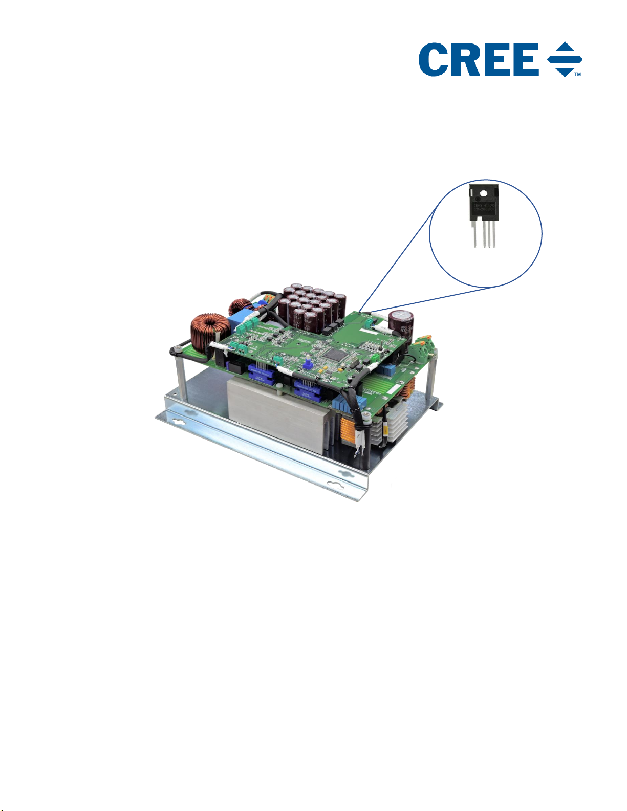
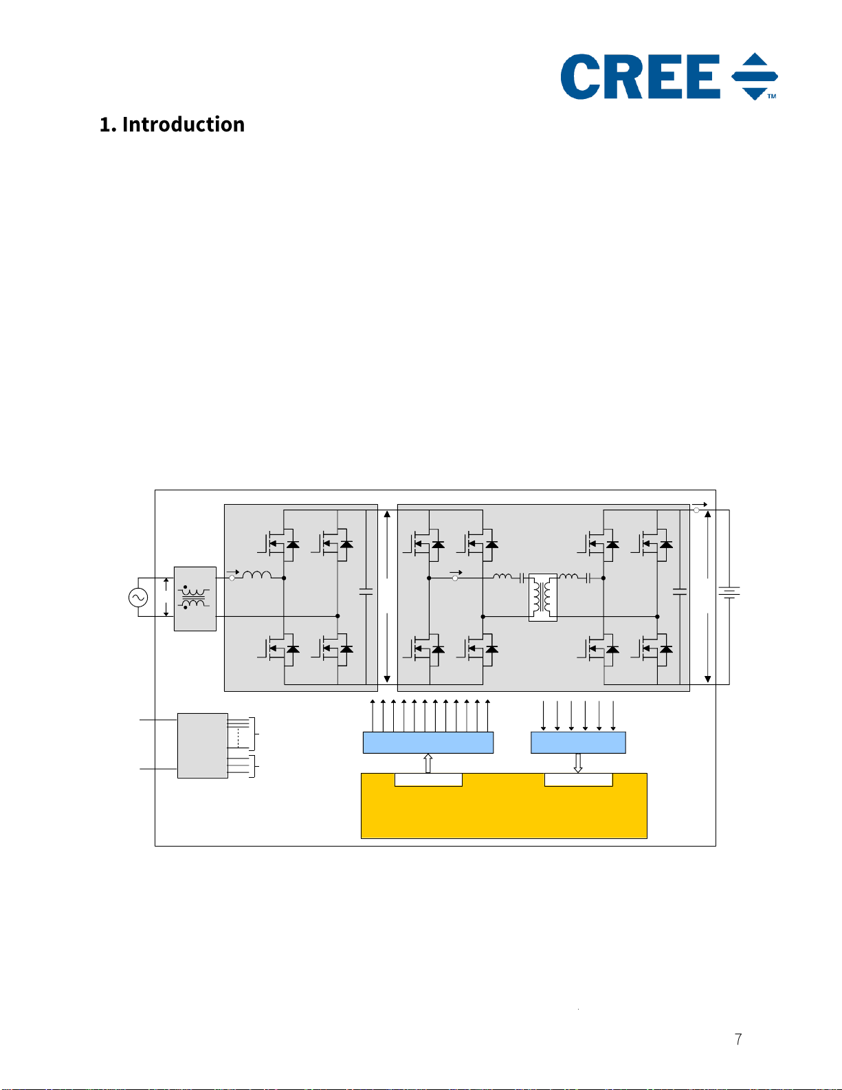
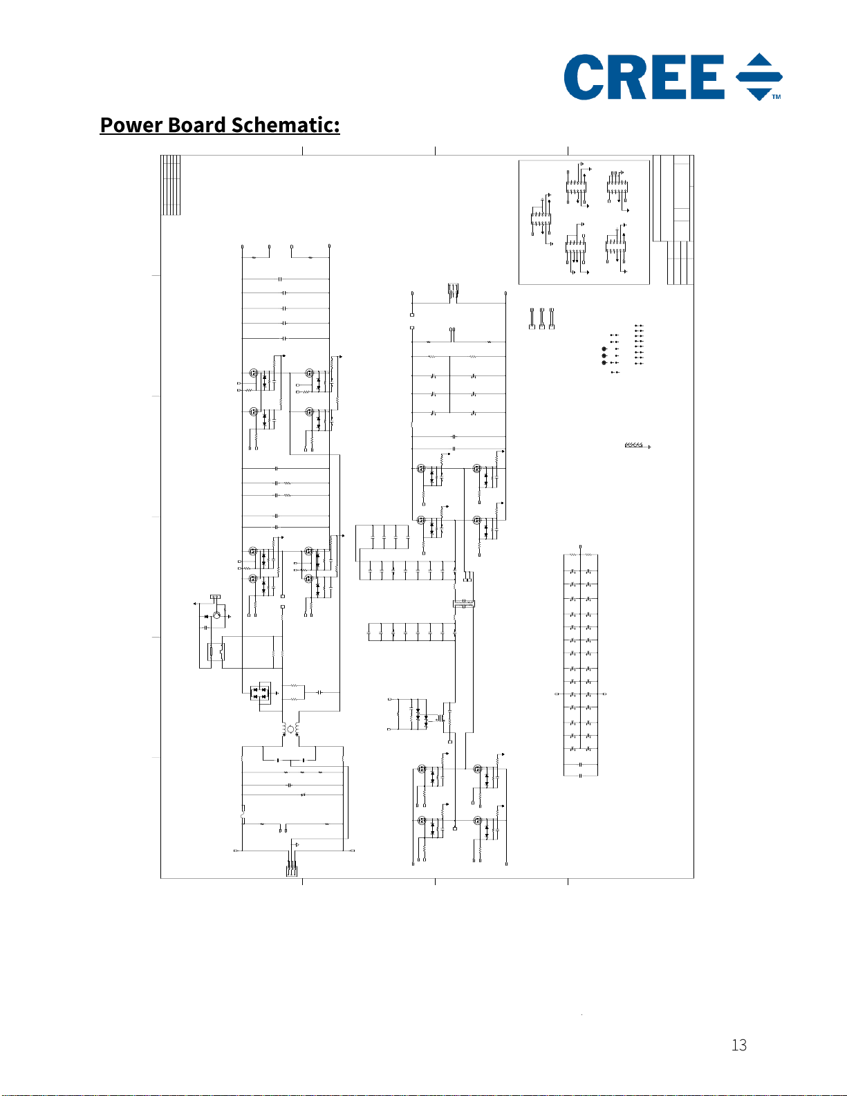
As shown in Figure 2, the Input AC voltage is connected to terminals 1 and 3 of CON5 followed
by the fuse F1 and MOV (Metal Oxide Varistor) RV1. Differential mode filters L1 and L2 and
common mode filter XL1 are then connected, and the filters are followed by a low frequency
rectifier BD1 which charges the output DC link capacitors through positive temperature
coefficient (PTC) resistors RV1 and RV2. RV1 and RV2 are shorted by relay, if the DC link voltage
crosses the peak value of the input grid voltage, then rectifier BD1 becomes reverse biased and
no current flows through the rectifier BD1. The main PFC inductor L3 is connected after the relay.
The other end of L3 is connected to the midpoint of the high frequency half bridge Totem-Pole
MOSFETs Q1, Q2, Q3, and Q4. After passing through the differential and common mode filters,
the neutral point of the grid is connected to the low frequency half bridge Q5, Q6, Q7, and Q8.
The DC link capacitor bank consists of 18 pieces of 250 µf, 400 V capacitors connected in series
and parallel combination. There are some film capacitors and RC snubber circuits as well to
absorb the high frequency ripple and reduce EMI (Electromagnetic Interference).
The DC link is connected to an H-bridge comprised of MOSFETs Q9, Q10, Q11, and Q12 which
forms the primary side of the bi-directional CLLC converter. The resonance tank is composed of
an inductor (L4) and a resonance capacitor bank of 12 pieces of 4.7nF film capacitor. The
inductance of main CLLC transformer is 100 µH with a PQ5050 core. The secondary side of
PQ5050 core is connected to the secondary side resonance inductor L5 and a bank of 18 pieces
of secondary side resonance capacitors. The secondary side H-bridge is composed of MOSFETs
Q13, Q14, Q15, and Q16 followed by film capacitors C58 and C59 and an electrolytic capacitor.
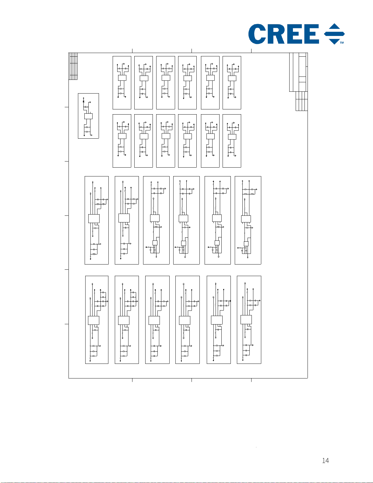
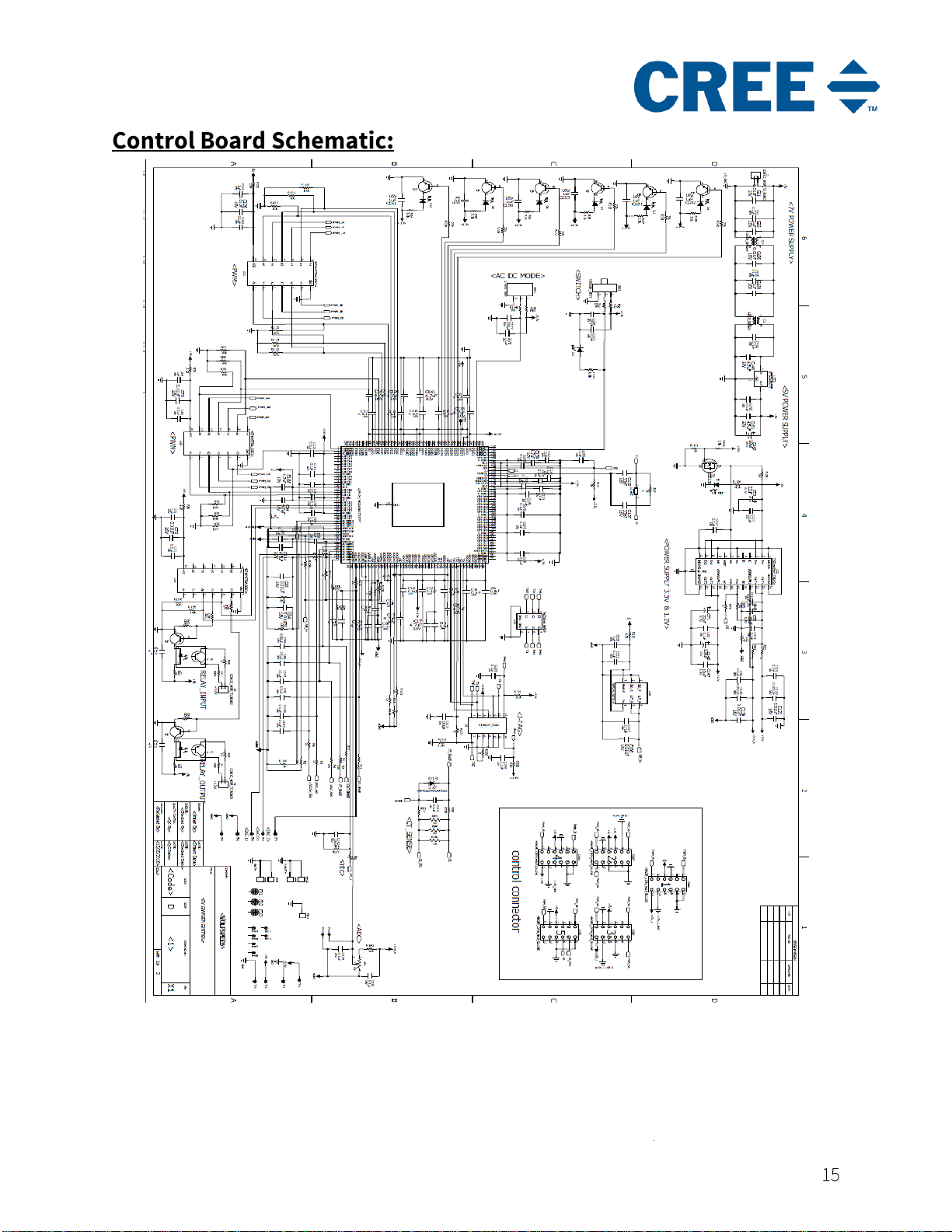
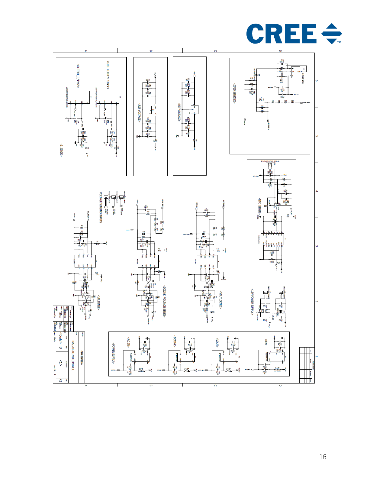
As shown in Figure 3, the gate drive signals for the MOSFETs of the PFC stage and the resonance
stage are generated by the DSP (Digital Signal Processing) controller and each MOSFET is further
isolated by their respective gate drivers. There are separate isolated DC/DC (VIN = +15, VOUT =
+15V, -3V) supplies for all gate drivers. The input currents and output load currents are sensed
by a current sensor for processing in the DSP controller. All voltage sensing (grid as well as the
output voltage) signals are isolated with an analog optocoupler before being fed into the DSP
controller for further processing.
CPWR-AN26, Rev A, 08-2018
Copyright © 2018 Cree, Inc. All rights reserved.
The information in this document is subject to change without notice.
Cree and Zero Recovery are registered trademarks, and the Cree logo and C3M are trademarks, of Cree, Inc
As shown in Figure 4 and Figure 5, the DSP controller from Texas Instruments Inc.
(P/N: TMS320F28337) is the main component of the control board carrying the control algorithm
of the whole system. The input of the control board is an isolated 7 V, 1 A power supply which is
regulated to +5V using a linear regulator. The 3.3 V and 1.2 V power supplies are further created
from the +5V supply using a precision regulator U22 from Texas Instruments Inc. (P/N: TPS70445).
All output PWM (Pulse Width Modulation) signals are buffered and shifted to +5V level by using
a Fairchild Semiconductor International Inc. level shifter (P/N: MC74HCT50A) and a buffer IC
(U13, U15, and U21) before being fed to their respective gate drivers. The reference for the ADC
(Analog to Digital Converter) of the DSP is generated through a precision reference IC (U18) from
Texas Instruments Inc. (P/N: REF3230AIDBVT). All incoming signals to the DSP such as voltages
and currents are galvanically isolated from the high-power side.
CPWR-AN26, Rev A, 08-2018
Copyright © 2018 Cree, Inc. All rights reserved.
The information in this document is subject to change without notice.
Cree and Zero Recovery are registered trademarks, and the Cree logo and C3M are trademarks, of Cree, Inc
CAUTION
IT IS NOT NECESSARY FOR YOU TO TOUCH THE BOARD WHILE IT IS ENERGIZED. WHEN
DEVICES ARE BEING ATTACHED FOR TESTING, THE BOARD MUST BE DISCONNECTED FROM
THE ELECTRICAL SOURCE AND ALL BULK CAPACITORS MUCH BE FULLY DISCHARGED.
SOME COMPONENTS ON THE BOARD REACH TEMPERATURES ABOVE 50OCELSIUS. THESE
CONDITIONS WILL CONTINUE AFTER THE ELECTRICAL SOURCE IS DISCONNECTED UNTIL THE
BULK CAPACITORS ARE FULLY DISCHARGED. DO NOT TOUCH THE BOARD WHEN IT IS
ENERGIZED AND ALLOW THE BULK CAPACITORS TO COMPLETELY DISCHARGE PRIOR TO
HANDLING THE BOARD.
PLEASE ENSURE THAT APPROPRIATE SAFETY PROCEDURES ARE FOLLOWED WHEN
OPERATING THIS BOARD AS SERIOUS INJURY, INCLUDING DEATH BY ELECTROCUTION OR
SERIOUS INJURY BY ELECTRICAL SHOCK OR ELECTRICAL BURNS, CAN OCCUR IF YOU DO NOT
FOLLOW PROPER SAFETY PRECAUTIONS.

Popular Batteries Charger manuals by other brands

Smappee EV Base installation manual

Smappee

Smappee EV Base installation manual

Intermec AC17 supplementary guide

Intermec

Intermec AC17 supplementary guide

Black & Decker BC2WBD instruction manual

Black & Decker

Black & Decker BC2WBD instruction manual

PROFECO 77419 instruction manual

PROFECO

PROFECO 77419 instruction manual

CELEKTRON CK7-132 user manual

CELEKTRON

CELEKTRON CK7-132 user manual

efacec EFAPOWER EV-QC45 Installation and user manual

efacec

efacec EFAPOWER EV-QC45 Installation and user manual

Staudte Hirsch SH-3.120 instruction manual

Staudte Hirsch

Staudte Hirsch SH-3.120 instruction manual

Parkside PAA 20-Li B2 Translation of the original instructions

Parkside

Parkside PAA 20-Li B2 Translation of the original instructions

XD XCLUSIVE XD P774.32X manual

XD XCLUSIVE

XD XCLUSIVE XD P774.32X manual

Wallbox QUASAR installation guide

Wallbox

Wallbox QUASAR installation guide

Magnetek MLTX instruction manual

Magnetek

Magnetek MLTX instruction manual

Haussmann 59595073 Operator's manual

Haussmann

Haussmann 59595073 Operator's manual

Voltr CHGFAST20 manual

Voltr

Voltr CHGFAST20 manual

Alpha A1-14-24-P User manual and installation guide

Alpha

Alpha A1-14-24-P User manual and installation guide

Super Start SPSS2-CA owner's manual

Super Start

Super Start SPSS2-CA owner's manual

Icy Box IB-CH101Q manual

Icy Box

Icy Box IB-CH101Q manual

Conrad FPS-3500/4 operating instructions

Conrad

Conrad FPS-3500/4 operating instructions

Milwaukee MXFCP203 Original instructions

Milwaukee

Milwaukee MXFCP203 Original instructions

manuals.online logo
manuals.online logoBrands
  • About & Mission
  • Contact us
  • Privacy Policy
  • Terms and Conditions

Copyright 2025 Manuals.Online. All Rights Reserved.