ECS P6VPA2T User manual

Preface
Copyright
This publication, including all photographs, illustrations and software,
is protected under international copyright laws, with all rights re-
served. Neither this manual, nor any of the material contained herein,
may be reproduced without written consent of the author.
Version 1.0
Disclaimer
The information in this document is subject to change without notice.
The manufacturer makes no representations or warranties with re-
spect to the contents hereof and specifically disclaims any implied
warranties of merchantability or fitness for any particular purpose.
The manufacturer reserves the right to revise this publication and to
make changes from time to time in the content hereof without obliga-
tion of the manufacturer to notify any person of such revision or
changes.
Trademark Recognition
Microsoft, MS-DOS and Windows are registered trademarks of Mi-
crosoft Corp.
MMX, Pentium, Pentium-II, Pentium-III, Celeron are registered
trademarks of Intel Corporation.
Other product names used in this manual are the properties of their
respective owners and are acknowledged.

ii
Federal Communications Commission (FCC)
This equipment has been tested and found to comply with the limits
for a Class B digital device, pursuant to Part 15 of the FCC Rules.
These limits are designed to provide reasonable protection against
harmful interference in a residential installation. This equipment gen-
erates, uses, and can radiate radio frequency energy and, if not
installed and used in accordance with the instructions, may cause
harmful interference to radio communications. However, there is no
guarantee that interference will not occur in a particular installation. If
this equipment does cause harmful interference to radio or television
reception, which can be determined by turning the equipment off
and on, the user is encouraged to try to correct the interference by
one or more of the following measures:
−Reorient or relocate the receiving antenna.
−Increase the separation between the equipment and the
receiver.
−Connect the equipment onto an outlet on a circuit different
from that to which the receiver is connected.
−Consult the dealer or an experienced radio/TV technician
for help.
Shielded interconnect cables and a shielded AC power cable must
be employed with this equipment to ensure compliance with the per-
tinent RF emission limits governing this device. Changes or
modifications not expressly approved by the system's manufacturer
could void the user's authority to operate the equipment.

iii
Declaration of Conformity
This device complies with part 15 of the FCC rules. Operation is sub-
ject to the following conditions:
−This device may not cause harmful interference, and
−This device must accept any interference received, includ-
ing interference that may cause undesired operation.
Canadian Department of Communications
This class B digital apparatus meets all requirements of the Cana-
dian Interference-causing Equipment Regulations.
Cet appareil numérique de la classe B respecte toutes les exigences
du Réglement sur le matériel brouilieur du Canada.

iv
About the Manual
The manual consists of the following:
Chapter 1
Introducing the Mainboard Describes features of the main-
board, and provides a shipping
checklist.
Go to ⇒page 1
Chapter 2
Installing the Mainboard Describes installation of main-
board components.
Go to ⇒page 9
Chapter 3
Using BIOS Provides information on using
the BIOS Setup Utility.
Go to ⇒page 33
Chapter 4
Using the Mainboard Software Describes the mainboard soft-
ware.
Go to ⇒page 67
Appendix A
Setting Jumpers Provides a reference to the
jumpers on the mainboard.
Go to ⇒page 75

v
T
TA
AB
BL
LE
E
O
OF
F
C
CO
ON
NT
TE
EN
NT
TS
S
Preface i
CHAPTER 1 1
Introducing the Mainboard 1
Introduction ...............................................................................1
Checklist...................................................................................1
Standard Items ................................................................................................1
Features ...................................................................................2
Mainboard Components.............................................................4
Jumper..............................................................................................................6
Choosing a Computer Case.......................................................7
CHAPTER 2 9
Installing the Mainboard 9
Safety Precautions.....................................................................9
Quick Guide ............................................................................ 10
Checking Jumper Settings........................................................ 11
Setting Jumpers ............................................................................................11
Checking Jumper Settings..........................................................................12
Jumper Settings............................................................................................13
Installing the Mainboard in a Case............................................ 14
Connecting Case Components ................................................. 15
The Panel Connector...................................................................................16
Installing Hardware .................................................................. 17
Installing the Processor...............................................................................17
Installing Memory Modules.......................................................................20
Installing a Hard Disk Drive/CD-ROM ...................................................22
Installing a Floppy Diskette Drive............................................................25
Installing Add-on Cards..............................................................................26
Connecting Optional Devices ....................................................................28
Connecting I/O Devices............................................................ 31
External Connector Color Coding.............................................................32
CHAPTER 3 33
Using BIOS 33
About the Setup Utility.............................................................. 33
The Standard Configuration.......................................................................34
Entering the Setup Utility...........................................................................35
Updating the BIOS.......................................................................................36

vi
Using BIOS ............................................................................. 37
Standard CMOS Features ...........................................................................37
Advanced BIOS Setup Option...................................................................40
Advanced Chipset Features Option...........................................................43
Integrated Peripherals Option ....................................................................48
Power Management Setup Option.............................................................54
PNP/PCI Configuration Option.................................................................59
Frequency/Voltage Control.........................................................................62
Load Fail-Safe Defaults Option.................................................................64
Load Optimized Defaults Option..............................................................64
Set Supervisor and User Passwords Options...........................................65
Save & Exit Setup Option...........................................................................66
Exit Without Saving.....................................................................................66
CHAPTER 4 67
Using the Mainboard Software 67
About the Software CD-ROM.................................................... 67
Auto-installing under Windows 98 ............................................. 68
Running Setup..............................................................................................69
Folders for this Mainboard........................................................ 71
Utility Folder.................................................................................................71
P6VPA2T Folder..........................................................................................71
Utility Folder Installation Notes.................................................. 72
Mainboard (P6VPA2T) Installation Notes................................... 73
Audio Drivers ...............................................................................................73
IDE Software ................................................................................................74
APPENDIX A 75
Setting Jumpers 75
Jumper Settings............................................................................................75
The Panel Connector...................................................................................77

C
Ch
ha
ap
pt
te
er
r
1
1
Introducing the Mainboard
I
In
nt
tr
ro
od
du
uc
ct
ti
io
on
n
Congratulations on purchasing the P6VPA2T mainboard. The
P6VPA2T mainboard is an ATX mainboard that uses a 4-layer
printed circuit board and measures 220 mm x 304 mm. The
mainboard features a Socket 370 that accommodates FC-
PGA Celeron, FC-PGA Pentium II/III and Tualatin processors
supporting frontside bus (FSB) speeds of 66/100/133 MHz.
The P6VPA2T incorporates the VIA Pro266T Northbridge and
VT8233 Southbridge chipsets which combine support for the
new high-bandwidth Double Data Rate (DDR) 266 SDRAM,
and the AC 97 audio codec.
Note: SDRAM provides 800 MBps or 1 GBps data trans-
fer depending on whether the bus is 100 MHz or
133 MHz. Double Data Rate SDRAM (DDR
SDRAM) doubles the rate to 1.6 GBps or 2.1 GBps
by transferring data on both the rising and falling
edges of the clock. DDR SDRAM uses additional
power and ground lines and requires 184-pin DIMM
modules rather than the 168-pin DIMMs used by
SDRAM.
C
Ch
he
ec
ck
kl
li
is
st
t
Compare the mainboard’s package contents with the following
checklist:
Standard Items
•One mainboard
•One diskette drive ribbon cable and bracket
•One IDE drive ribbon cable and bracket
•Software support CD
•This user’s manual
2
F
Fe
ea
at
tu
ur
re
es
s
Processor The P6VPA2T mainboard includes a Socket 370
that has the following features:
•Supports up to a 133 MHz frontside bus (FSB)
•Accommodates FC-PGA Celeron, FC-PGA
Pentium III/Tualatin, and Cyrix III processors.
Chipset The VIA Pro266T Northbridge and Southbridge
chipsets are based on an innovative and scaleable
architecture with proven reliability and performance.
A few of the chipset’s advanced features are:
•An advanced V-Link memory controller archi-
tecture that provides the bandwidth and
performance necessary for even the most
demanding Internet and 3D graphics
•A low 2.5-volt DDR266 SDRAM power con-
sumption which makes it an excellent solution
for notebooks and desktops with a small foot-
print
•Support for a 4xAGP interface providing vivid
3D graphics and video performance
•An ATA 100 interface on the chipset, which
helps boost system performance by providing
a high-speed connection to ATA 100 Hard
Disk Drives, delivering maximum sustained
data transfer rates of 100 MB/sec
Additional key features include support for six
USB ports, an AC 97 link for audio and HSP mo-
dem, and ACPI/OnNow power management.
Memory The mainboard accommodates DDR200/266
(PC1600/PC2100) DDR SDRAM (Double Data
Rate Synchronous DRAM) up to 3 GB using three
2.5V unbuffered DIMM modules.
VGA The P6VPA2T includes a 4xAGP slot that pro-
vides four times the bandwidth of the original AGP
specification. AGP technology provides a direct
connection between the graphics sub-system and
the processor so that the graphics do not have to
compete for processor time with other devices on
the PCI bus.

3
AC 97 Audio
Codec The AC 97 Audio codec is compliant with the AC
97 2.1 specification, and supports 18-bit ADC
(Analog Digital Converter) and DAC (Digital Ana-
log Converter) resolution as well as 18-bit stereo
full-duplex codec with independent and variable
sampling rates. Further features include support
for four analog line-level stereo inputs.
Expansion
Options P6VPA2T has six 32-bit PCI slots, an AGP slot,
and a CNR (Communications Networking Riser)
slot. The P6VPA2T PCI slots are capable of Ultra
DMA33/66 bus mastering.
Integrated I/OThe mainboard has a full set of I/O ports and con-
nectors:
•Two PS/2 ports for mouse and keyboard
•Two serial port
•One parallel port
•One MIDI/game port
•Six USB ports (2 backpanel ports, onboard
USB headers providing 4 extra ports)
•Audio jacks for microphone, line-in and line-
out
BIOS
Firmware This mainboard uses Award BIOS that enables
users to configure many system features including
the following:
•Power management
•CPU and memory timing
•Modem wake up alarms
The firmware can also be used to set parameters
for different processor clock speeds.

4
M
Ma
ai
in
nb
bo
oa
ar
rd
d
C
Co
om
mp
po
on
ne
en
nt
ts
s
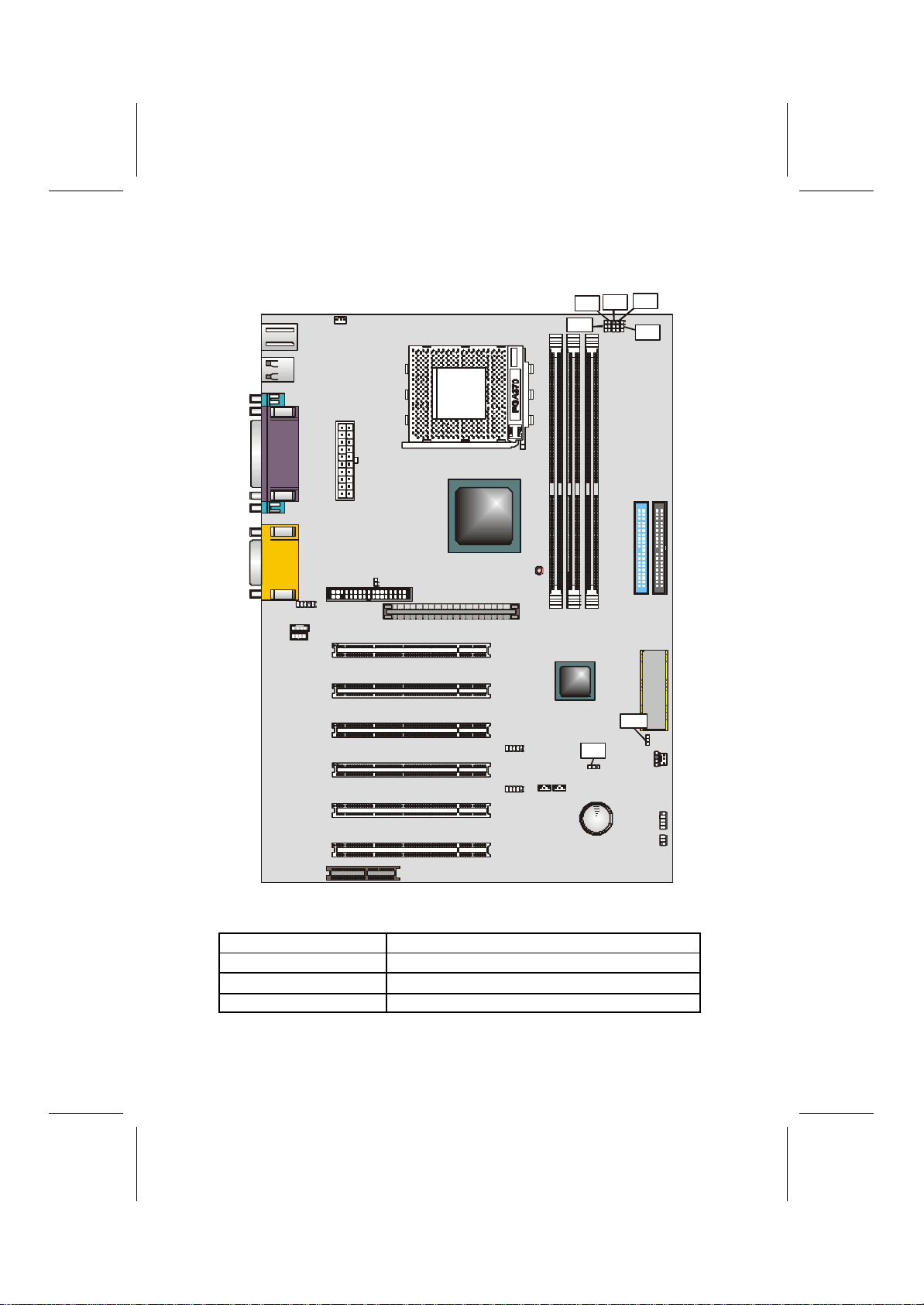
CPUFAN1
CASFAN1
DIM1 DIM2 DIM3
LED1
IDE2
ATX1
J1
CASEOPEN1
CD1
AGP1
PCI1
PCI2
PCI3
PCI4
PCI5
PCI6
CNR1
BT1
USB2
USB3
JP2
WOL1 WOM1
SPEAKER1
PANEL1
SIR1
FDD1
CD2
IDE1
JP1
JP3 JP4JP5 JP6JP7
1
1 1 1 1 1
1
1
11
1
1
1AGP1
PCI1
PCI2
PCI3
PCI4
PCI6
PCI5
CNR1
BT1
USB2
USB3 WOL1
WOM1
SIR1
PANEL1
SPEAKER1
LED1
IDE1 IDE2
DIM3
DIM2
DIM1
CPU SOCKET
CPUFAN1
ATX1
CD1
CD2
J1
CASFAN1
CASEOPEN1
FDD1

5
Table of Mainboard Components
Label Component
AGP1 Accelerated Graphics Port
ATX1 Power connector
BT1 Three volt realtime clock battery
CASEOPEN1 Used for case open switch
CASFAN1 Auxiliary case cooling fan
CD1 Primary CD-in connector
CD2 Secondary CD-in connector
CNR1 Communications Network Riser (CNR) slot
CPU SOCKET PGA370 CPU Socket
CPUFAN1 Cooling fan for CPU
DIM1 ~ DIM3 Three 184-pin DIMM sockets
FDD1 Floppy disk drive connector
IDE 1 Primary IDE channel
IDE 2 Secondary IDE channel
J1 Front panel audio
LED1 2.5 VSB for SDRAM
PANEL1 Connector for case front panel switches and
LED indicators
PCI1 ~ PCI6 Six 32-bit add-in card slots
SIR1 Serial infrared cable header
SPEAKER1 Speaker connector
USB2 Connector for front panel USB ports
USB3 Connector for front panel USB ports
WOL1 Wake On LAN wakeup connector
WOM1 Wake On Modem wakeup connector
Note: LED1 -This red indicator warns you that the com-
puter is still powered on and you should not install
or uninstall memory modules.
6
Jumper
CPUFAN1
CASFAN1
DIM1 DIM2 DIM3
LED1
IDE2
ATX1
J1
CASEOPEN1
CD1
AGP1
PCI1
PCI2
PCI3
PCI4
PCI5
PCI6
CNR1
BT1
USB2
USB3
JP2
WOL1 WOM1
SPEAKER1
PANEL1
SIR1
FDD1
CD2
IDE1
JP1
JP3JP4 JP5JP6JP7
1
1 1 1 1 1
1
1
11
1
1
1
JP1
JP2
JP4
JP7
JP5
JP6
JP3
Table of Jumpers
Label Component
JP1 BIOS protection jumper
JP2 Clear CMOS jumper
JP3 ~ JP7 CPU Vcore adjustment jumper

7
C
Ch
ho
oo
os
si
in
ng
g
a
a
C
Co
om
mp
pu
ut
te
er
r
C
Ca
as
se
e
There are many types of computer cases on the market. The
mainboard complies with the specifications for the ATX sys-
tem case. Some features on the mainboard are implemented
by cabling connectors on the mainboard to indicators and
switches on the system case. Ensure that your case supports
all the features required. The mainboard can support two CD
drives, one floppy diskette drive and four enhanced IDE drives.
Ensure that your case has sufficient power and space for all
the drives that you intend to install.
Most cases have a choice of I/O templates in the rear panel.
Make sure that the I/O template in the case matches the I/O
ports installed on the rear edge of the mainboard.
This mainboard has an ATX form factor of 220 x 304 mm.
Choose a case that accommodates this form factor.
This concludes Chapter 1. The next chapter explains how to
install the mainboard.

8
—
Notes
—

C
Ch
ha
ap
pt
te
er
r
2
2
Installing the Mainboard
S
Sa
af
fe
et
ty
y
P
Pr
re
ec
ca
au
ut
ti
io
on
ns
s
Follow these safety precautions when installing the mainboard:
•Wear a grounding strap attached to a grounded device
to avoid damage from static electricity.
•Discharge static electricity by touching the metal case
of a safely grounded object before working on the
mainboard.
•Leave components in the static-proof bags they came
in.
•Hold all circuit boards by the edges. Do not bend cir-
cuit boards.

10
Q
Qu
ui
ic
ck
k
G
Gu
ui
id
de
e
This Quick Guide suggests the steps you can take to assem-
ble your system with the mainboard.
The following table provides a reference for installing specific
components:
Locating Mainboard Components Go to page 4
Setting Jumpers Go to page 11
Installing the Mainboard in a Case Go to page 14
Installing Case Components Go to page 15
Installing the CPUGo to page 17
Installing Memory Go to page 20
Installing an HDD and CD-ROM Drive Go to page 21
Installing an FDD Go to page 25
Installing Add-on Cards Go to page 26
Connecting Options Go to page 28
Connecting Peripheral (I/O) Devices Go to page 31
Note: The appendix provides a quick reference for jumper
settings.

11
C
Ch
he
ec
ck
ki
in
ng
g
J
Ju
um
mp
pe
er
r
S
Se
et
tt
ti
in
ng
gs
s
This section explains how to set jumpers for correct configura-
tion of the mainboard.
Setting Jumpers
Use the mainboard jumpers to set system configuration op-
tions. Jumpers with more than one pin are numbered. When
setting the jumpers, ensure that the jumper caps are placed
on the correct pins.
Short Open
This illustration shows a 2-pin
jumper. When the jumper cap is
placed on both pins, the jumper is
SHORT. If you remove the jumper
cap, or place the jumper cap on
just one pin, the jumper is OPEN.
123
This illustration shows a 3-pin
jumper. Pins 1 and 2 are SHORT.
12
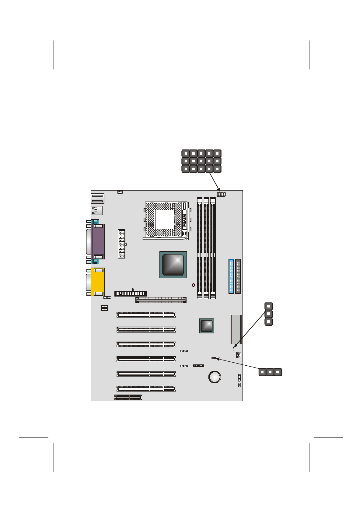
Checking Jumper Settings
The following illustration shows the location of the mainboard
jumpers. Pin 1 is labeled.
CPUFAN1
CASFAN1
DIM1 DIM2 DIM3
LED1
IDE2
ATX1
J1
CASEOPEN1
CD1
AGP1
PCI1
PCI2
PCI3
PCI4
PCI5
PCI6
CNR1
BT1
USB2
USB3
JP2
WOL1 WOM1
SPEAKER1
PANEL1
SIR1
FDD1
CD2
IDE1
JP1
JP3JP4JP5JP6JP7
1
111 11
1
1
11
1
1
1
JP3
JP7
JP5
JP6
JP4
JP2
JP1
11111
1
1

13
Jumper Settings
Jumper Type Description Setting (default)
JP1 3-pin BIOS flash
protection
jumper
1-2: Disable
2-3: Enable JP1
1
JP2 3-pin Clear CMOS
jumper 1-2: Normal
2-3: Clear CMOS JP2
1
JP3
JP4
JP5
JP6
JP7
3-pin CPU core
voltage select
jumper
Refer to the
table on page
76 for pin
information.
JP3
1
JP4JP5 JP6JP7
JP1: BIOS Flash Protect Jumper
This jumper is used to protect the BIOS from being uninten-
tionally flashed. Enable this jumper for protection and disable
this jumper when you want to flash the BIOS.
JP2: Clear CMOS Jumper
This jumper enables you to reset the BIOS. Follow these
instructions to reset the BIOS:
1. Turn the system off.
2. Short pins 2 and 3 on JP2.
3. Return the jumper to the normal setting.
4. Turn the system on. The BIOS is returned to the de-
fault settings.
Jumper 3 ~ 7: CPU Vcore adjust jumper
Use these 3 X 1 pin jumpers to manually set the CPU core
voltage.
Refer to the table in Appendix A for more information.

14
I
In
ns
st
ta
al
ll
li
in
ng
g
t
th
he
e
M
Ma
ai
in
nb
bo
oa
ar
rd
d
i
in
n
a
a
C
Ca
as
se
e
Refer to the following illustration and instructions for installing
the mainboard in a case:
This illustration shows
an example of a main-
board being installed in
a tower-type case:
Note: Do not over-
tighten the
screws as this
can stress the
mainboard.
Most system cases have
mounting brackets in-
stalled in the case,
which correspond to the
holes in the mainboard.
Place the mainboard
over the mounting
brackets and secure the
mainboard onto the
mounting brackets with
screws.
2. Secure the mainboard with
screws where appropriate.
1. Place the mainboard
over the mounting brackets.
Ensure that your case has an I/O template that supports the
I/O ports and expansion slots on your mainboard.
Table of contents
Other ECS Motherboard manuals


