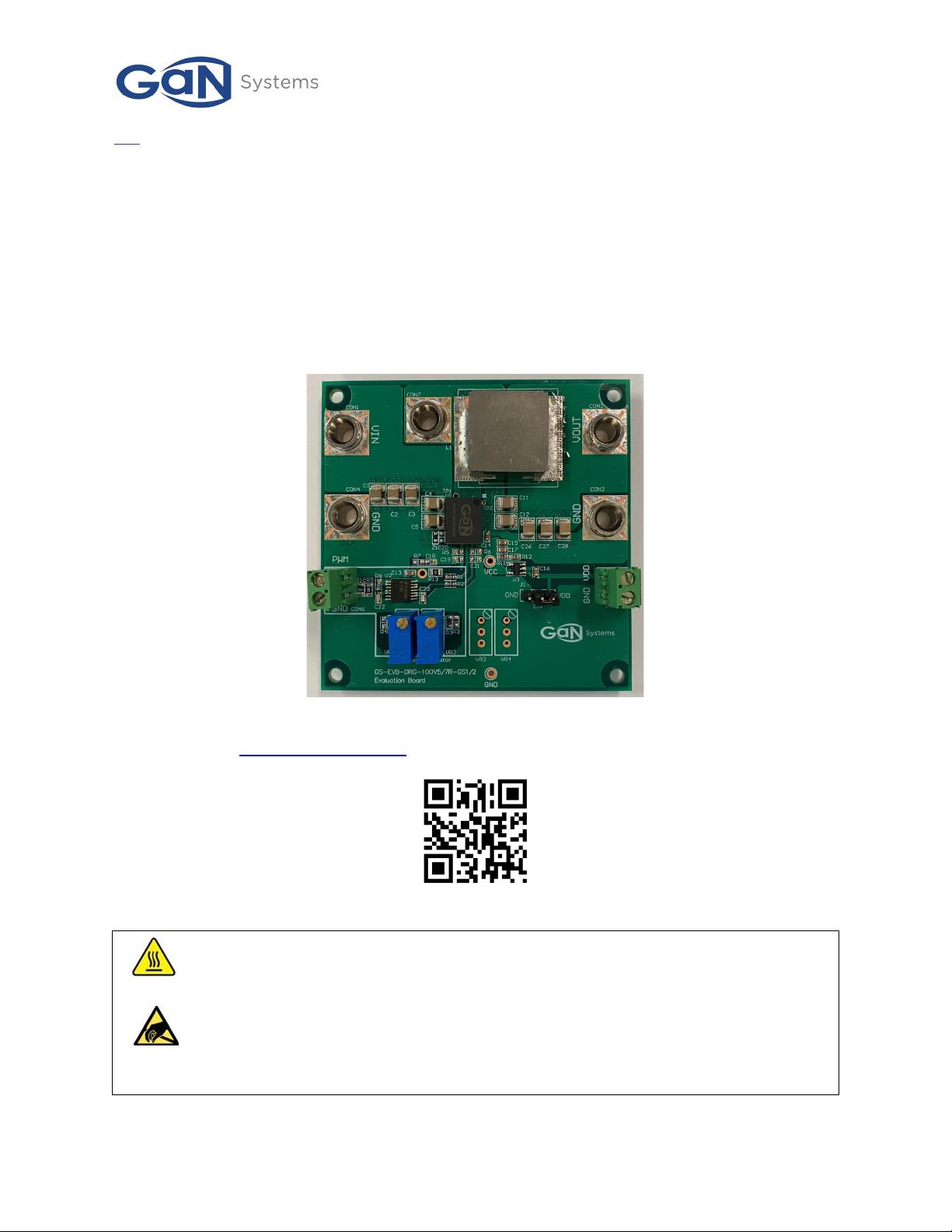
GS-EVB-DRG-100V7R-GS2
100 V Driver GaN Open Loop Buck/Boost
Evaluation Board Technical Manual
___________________________________________________________________________________________________________________
GS-EVB-DRG-100V7R-GS2 TM Rev. 201013 © 2020 GaN Systems Inc. www.gansystems.com 10
Please refer to the Evaluation Board/Kit Important Notice on page 10
Evaluation Board/kit Important Notice
GaN Systems Inc. (GaN Systems) provides the enclosed product(s) under the following AS IS conditions:
This evaluation board/kit being sold or provided by GaN Systems is intended for use for ENGINEERING
DEVELOPMENT, DEMONSTRATION, and OR EVALUATION PURPOSES ONLY and is not considered by GaN
Systems to be a finished end-product fit for general consumer use. As such, the goods being sold or provided are
not intended to be complete in terms of required design-, marketing-, and/or manufacturing-related protective
considerations, including but not limited to product safety and environmental measures typically found in end
products that incorporate such semiconductor components or circuit boards. This evaluation board/kit does not fall
within the scope of the European Union directives regarding electromagnetic compatibility, restricted substances
(RoHS), recycling (WEEE), FCC, CE or UL, and therefore may not meet the technical requirements of these directives,
or other related regulations.
If this evaluation board/kit does not meet the specifications indicated in the Technical Manual, the board/kit may be
returned within 30 days from the date of delivery for a full refund. THE FOREGOING WARRANTY IS THE
EXCLUSIVE WARRANTY MADE BY THE SELLER TO BUYER AND IS IN LIEU OF ALL OTHER WARRANTIES,
EXPRESSED, IMPLIED, OR STATUTORY, INCLUDING ANY WARRANTY OF MERCHANTABILITY OR FITNESS
FOR ANY PARTICULAR PURPOSE. EXCEPT TO THE EXTENT OF THIS INDEMNITY, NEITHER PARTY SHALL
BE LIABLE TO THE OTHER FOR ANY INDIRECT, SPECIAL, INCIDENTAL, OR CONSEQUENTIAL DAMAGES.
The user assumes all responsibility and liability for proper and safe handling of the goods. Further, the user
indemnifies GaN Systems from all claims arising from the handling or use of the goods. Due to the open construction
of the product, it is the user’s responsibility to take any and all appropriate precautions with regard to electrostatic
discharge.
No License is granted under any patent right or other intellectual property right of GaN Systems whatsoever. GaN
Systems assumes no liability for applications assistance, customer product design, software performance, or
infringement of patents or any other intellectual property rights of any kind.
GaN Systems currently services a variety of customers for products around the world, and therefore this
transaction is not exclusive.
Please read the Technical Manual and, specifically, the Warnings and Restrictions notice in the Technical
Manual prior to handling the product. Persons handling the product(s) must have electronics training and
observe good engineering practice standards.
This notice contains important safety information about temperatures and voltages. For further safety concerns,
please contact a GaN Systems’ application engineer.