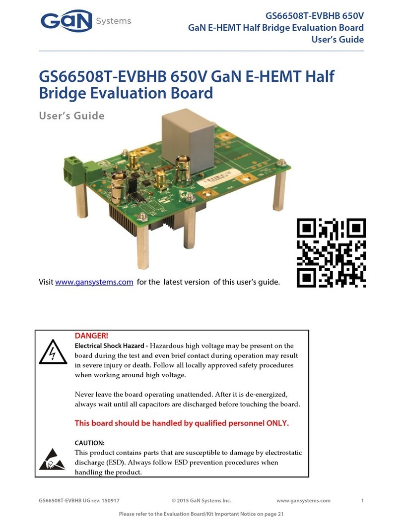
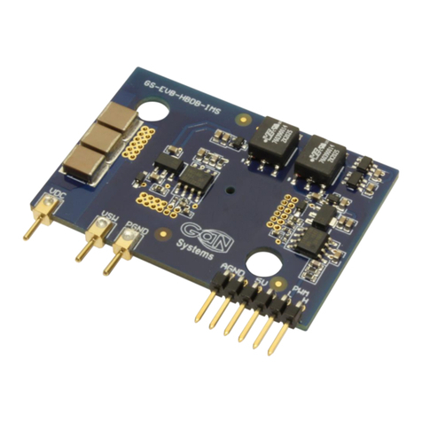
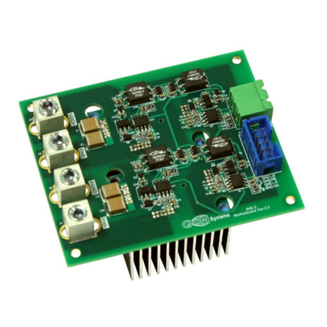
Gan Systems GS66502B-EVBDB User manual

Visit www.gansystems.com for the latest version of this user’s guide.
This evaluation kit is designed for engineering evaluation in a controlled
lab environment and should be handled by qualified personnel ONLY.
High voltage will be exposed on the board during the test and even brief
contact during operation may result in severe injury or death.
Never leave the board operating unattended. After it is de-energized,
always wait until all capacitors are discharged before touching the board.
This product contains parts that are susceptible to damage by electrostatic
discharge (ESD). Always follow ESD prevention procedures when
handling the product.

The GS665XXX-EVBDB daughter board style evaluation kit consists of two GaN Systems 650V GaN
Enhancement-mode HEMTs (E-HEMTs) and all necessary circuits including half bridge gate drivers,
isolated power supplies and optional heatsink to form a functional half bridge power stage. It allows
users to easily evaluate the GaN E-HEMT performance in any half bridge-based topology, either with the
universal mother board (P/N: GS665MB-EVB) or users’ own system design for quick prototyping.
Serves as a reference design and evaluation tool as well as deployment-ready solution for easy in-
system evaluation.
Vertical mount style with height of 35mm, which fits in majority of 1U design and allows
evaluation of GaN E-HEMT in traditional through-hole type power supply board.
Current shunt position for switching characterization testing
Universal form factor and footprint for all products
The daughter board and universal mother board ordering part numbers are below:
Part Number
GaN E-HEMT P/N:
Description
GS66502B-EVBDB
GS66502B
GaN E-HEMT 650V/7.5A, 200mΩ
GS66504B-EVBDB
GS66504B
GaN E-HEMT 650V/15A, 100mΩ
GS66508B-EVBDB
GS66508B
GaN E-HEMT 650V/30A, 50mΩ
GS66508T-EVBDB
GS66508T
GaN E-HEMT top side cooled 650V/30A, 50mΩ
GS66516T-EVBDB
GS66516T
GaN E-HEMT top side cooled 650V/60A, 25mΩ
GS665MB-EVB
GS665MB-EVB
Universal 650V Mother Board
The daughter board GS665XXX-EVBDB circuit diagram is shown in Figure 1. The control logic inputs on
2x3 pin header J1 are listed below:
Pin
Descriptipon
ENA
Enable input. It is internally pulled up to VCC, a low logic disables all the PWM gate
drive outputs.
VCC
+5V auxillary power supply input for logic circuit and gate driver. On the daughter
board there are 2 isolated 5V to 9V DC/DC power supplies for top and bottom switches.
VDRV
Optional 9V gate drive power input. This pin allows users to supply separate gate drive
power supply. By default VDRV is connected to VCC on the daughter board via a 0 ohm
jumper FB1. If bootstrap mode is used for high side gate drive, connect VDRV to 9V
PWMH
High side PWM logic input for top switch Q1. It is compatible wth 3.3V and 5V
PWML
Low side PWM logic input for bottom switch Q2. It is compatible wth 3.3V and 5V
0V
Logic inputs and gate drive power supply ground return.
The 3 power pins are:
VDC+: Input DC Bus voltage
VSW: Switching node output
VDC-: Input DC bus voltage ground return. Note that control ground 0V is isolated from VDC-.
Si8271 Iso.
Gate Driver Q1
Q2
Si8271 Iso.
Gate Driver
Iso. DC/DC
or Bootstrap
Iso. DC/DC
VDC+
VSW
VDC-
VCC
ENABLE
JP1
C4-10
PWMH
PWML

A. 2x GaN Systems 650V E-HEMT GS66508T(30A/50mΩ) or GS66516T (60A/25 mΩ). The PCB
footprints are universal and compatible for both packages
B. 5V-9V isolated DC/DC gate drive power supply
C. Decoupling capacitors C4-C11
D. Isolated gate driver Silab Si8271
E. Optional current shunt position JP1.
F. Test points for bottom Q2 VGS.
G. Recommended probing positions for Q2 VDS.
H. Holes for temperature monitoring of Q1/Q2
I. M3 mounting screw for heatsink
J. (Optional) RC snubber circuit
This daughter board includes two GaN Systems E-HEMT GS66508T (650V/30A, 50mΩ) or
GS66516T (650V/60A, 25mΩ) in a GaNPx™ Top cooled T type package, . The thermal pad on the
top of device is internally connected to the source. Electrical insulation will be needed for
heatsink attachment. GaNPx™ T package also features dual symmetrical gate for easier
paralleling and PCB layout.

Bipolar gate drive bias with +6V and -3V for turning off is chosen for this design for more robust
gate drive and better noise immunity.
5V-9V isolated DC/DC converters are used for gate drive. 9V is then splited into +6V and -3V bias
by using 6V Zener diode
By default gate drive supply input VDRV is tied to VCC +5V via 0Ωjumper (FB1). Remove FB1 if
separate gate drive input voltage is to be used.
Silab SI8271-GB-IS (3V UVLO) or SI8271–AB-IS (5V UVLO) isolated gate driver can be used for
this design. Both drivers are compatible with 6V/-3V gate drive and has CMTI dv/dt immunity
up to 200V/ns. It has separated source and sink drive outputs which eliminates the need for
additional diode.
GaN E-HEMT switching speed and slew rate can be directly controlled by the gate resistors. By
default the turn-on Rgate (R6/R12) is 10Ωand Rg_off (R7/R14) is 2Ω. User can adjust the values
of gate resistors to fine tune the turn-on and off speed.
FB1/FB2 are footprints for optional ferrite bead. By default they are populated with 0Ωjumpers.
If gate oscillation is observed, it is recommended to replace them with ferrite bead with Z=10-
20Ω@100MHz.
RS1/CS1 and RS2/CS2 are place holders to allow user to experiement with RC snubber circuit (not
installed). At high frequency operation the power dissipation for RS1/RS2 needs to be closely watched
and CS1/CS2 should be sized correctly. It is recommended to start with 33-47pF and 10-20Ω.
PS2
PES1-S5-S9-M
GND
1
VIN
2+VO 5
0V 4
NC
8
0V
VDRV
C14
4.7uF
C0805
VDDL_+6V
C15
4.7uF
C0805
GNDL
C16
4.7uF
C0805
R9
3.3K
LED2
LED-0603
U4
SI8271GB-IS
VI
1
VDDI
2
GNDI
3
EN
4GNDA 5
VO- 6
VO+ 7
VDD 8
PWML
DZ2
6.2V
SOD323-AC
AC
R16
1K
VEEL GNDL
C21
4.7uF
C0805
GNDL
C22
1uF GNDL
VEEL
JP1
CON-JMP-CSHUNT
R10
3.3K
R11
10R
PWML_IN
PGND
Q2S
Q2A
GS66508T
1
2
4
3
Q2B
GS66516T
1
2
43
ENABLE
Q2G2
R13
3.3K
Q2G
FB3
0R
R12
10R
R14
2R
Q2_GOUTQ2_VO+
RS2
10R
R1206
Q2_VO-
C17
1uF CS2
200p
C1206
DNP
DNP
VDDL_+6V
C18
1uF
0V
VCC_+5V

The board provides an optional current shunt position JP1 between the source of Q2 and power
ground return. This allows drain current measurement for switching characterization test such as
Eon/Eoff measurement.
The JP1 footprint is compatible with T&M Research SDN series coaxial current shunt
(recommended P/N: SDN-414-10, 2GHz B/W, 0.1Ω)
If current shunt is not used JP1 must be shorted. JP1 affects the power loop inductance and its
inductance should be kept as low as possible. Use a copper foil or jumper with low inductance.
1. When measuring VSW with current shunt, ensure all channel probe grounds and current shunt
BNC output case are all referenced to the source end of Q2 before the current shunt. The
recommended setup of probes is shown as below.
2. The output of coaxial current shunt can be connected to oscilloscope via 50Ωtermination
impedance to reduce the ringing.
3. The measured current is inverted and can be scaled by using: Id=Vid/Rsense.
Current
Shunt
Q2 Source VDC-

1. GS66508T or GS66516T has a thermal pad at the top side for improved heat dissipation. Instead
of relying on PCB for cooling, the heat can be transferred to heatsink directly from the top
reducing the total thermal resistnace.
2. A heatsink can be mounted to the board using a M3 screw with lock washer and nylon insulated
bushing. Thermal Interface Material (TIM) is needed to provide electrical insulation and
conformance to the thermal pad surface. The daughter board evaluation kit supplies with a
35x35mm heatsink with M3 tapped hole, and other heatsinks can also be used to fit users’ system
design.
3. Care should be taken during the assembly of heatsink to avoid PCB bending and mechanical
stress to the GaN E-HEMT. We recommend to limit the torque of M3 mounting screw to <1 in-lb
(0.1Nm) for GS66508T and <2 in-lb (0.2Nm) for GS66516T, which translates to about ~50psi
pressure on each device.
4. To measure device case temperature, use IR camera or install thermocouple to monitor the
temperature through two drilled holes from the top side as shown below:
VGL
VSL
VSW
BNC case
To oscilloscope
probe input (use
50Ω termination)
BNC tip
VDS
VGS
ID

°
5. The TIM we use on this assembly is Berguist®SilPad 1500ST, the measured total thermal
resistance can be found in Figure 9. Compared to bottom cooled design, T package eliminates the
PCB thermal resistance and significantly improve the thermal performance. Theraml grease is
typically not needed on the assembly. If thermal grease is to be applied, use non-conductive and
non-capacitive type thermal grease.
6. Forced air cooling is recommended for power testing.

GaNPX T GaNPX T
FR4 PCB
Heatsink
M3 Screw
Lock Washter
Insulated bushing
TIM

GaN Systems provides a universal 650V mother board (ordering part number: GS665MB-EVB, sold
separately) that can be used as the basic evaluation platform for all the daughter boards.
The universal 650V mother board evaluation kit includes following items:
1. Mother board GS665MB-EVB
2. 12VDC Fan
The board can be powered by 9-12V on J1. On-board voltage regulator creates to 5V for daughter board
and control logic circuits. J3 is used for external 12VDC fan.
12V INPUT
(+)5V Power Supply
CIN
VSW
PWM control & dead
time circuit
Daughter Board
Probing point for VSW
For Ext.
12VDC Fan
Airflow direction
Optional Cout
VDC- VOUT
VDC-
VDC+

The top and bottom switches PWM inputs can be individually controlled by two jumpers J4 and J6. Users
can choose between a pair of complementary on-board internal PWM signals (non-inverted and inverted,
controlled by J7 input) with dead time or external high/low side drive signals from J5 (users’ own control
board).
An on-board dead time generation circuit is included on the mother board. Dead time is controlled by
two RC delay circuits, R6/C12 and R5/C11. The default dead time is set to about 100ns. Additionally two
potentiometers locations are provided (TR1/TR2, not included) to allow fine adjustment of the dead time
if needed.
0V
D1 PMEG2005EB
SOD523
R6
1K00
TR12K C11
100pF
0V
R5
1K00
C10
1uF
C9
0.1uF
+5V
J7
112538 1
2
3
4
5
R4
100R
R1206
R2
100R
R1206
U2A
74VHC132
3
1
2
14
7
0V
R1
49R9 0V
D2 PMEG2005EB
SOD523
TR22K
C12
100pF
0V
U2B
74VHC132
4
56
U2C
74VHC132
9
10 8
U2D
74VHC132
12
13 11
TP7
TP8
DNP
DNP
PWM
OUTPUT
INVERTED
PWM OUTPUT
R3
49R9
DNP
DNP
R7
49R9

Test points are designed in groups/pairs to facilitate probing:
Test points
Name
Description
TP1/TP2
+5V/0V
5V bias power
TP7/TP8
PWMIN/0V
PWM input signal from J7
TP4/TP3/TP13
PWMH/PWML/0V
High/low side gate signals to daughter board
TP9/TP10
VDC+/VDC-
DC bus voltage
TP11/TP12
VOUT/VDC-
Output voltage
TP6/TP5
VSW/VDC-
Switching node output voltage (for HV oscilloscope
probe)
CON1-CON7 mounting pads are designed to be compatible with following mounting terminals:
#10-32 Screw mount,
Banana Jack PCB mount (Keystone P/N: 575-4), or
PC Mount Screw Terminal (Keystone P/N: 8191)
An external power inductor (not included) can be connected between VSW (CON1) and VOUT (CON4/5)
or VDC+ (CON2/3) for double pulse test. Users can choose their inductor size to meet the test
requirement. Generally it is recommended to use power inductor with low inter-winding capacitance to
obtain best switching performance. For the double pulse testing we use 2x 60uH/40Amp inductor (CWS,
P/N: HF467-600M-40AV) in series. C14 is designed to accommodate a film capacitor as output filter.

CON1
Q1
CON2
Q2
VDC-
CON4
CON3
LOUT
400V DC
+
VDC+
CON7CON6
VSW CON5
+5V
0V
PWM
INPUT
(J7)
VDS
IL
ISW
VGL
+6V
0VVDS
VGL
IL
t0 t1 t2 t3
TON1
Double pulse test allows easy evaluation of device switching performance at high voltage/current
without the need of actually running at high power. It can also be used for switching loss (Eon/Eoff)
measurement and other switching characterization parameter test.
The circuit configuration and operating principle can be found in Figure 14:
1. The output inductor is connected to the VDC+.
2. At t0 when Q2 is switched on, the inductor current starts to ramp up until t1. The period of first
pulse Ton1 defines the switching current ISW = (VDS*TON1) / L.
3. t1-t2 is the free wheeling period when the inductor current ILforces Q1 to conduct in reverse.
4. t1 (turn-off) and t2 (turn-on) are of interest for this test as they are the hard switching trasients for
the half bridge circuit when Q2 is under high switching stress.
5. The second pulse t2-t3 is kept short to limit the peak inductor current at t3.
The double pulse signal can be generated using programmable signal generaotor or microcontroller/DSP
board. As this test involves high switching stress and high current, it is recommended to set the double
pulse test gate signal as single trigger mode or use long repetition period (for example >50-100ms) to void
excess stress to the switches. Q1 can be kept off during the test or driven synchronously (J4 set to OFF or
INT_INV) and Q2 is set to INT (or EXT position if PWM signal is from J5).

CON1
Q1
CON2
Q2
VDC-
CON4
CON3
LOUT
400V DC
+
VDC+
CON7
CON6
VSW
CON5
COUT RLoad
This is standard half bridge configuration that can be used in
following circuits :
Synchronous Buck DC/DC
Single phase half bridge inverter
ZVS half bridge LLC
Phase leg for full bridge DC/DC or
Phase leg for a 3-phase motor drive
Jumper setting:
J4 (Q1): INT
J6 (Q2): INT_INV
CON1
Q1
CON2
Q2
VDC-
CON4
CON3
LIN
VDC+
CON7
CON6
VSW
CON5
INPUT
VIN
When the output becomes the input and the load is
attached between VDC+ and VDC-, the board is
converted into a boost mode circuit and can be used for:
Synchronous Boost DC/DC
Totem pole bridgeless PFC
Jumper setting:
J4 (Q1): INT_INV
J6 (Q2): INT

The daughter board allows users to easily evaluate the GaN performance in their own systems. Refer to
the footprint drawing of GS665XXX-EVBDB as shown below:
1 3 5
2 4 6
78 9
1. All units are in mm.
2. Pin 1-6: Dia. 1mm
3. Pin 7-9: 1.91mm (75mil) mounting hole for Mill-max Receptacle P/N: 0312-0-15-15-34-27-10-0.

Follow the instructions below to quickly get started with your evaluation of GaN E-HEMT. Equipment
and components you will need:
Four-channel oscilloscope with 500MHz bandwidth or higher
high bandwidth (500MHz or higher) passive probe
high bandwidth (500MHz) high voltage probe (>600V)
AC/DC current probe for inductor current measurement
12V DC power supply
Signal generator capable of creating testing pulses
High voltage power supply (0-400VDC) with current limit.
External power inductor (recommend toroid inductor 50-200uH)
1. Check the JP1 on daughter board GS665XXX-EVBDB. Use a copper foil and solder to short JP1.
2. Install GS665XXX-EVBDB on the mother board. Press all the way down until you feel a click. Connect
probe between VGL and VSL for gate voltage measurement.
3. Set up the mother board:
a. Connect 12VDC bias supply to J1.
b. Connect PWM input gate signal (0-5V) to J7. If it is generated from a signal generator ensure
the output mode is high-Z mode.
c. Set J4 to OFF position and J7 to INT.
d. Set High voltage (HV) DC supply voltage to 0V and ensure the output is OFF. Connect HV
supply to CON2 and CON6.
e. Use HV probe between TP6 and TP5 for Vds measurement.
f. Connect external inductor between CON1 and CON3. Use current probe to measure inductor
current IL.
4. Set up and check PWM gate signal:
a. Turn-on 12VDC power.
b. Check the 2 LEDs on the daughter board. They should be turned on indicating the isolated
9V is present.
c. Set up signal generator to create the waveforms as shown in Figure 14. Use equation ISW =
(VDS*TON1) / L to calculate the pulse width of the first pulse and ensure the Isw_max is ≤30A at
400VDC.
d. Set the operation mode to either single trigger or Burst mode with repetition period of 100ms.
e. Turn on the PWM output and check on the oscilloscope to make sure the VGL waveform is
present and matches the PWM input.
5. Power-on:
a. Turn on the output of the HV supply. Start with low voltage and slowly ramp the voltage up
until it reaches 400VDC. During the ramping period closely observe the the voltage and
current waveforms on the oscilloscope.
6. Power-off:
a. After the test is complete, slowly ramp down the HV supply voltage to 0V and turn off the
output. Then turn off the 12V bias supply and signal generator output.


Figure 17 shows the hard switching on waveforms at 400V/30A. A Vds dip can be seen due to the rising
drain current (di/dt in the power loop ΔV=Lpxdi/dt, where Lp is the total power loop inductance). After
the drain current reaches the inductor current, the Vds starts to fall. The Vgs undershoot spike is caused
by the miller feedback via Cgd under negative dv/dt.
Due to the low gate charge and small RG(OFF) , GaN E-HEMT gate has limited control on the turn-off
dv/dt. Instead the Vds rise time is determined by how fast the turn-off current charges switching node
capacitance (Coss).
The low Coss of GaN E-HEMT and low parasitic inductance of GaNPX™ package together with
optimized PCB layout, enables a fast and clean turn-off Vds waveform with only 50V the turn-off Vds
overshoot at dv/dt > 100V/ns. The measured rise time is 3.9ns at 400V and 30A hard turn-off。

A T&M search coaxial current shunt (SDN-414-10, 0.1Ω) is installed for switching loss measurement as
shown below.

The switching energy can be calculated from the measured switching waveform Psw = Vds*Id. The
integral of the Psw during switching period is the measured switching loss. The channel deskewing is
critical for measurement accurary. It is recommended to manually deskew Id against Vds as shown in
Figure 21. The drain current spike is caused by charging the high side switch Coss (Qoss loss).
°
This manual suits for next models
5
Other Gan Systems Motherboard manuals

Gan Systems
Gan Systems GS65011-EVBEZ User manual

Gan Systems
Gan Systems GS-EVB-HBDB-IMS User manual

Gan Systems
Gan Systems GS-EVB-DRG-100V7R-GS2 User manual

Gan Systems
Gan Systems GSWP050W-EVBPA User manual

Gan Systems
Gan Systems GSWP300W-EVBPA User manual

Gan Systems
Gan Systems GS66508T-EVBHB User manual

Gan Systems
Gan Systems GSP665HPMB-EVBIMS2 User manual

Gan Systems
Gan Systems GS66504B-EVBDB GaN E-HEMT User manual

Gan Systems
Gan Systems GS61004B-EVBCD User manual

Gan Systems
Gan Systems GSWP100W-EVBPA User manual