GS65011-EVBEZ
EZDriveTM Open Loop Boost Evaluation Board
User’s Guide
_____________________________________________________________________________________________________________________
GSWPT-EVBEZ Rev190621 © 2019 GaN Systems Inc. www.gansystems.com 7
Please refer to the Evaluation Board/Kit Important Notice on page 15
Circuit Description
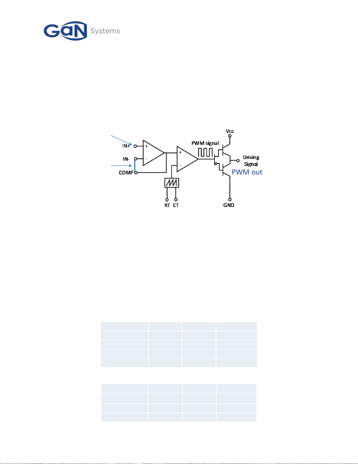
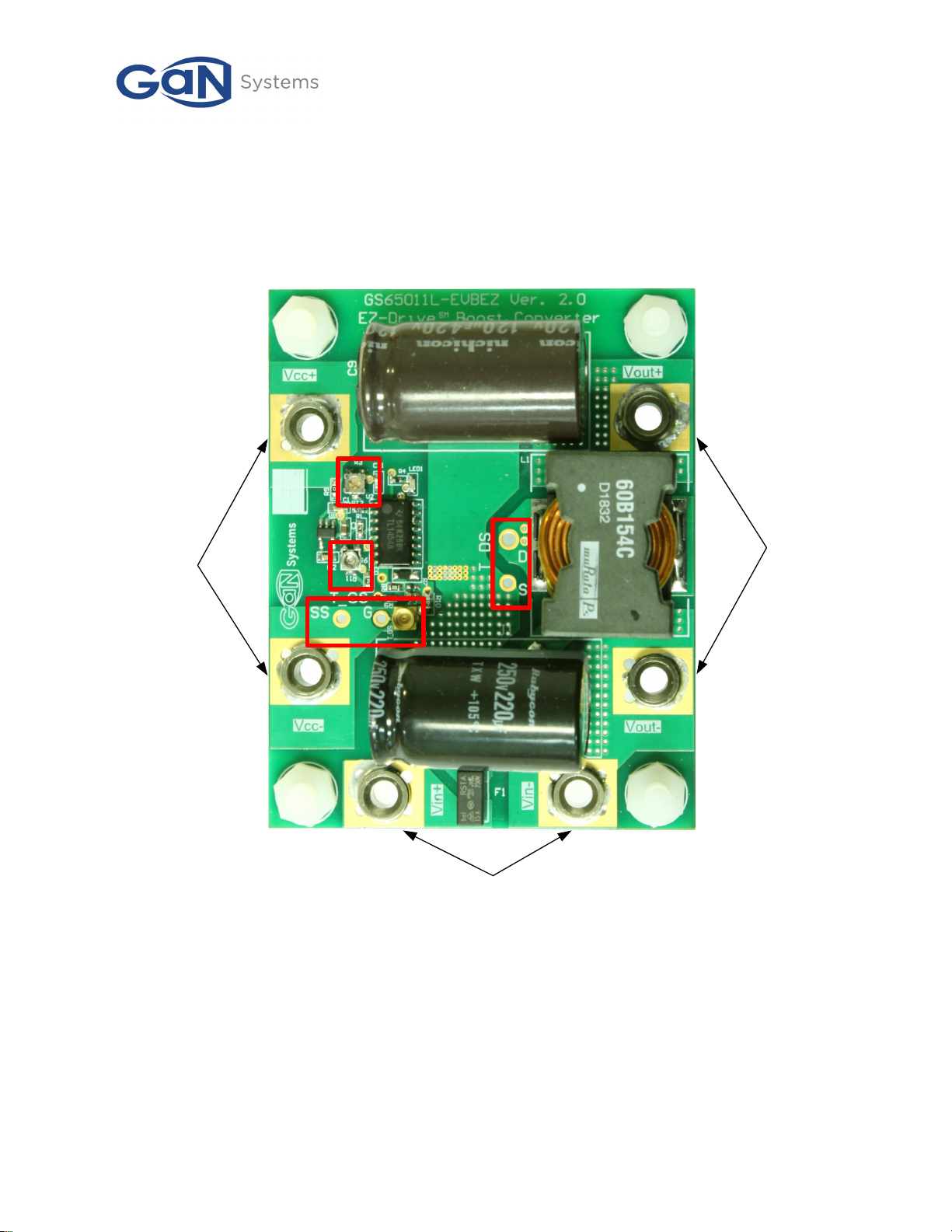
The GS65011-EVBEZ EVB is a GaN-based open-loop DC/DC Boost converter. It is
assembled with the EZDriveTM GaN driving circuit, a Si MOSFET PWM controller
(TL1454ACNSR) and a 650V 5×6 mm PDFN package GaN E-HEMT, (GS-065-011-1-L).
The PWM control signal is generated internally by the PWM controller, U2.
The EZDriveTM uses a Si MOSFET controller to drive a GaN HEMT which has a lower
threshold voltage. The EZDriveTM circuit is shown in the dotted box in Figure 2. It is a
low-cost, low component-count circuit composed of two Zener diodes, one capacitor,
three resistors and one diode.
ZDEZ1, ZDEZ2 clamp the positive and negative gate drive voltages. CEZ holds a negative
voltage for GaN E-HEMT turn-off. REZ sets the minimum driving current required to
keep the GaN E-HEMT fully turned on. RGcontrols the turn-on speed and ROFF controls
the turn-off speed.
The two operation modes for EZDriveTM are:
•Mode 1: Assuming the Vcc of the controller is 12V, controller output is ON, the
driving voltage on the GaN E-HEMT is clamped to 6V by Zener diode ZDEZ. The
rest of the Vcc, 6V, is stored across the capacitor CEZ.
•Mode 2: The voltage stored in the CEZ is applied to the gate reversely, so the GaN
can be turned off quickly.
Through this circuit, the Si MOSFET PWM controller’s output voltage is converted to the
proper voltage thresholds for driving GaN Systems’ E-HEMTs.