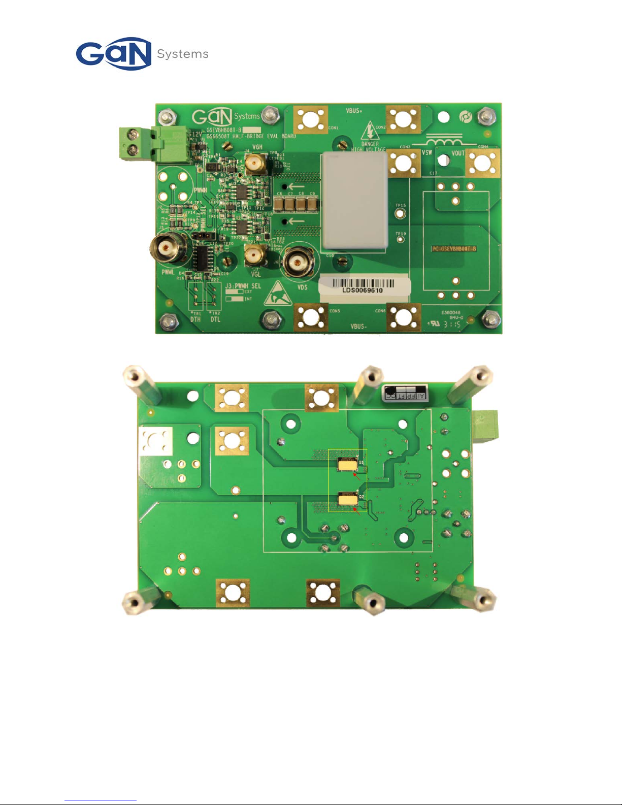
Gan Systems GS66508T-EVBHB User manual

GS66508T-EVBHB 650V
GaN E-HEMT Half Bridge Evaluation Board
User’s Guide
_____________________________________________________________________________________________________________________
GS66508T-EVBHB UG rev. 150917 © 2015 GaN Systems Inc. www.gansystems.com 1
Please refer to the Evaluation Board/Kit Important Notice on page 21
GS66508T-EVBHB 650V GaN E-HEMT Half
Bridge Evaluation Board
User’s Guide
Visit www.gansystems.com for the latest version of this user’s guide.
DANGER!
Electrical Shock Hazard -Hazardous high voltage may be present on the
board during the test and even brief contact during operation may result
in severe injury or death. Follow all locally approved safety procedures
when working around high voltage.
Never leave the board operating unattended. After it is de-energized,
always wait until all capacitors are discharged before touching the board.
This board should be handled by qualified personnel ONLY.
CAUTION:
This product contains parts that are susceptible to damage by electrostatic
discharge (ESD). Always follow ESD prevention procedures when
handling the product.

GS66508T-EVBHB 650V
GaN E-HEMT Half Bridge Evaluation Board
User’s Guide
_____________________________________________________________________________________________________________________
GS66508T-EVBHB UG rev. 150917 © 2015 GaN Systems Inc. www.gansystems.com 2
Please refer to the Evaluation Board/Kit Important Notice on page 21
Introduction
The GS66508T-EVBHB evaluation board (EVB) is designed to demonstrate the performance of GaN
Systems’ 650V GaN enhancement mode high electron mobility transistor (E-HEMT) devices. The EVB is a
fully functional half bridge power stage consisting of two 650V GaN E-HEMTs (top side cooled
GS66508T, 30A/55mΩ), gate drive power supply, half bridge gate drivers and heatsink. To evaluate the
performance of GaN E-HEMT devices in real power circuits, the EVB can be easily configured into any
half bridge based topology.The EVB and this USER’s Guide serve as a reference design for the gate
driver circuit, half bridge PCB layout and thermal management.
Functional Overview
Please refer to the circuit schematic in appendix for all signal names, circuit nodes and test points.
The block diagram of the GS66508T-EVBHB can be seen in Figure 1. All components are mounted on the
top side except for E-HEMTs, Q1 and Q2, which are mounted on the bottom side of the EVB. A heatsink
is mounted from the bottom side as well, in order provide cooling for the two GaN E-HEMTs. The board
includes all necessary components for building a half bridge power stage and provides footprints for
output power inductors and capacitors to allow users to configure the board into different operational
modes.
Figure 1 - GS66508T-EVBHB Evaluation Board Block Diagram
D
S
D
S
VSW
Q1
GS66508T
VBUS+
HS Gate
Driver
LS Gate
Driver
G
G
Q2
GS66508T
VBUS-
VOUT
VDS
VGL
VGH
External Mount Power
Inductor (not included)
Optional Output
Capacitor
9-12V
INPUT
Dead-time
generation
circuit
PWML
PWMH
N/I
TR1 TR2
Optional Deadtime
Adjustment Trimpot
N/I N/I
N/I – NOT INSTALLED
J3
J1
J2
J5
High side
PWM Select
N/I

GS66508T-EVBHB 650V
GaN E-HEMT Half Bridge Evaluation Board
User’s Guide
_____________________________________________________________________________________________________________________
GS66508T-EVBHB UG rev. 150917 © 2015 GaN Systems Inc. www.gansystems.com 3
Please refer to the Evaluation Board/Kit Important Notice on page 21
Figure 2 - Board overhead view
Figure 3 - Board bottom view –showing 2x GS66508T with heatsink removed

GS66508T-EVBHB 650V
GaN E-HEMT Half Bridge Evaluation Board
User’s Guide
_____________________________________________________________________________________________________________________
GS66508T-EVBHB UG rev. 150917 © 2015 GaN Systems Inc. www.gansystems.com 4
Please refer to the Evaluation Board/Kit Important Notice on page 21
Power input (J1)
Figure 4 - Power Input (J1)
The board can be powered by 9-12VDC on J1. The
supply voltage absolute maximum is 15V. On-board
voltage regulators create +5V for the logic circuit and
+6.5V for the gate driver.
Gate input (J2/J5)
Figure 5 - Gate signal input (J2/J5)
Set signal generator output level to 5V with 50Ω impedance for the gate PWM signal input on connector
J5. The high side gate drive signal can be configured by jumper J3. By default, J3 is set to the INT position
(internal, created by an on-board circuit). The on-board logic circuit inverts the PWM input on J5 to create
a complementary signal for the high side gate drive with dead time. To implement independent control
of the high side gate set J3 to EXT position (external, supplied by user on J2). Remove R13/R14 (R5/R6 for
J2) if high impedance input is required (e.g. from the logic output of a microcontroller).

GS66508T-EVBHB 650V
GaN E-HEMT Half Bridge Evaluation Board
User’s Guide
_____________________________________________________________________________________________________________________
GS66508T-EVBHB UG rev. 150917 © 2015 GaN Systems Inc. www.gansystems.com 5
Please refer to the Evaluation Board/Kit Important Notice on page 21
Dead time control
Figure 6 - Dead time control circuit
Dead time is controlled by two RC delay circuits, R16/C15 and R22/C19. By default, 100ns dead time is
used. Additionally two potentiometers locations are provided (TR1/TR2, not included) to allow fine
adjustment of the dead time if needed.

GS66508T-EVBHB 650V
GaN E-HEMT Half Bridge Evaluation Board
User’s Guide
_____________________________________________________________________________________________________________________
GS66508T-EVBHB UG rev. 150917 © 2015 GaN Systems Inc. www.gansystems.com 6
Please refer to the Evaluation Board/Kit Important Notice on page 21
Gate driver circuit
Figure 7 - Half bridge gate driver circuit
Gate drive power supply
A low side adjustable LDO (U5) steps down the input 9-12V to 6.5V for optimal gate drive. Bootstrap
diode (D1) and capacitor (C4) are used to create a floating gate drive power supply for the high side gate
drive circuit. The bootstrap voltage on C4 is then regulated by LDO (U2) to create a nominal 6.5V for
optimal gate drive.
Gate resistance
Turn-on gate resistors, R7/R18, are populated with 24.9Ωresistors. These resistors can be adjusted to
control the turn-on slew rate. Generally it is recommended to select turn-on gate resistance between 15-
25Ω for optimal performance. Smaller turn-on gate resistor values may create fast switching speeds
causing unnecessary Miller turn-on and oscillation. For turn-off it is recommended to use a small value
of less than 2Ωfor the turn-off gate resistors R10/R21. This will provide a strong pull-down during turn-
off and reduce the Miller voltage effects.
6.5V Gate Drive
VIN
600V 1A
P/N: ES1J
SMA
D1
0V
C4
1uF
0VGDH
R1
1R IN
GND
OUT
MIC5225YM5
VDRVH
0VGDH
ADJ
EN
R2
42K2
R3
10K
0VGDH
TP2
TP4
D
G
S
24R9
VDD
ANODE VO1
VO2
GND
R7
0R
R10
SI8261BAC
0VGDH
C5
2.2uF
CATH
N/C2
332R
N/C1
D2
0VGDH
FB1
15R@100MHz
0V
PMEG2010
0VGDH
U2
R8
TP8
GOH
R11
10K
TP7
VDDH
TP6
INH
TP11
HIGH SIDE FLOATING
GROUND
TP10
0VH TP12
0VGDH
J4
VGH
VSSH GNDH
U3
D
G
S
G
VIN
0V
C14
1uF
IN
GND
OUT
MIC5225YM5
VDRVL
0V
ADJ
EN
R15
42K2
R17
10K
24R9
VDD
ANODE VO1
VO2
GND
R18
0R
R21
SI8261BAC
0V
C16
2.2uF
CATH
N/C2
332R
N/C1
D3
0V
FB2
15R @100MHz
0V
PMEG2010
0V
U5
R19
TP18
GOL
R23
10K
TP17
VDDL
TP16
INL
TP21
TP20
0VL TP22
0V
J7
U6 VGL
VSSL GNDL
G
DZ4 (C18)
SOD323
6.8V 200mW
DZ3 (C11)
SOD323
6.8V 200mW

GS66508T-EVBHB 650V
GaN E-HEMT Half Bridge Evaluation Board
User’s Guide
_____________________________________________________________________________________________________________________
GS66508T-EVBHB UG rev. 150917 © 2015 GaN Systems Inc. www.gansystems.com 7
Please refer to the Evaluation Board/Kit Important Notice on page 21
Gate capacitor and clamping Clamping diode
An additional gate capacitor per drive circuit (C11/C18) is used to help shunt the Miller current and
reduce the Miller effect. The recommended value is between 100-220pF.
A clamping diode is placed close to thebetween the gate and source of each E-HEMT (DZ31/DZ42, on the
location of C11 and C18) for clamping negative gate voltage spikes induced by negative dv/dt on the
drain. It should be a fast Schottky diode or a zener diode (6.8V, 200mW, P/N: MMSZ5235BS-7-F). Added
Zener or schottky diode may contribute to gate oscillation combined with the parasitic inductance so it is
recommended to insert a ferrite bead in between clamping diode and the gate if to suppress any
unwanted gate oscillation is observed.
Ferrite bead
Ferrite bead on the gate helps to damp the gate ringing and reduce the risk of gate oscillation. On the
other hand adding ferrite bead increases the gate inductance and risk of miller turn-on. A small surface
mount device (SMD) EMI suppression ferrite bead with impedance of 10-20Ω @100MHz is sufficient for
suppressing gate oscillation while having minimal impact on the gate miller voltage. On this board a
ferrite bead is used on the gate for each devicehigh side only, FB1/FB2, (15Ω @100MHz, 0.5A, Wurth
Electronics P/N: 74279268) to stabilize the gate driver and suppress the gate ringing.
Testing your own gate driver
Figure 8 - Layout of testing pads for gate driver
Six square pads are provided around the gate driver as testing points as well as providing connection
pads for a user designed add-on gate driver board. The pads are on a 0.1” grid to allow users to
experiment with their own gate driver circuit. In this case the existing gate drive circuit(s) should be de-
populated from the EVB.
GATEVDD
IN+
VSSIN-
ISOLATION
VSS
0.3 [7.62]
0.2 [5.08]
0.3 [7.62]
Inch [mm]
GATE
INPUT GATE
OUTPUT

GS66508T-EVBHB 650V
GaN E-HEMT Half Bridge Evaluation Board
User’s Guide
_____________________________________________________________________________________________________________________
GS66508T-EVBHB UG rev. 150917 © 2015 GaN Systems Inc. www.gansystems.com 8
Please refer to the Evaluation Board/Kit Important Notice on page 21
Measurements
Drain voltage (VDS, J8)
Use a probe tip-to-BNC adapter and high voltage probe
for low side drain voltage VDS (switching node)
measurements. Avoid using a long ground lead for best
accuracy.
Gate drive signal (VGL, VGH)
The board includes two SMA connectors, J4 (high side
VGH) and J7 (low side VGL), for gate drive signal
measurements.
WARNING!
ALWAYS use high voltage differential or isolated probes for measuring high
side floating signals.
Attaching probe to high side gate signal may affect the switching behaviors
due to the added parasitic and coupling capacitance introduced by the
probe. To obtain best switching performance it is recommended to only
measure VGH for verifying gate driver operation at low voltage and remove
the probe during operation.
Measuring device temperature
Q1 and Q2 are located on the bottom side, as previously
indicated. Two PCB holes are aligned at the center of
package for measuring the device package temperature.
Use a thermal camera or attach thermocouples through
the two PCB holes for monitoring the device
temperature.

GS66508T-EVBHB 650V
GaN E-HEMT Half Bridge Evaluation Board
User’s Guide
_____________________________________________________________________________________________________________________
GS66508T-EVBHB UG rev. 150917 © 2015 GaN Systems Inc. www.gansystems.com 9
Please refer to the Evaluation Board/Kit Important Notice on page 21
Cooling
Figure 9 - Board thermal management
The board includes a customized heatsink attached to the PCB from the bottom side via 4 push pins. The
heatsink has a central pedestal copper block (20mmx20mm, 3mm height) that makes contact with the
thermal pads of two top side cooled GaN devices (GS66508T). A layer of thermal interface material (TIM,
Bergquist® Hi-Flow phase change 300P) is applied between heatsink and device thermal pad to provide
the required electrical insulation. Note that each thermal pad is connected to the substrate of the E-
HEMTs and is also internally electrically connected to the Source of the device.
Forced air cooling is recommended for power testing. The airflow direction should be controlled from
the left side as shown in Figure 9for best cooling performance.
CAUTION:
Device temperature must be closely monitored during the test. Never
operate the board with device temperature exceeding TJ_MAX (150°C)
Power Stage Setup
Power connections (CON1-6)
CON1-CON6 mounting pads are designed to be compatible with:
•#10-32 Screw mount,
•Banana Jack PCB mount (Keystone P/N: 575-4), or
•PC Mount Screw Terminal (Keystone P/N: 8191)
Output passives (L and C17)
An external power inductor (not included) can be connected between VSW (CON3) and VOUT (CON4)
or VBUS- (CON5/6), depending on the operation mode (see below). Users can choose their inductor size
to meet the test requirement. Generally it is recommended to use toroid power inductor with low inter-
winding capacitance to obtain best switching performance. For pulse testing we used 2x 60uH/40Amp
inductor (CWS, P/N: HF467-600M-40AV) in series.
GS66508T TIM
Heatsink central
block 20x20mm
Cross section view
FAN
Airflow direction

GS66508T-EVBHB 650V
GaN E-HEMT Half Bridge Evaluation Board
User’s Guide
_____________________________________________________________________________________________________________________
GS66508T-EVBHB UG rev. 150917 © 2015 GaN Systems Inc. www.gansystems.com 10
Please refer to the Evaluation Board/Kit Important Notice on page 21
C17 is designed to accommodate a film capacitor as output filter (not included). It has a universal
footprint that is compatible with Vishay MKP1848 series film capacitor 700V 1 to 35uF (P1=27.5-37.5mm,
P2=0-10.2mm, 2 or 4pins).
Operation mode
The board can be configured to any half bridge based topology and used as the building block for real
power conversion circuits. There are generally three operation modes:
Pulse test mode
Figure 10 - Pulse test mode and waveforms
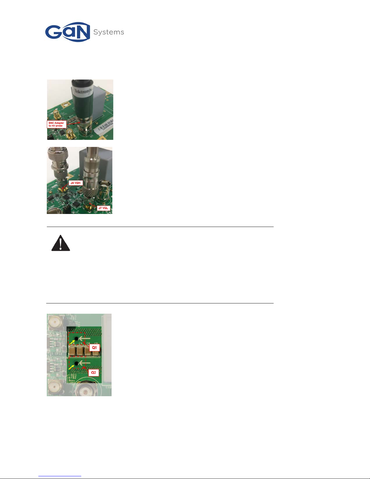
Similar to a standard double pulse testing circuit, the user can test half bridge inductive switching
performance by connecting the inductor from VSW to VBUS-. In this mode, the high side device Q1 is
hard switching (control) and low side Q2 is used as free-wheeling device (sync), which is driven
synchronously.
Figure 10 shows an example of the PWM input signal and pulse test switching waveforms for the pulse
test mode. Since a bootstrap circuit is used to create the high side gate voltage, the low side device Q2
must be turned on first before the first testing pulse to ensure that the high side gate driver is powered
up. This can be implemented by setting the signal generator output to “Inverse” mode on the signal so
the PWML is always high before and after the testing pulses. It is recommended to use a single trigger
burst mode and manually trigger the signal generator for each test to avoid any heating of the devices.
The maximum switching current for pulse test can be calculated by:
IL_MAX = TON * N * VDS / L, (Eq.1)
Where TON is the turn-on time per cycle, N is the total number of testing pulses and L is the inductance.
Set N = 3-5 to test the switching performance at different current ranges. Choose the inductance value
between 50 to 200uH and use the inductor with a current rating higher than your switching test current to
avoid saturation.
Trigger
+5V
0V
PWML
INPUT ...
N Cycles
VDS
IL
IL_MAX
T
ON
D
S
D
S
CON3
Q1
GS66508T
CON1
G
Q2
GS66508T
VBUS-
CON4
G
CON2
L
400V
+
VBUS+
CON6
CON5
VSW
IL
VDS
VGH

GS66508T-EVBHB 650V
GaN E-HEMT Half Bridge Evaluation Board
User’s Guide
_____________________________________________________________________________________________________________________
GS66508T-EVBHB UG rev. 150917 © 2015 GaN Systems Inc. www.gansystems.com 11
Please refer to the Evaluation Board/Kit Important Notice on page 21
CAUTION:
Limit the maximum switching current to 30A and ensure maximum
drain voltage including ringing is below 650V for pulse testing.
Exceeding this limit may cause damage to the devices.
Buck/Standard half bridge mode
This is standard half bridge configuration that can
be used in following circuits :
•Synchronous Buck DC/DC
•Single phase half bridge inverter
•ZVS LLC
•Phase leg for full bridge DC/DC or
•Phase leg for a 3-phase motor drive
Boost mode
When the output becomes the input and the load
is attached between VBUS+ and VBUS-, the board
is converted into a boost mode circuit and can be
used for:
•Synchronous Boost DC/DC
•Totem pole bridgeless PFC
Quick start procedure (pulse test mode)
1. Equipment and components you will need to get started:
•Four-channel oscilloscope with 500MHz bandwidth or higher
•high bandwidth (500MHz or higher) passive probe
•high bandwidth (500MHz) high voltage probe (>600V)
•AC/DC current probe for inductor current measurement
•12V DC power supply for board gate drive circuit
•Signal generator capable of creating testing pulses
•High voltage power supply (0-400VDC) with current limit.
•HV Differential probe for high side measurement (optional)
•External power inductor (recommend toroid inductor 50-200uH/40A)
1. Check the board for any visual damage and ensure jumper J3 is properly installed at “INT”
position.
D
S
D
S
CON3
Q1
GS66508T
CON1
G
Q2
GS66508T
VBUS-
CON4
G
C6-C10
CON2
L
OUT
400V DC
+
VBUS+
CON6
CON5
VSW
C
OUT
D
S
D
S
CON3
Q1
GS66508T
CON1
G
Q2
GS66508T
VBUS-
CON4
G
C6-C10
CON2
L
IN
+
VBUS+
CON6CON5
VSW VIN
INPUT

GS66508T-EVBHB 650V
GaN E-HEMT Half Bridge Evaluation Board
User’s Guide
_____________________________________________________________________________________________________________________
GS66508T-EVBHB UG rev. 150917 © 2015 GaN Systems Inc. www.gansystems.com 12
Please refer to the Evaluation Board/Kit Important Notice on page 21
2. Connect 12VDC power supply to J1 (positive on the top). Turn on the output and ensure that
standby current is below 20mA. (Typical 10-15mA).
3. Connect 50Ωimpedance output from signal generator to J5 (PWML). Set up the signal generator
in pulse and single trigger burst mode to generate signals as shown in Figure 10. Set Ncycle = 5
and use the Eq.1 to calculate TON to ensure the maximum switching current is ≤30A at 400VDC.
4. Trigger the signal generator and confirm that gate drive signals VGL and VGH are present and
the gate voltage levels are correct.
5. Connect the probes as shown in Figure 11, for the following measurements:
a. VGL (J7): low side gate signal, passive probe
b. VDS (J6): low side drain voltage, HV probe
c. VGH (J4): high side gate signal, HV differential probe (optional)
d. IL: current probe for inductor current
6. Set the High Voltage (HV) DC supply voltage level to 0V and ensure that the output is OFF.
Connect the HV supply output to CON1 (VBUS+) and CON5 (VBUS-). Attach the external
inductor between CON3 (VSW) and CON6 (VBUS-).
7. Set the oscilloscope to single trigger mode. Turn on the output of the HV supply and slowly ramp
the voltage up. Then trigger the signal generator and observe the voltage and current waveforms.
8. After the test is complete, slowly ramp down the HV supply voltage to 0V and turn off the
output. Then turn off the 12V power supply and signal generator output.
Figure 11 - Example of pulse Test set up
The picture can't be displayed.

GS66508T-EVBHB 650V
GaN E-HEMT Half Bridge Evaluation Board
User’s Guide
_____________________________________________________________________________________________________________________
GS66508T-EVBHB UG rev. 150917 © 2015 GaN Systems Inc. www.gansystems.com 13
Please refer to the Evaluation Board/Kit Important Notice on page 21
Test results
Pulse test (VDS=400V, IMAX = 30A, TON=2us, N=5, L=120uH)
Pulse test results show that the gate driver is stable for the entire operating range from 0-30A with no
oscillation and minimum drain voltage overshoot.
Figure 12 - Pulse Test waveforms (400V/30A)
The measured rise time for turn-on is 10ns and the fall time at 30A turn-off is 6ns. The miller voltage is
under good control with a peak value of 0.8V which is lower than gate threshold of 1.6V at a dv/dt =
40V/ns and the turn-off negative voltage is clamped by the diode with a peak negative spike of
approximately -2V.

GS66508T-EVBHB 650V
GaN E-HEMT Half Bridge Evaluation Board
User’s Guide
_____________________________________________________________________________________________________________________
GS66508T-EVBHB UG rev. 150917 © 2015 GaN Systems Inc. www.gansystems.com 14
Please refer to the Evaluation Board/Kit Important Notice on page 21
a) Turn-on waveforms (400V/22A) b) Turn-off waveforms (400V/30A)
Figure 13 - Pulse test switching waveforms turn-on and turn-off
Synchronous Buck Test (L=120uH, VIN=400V, VOUT=200V, D=50%, FSW=100 kHz, POUT =0-2kW)
The board is converted to a synchronous buck DC/DC converter and demonstrates efficiency >98.5% from
1kW to 2kW. With forced air cooling, the peak device temperature TJ_MAX was measured at <80°C at
1500W output.
Figure 14 - Synchronous Buck Efficiency (VIN=400V, VOUT=200V, D=50%, FSW=100kHz)

GS66508T-EVBHB 650V
GaN E-HEMT Half Bridge Evaluation Board
User’s Guide
_____________________________________________________________________________________________________________________
GS66508T-EVBHB UG rev. 150917 © 2015 GaN Systems Inc. www.gansystems.com 15
Please refer to the Evaluation Board/Kit Important Notice on page 21
Figure 15 - Synchronous Buck switching waveforms (CCM, POUT=1500W)
Figure 16 - Thermal image showing Q1 and Q2 temperature (POUT=1500W, TJMAX=80°C, TAMB=25°C)

GS66508T-EVBHB 650V
GaN E-HEMT Half Bridge Evaluation Board
User’s Guide
_____________________________________________________________________________________________________________________
GS66508T-EVBHB UG rev. 150917 © 2015 GaN Systems Inc. www.gansystems.com 16
Please refer to the Evaluation Board/Kit Important Notice on page 21
Appendix
Schematic
6.5V Gate Drive
VIN
600V 1A
P/N: ES1J
SMA
D1
C3
1uF
0V
C4
1uF
0VGDH
R1
1R IN
GND
OUT
MIC5225YM5
VDRVH
0VGDH
J1
C1
10uF
0805
9-12V
INPUT
VIN
IN
GND
OUT
LP2980
N/C
INHB
0V
+5V
C2
10uF
0805
TP1
TP3
ADJ
EN
R2
42K2
R3
10K
0VGDH
TP2
TP4
D
G
S
GS66508T
24R9
VDD
ANODE VO1
VO2
GND
R7
0R
R10
SI8261BAC
Q1
0VGDH
C5
2.2uF
CATH
N/C2
332R
N/C1
D2
0VGDH
FB1
15R@100MHz
0V
PMEG2010
0VGDH
U2
R8
6.8V 200mW
SOD323
TP8
GOH
R11
10K
GANPX-T
G
TP7
VDDH
TP6
INH
TP11
HIGH SIDE FLOATING
GROUND
TP10
0VH TP12
VBUS+ CON2
C6
0.1uF 1kV
1812
C7
0.1uF 1kV
1812
C8
0.1uF 1kV
1812
C9
0.1uF 1kV
1812
C10
10uF 700V
MKP1848
0V
D
G
S
GS66508T
Q2
GANPX-T
G
CON1
CON3
VSW
VIN
0V
C14
1uF
IN
GND
OUT
MIC5225YM5
VDRVL
0V
ADJ
EN
R15
42K2
R17
10K
24R9
VDD
ANODE VO1
VO2
GND
R18
0R
R21
SI8261BAC
0V
C16
2.2uF
CATH
N/C2
332R
N/C1
D3
0V
FB2
15R@100MHz
DZ4 (C18)
0V
PMEG2010
0V
U5
R19
SOD323
TP18
GOL
R23
10K
TP17
VDDL
TP16
INL
TP21
TP20
0VL TP22
0VGDH
J4
0V
J7
VOUT
VGH
WARNING!
USE HV DIFFERENTIAL
PROBES ON HIGH SIDE
SIGNALS
VSSH GNDH
U3
U4C
U4B
J3
U4A D4
PMEG2010
R16
1K
TR1
2K
0V
C15
100pF
+5V
0V
OPT
DTH
C12
0.22uF
C13
1uF
0V
PWM_H SELECT 1
1-2 EXTERNAL
2-3 INTERNAL
PMEG2010
R22
1K
TR2
2K
0V
C19
100pF
OPT
DTL
U4D
D5
HIGH SIDE PWM
GENERATOR
U6
HS DEAD TIME
ADJ
LS DEAD TIME
ADJ
VGL
74VHC132 74VHC132
74VHC132
R12
100R
0V
J5
PWML
R13
R14
100R
100R
1206
1206
R4
100R
J2
R5
R6
100R
100R
1206
1206
PWMH EXT
OPT
J6
VDS
0V
TP15
TP16
TP5
TP9
TP13
TP14
C17
MKP1848 UNIV
CON4
CON5
VBUS-
CON6
OPTIONAL OUTPUT
CAPACITOR
UNIV. FOOTPRINT
FOR VISHAY MKP1848
700V/1-35uF
OPT
EXTERNAL MOUNT POWER INDUCTOR
NOTES – UNLESS OTHERWISE SPECIFIED
1. ALL SMD RESISTORS AND CAPACITORS ARE 0603 SIZE
2. DZ3 AND DZ4 INSTALLED ON LOCATION OF C11 AND C18.
VSSL GNDL
0V
6.8V 200mW
DZ3 (C11)

GS66508T-EVBHB 650V
GaN E-HEMT Half Bridge Evaluation Board
User’s Guide
_____________________________________________________________________________________________________________________
GS66508T-EVBHB UG rev. 150917 © 2015 GaN Systems Inc. www.gansystems.com 17
Please refer to the Evaluation Board/Kit Important Notice on page 21
PCB Layout
Top layer

GS66508T-EVBHB 650V
GaN E-HEMT Half Bridge Evaluation Board
User’s Guide
_____________________________________________________________________________________________________________________
GS66508T-EVBHB UG rev. 150917 © 2015 GaN Systems Inc. www.gansystems.com 18
Please refer to the Evaluation Board/Kit Important Notice on page 21
Bottom Layer

GS66508T-EVBHB 650V
GaN E-HEMT Half Bridge Evaluation Board
User’s Guide
_____________________________________________________________________________________________________________________
GS66508T-EVBHB UG rev. 150917 © 2015 GaN Systems Inc. www.gansystems.com 19
Please refer to the Evaluation Board/Kit Important Notice on page 21
Assembly Drawing (Top)

GS66508T-EVBHB 650V
GaN E-HEMT Half Bridge Evaluation Board
User’s Guide
_____________________________________________________________________________________________________________________
GS66508T-EVBHB UG rev. 150917 © 2015 GaN Systems Inc. www.gansystems.com 20
Please refer to the Evaluation Board/Kit Important Notice on page 21
Bill of materials
REFERENCE
QUANTITY
DESCRIPTION
MANUFACTURER
MANUFACTURER PN
NOTE
C1,C2
2
CAP CER 10UF 25V 10% X5R 0805
MURATA
GRM21BR61E106KA73L
C3,C4,C13,C14
4
CAP CER 1UF 25V 10% X7R 0603
TAIYO YUDEN
TMK107B7105KA-T
C5,C16
2
CAP CER 2.2UF 25V 10% X7R 0603
TAIYO YUDEN
LMK107B7225KA-T
C6,C7,C8,C9
4
CAP CER 0.1UF 1KV 10% X7R 1812
KEMET
C1812C104KDRAC7800
C10
1
Alternate
CAP FILM 10UF 700V P=27.5MM
CAP FILM 10UF 5% 600VDC RADIAL
VISHAY
KEMET
MKP1848610704K2
C4AEHBU5100A11J
C11,C18
2
CAP CER 220pF 25V 5% NP0 0603
KEMET
C0603C221J3GACTU
C12
1
CAP CER 0.22UF 25V 10% X7R 0603
TAIYO YUDEN
TMK107B7224KA-T
C15,C19
2
CAP CER 100PF 25V 5% NP0 0603
KEMET
C0603C101J3GACTU
C17
1
CAP FILM 10UF 700V
Vishay
MKP1848610704K2
DNP
DZ1,DZ2
2
DIODE ZENER 6.8V 200MW SOD323
DIODES INC
MMSZ5235BS-7-F
DNP
DZ3, DZ4 (C11,
C18)
2
DIODE ZENER 6.8V 200MW SOD323
DIODES INC
MMSZ5235BS-7-F
D1
1
DIODE GEN PURP 600V 1A SMA
FAIRCHILD
ES1J
D2,D3,D4,D5
4
DIODE SCHOTTKY 20V 1A 2DFN
NXP
PMEG2010EPK
FB1, FB2
12
FERRITE BEAD SMD 15 OHM 0.5A 0603
WURTH ELECTRONICS
74279268
FB2,R10,R21
32
RES SMD 0.0 OHM JUMPER 1/10W
VISHAY DALE
CRCW06030000Z0EA
J1
1
TERM BLOCK HDR 2POS R/A 5.08MM
TE CONNECTIVITY
796638-2
J2,J5,J6
3
CONN BNC JAC STR 50 OHM
AMPHENOL
112538
DNP J2
J3
1
CONN HEADER 3POS 2.54MM
WURTH ELECTRONICS
61300311121
J4,J7
2
CONN SMA JACK SMD VERT 50OHM
LINX
CONSMA001-SMD-G
Q1,Q2
2
TRANS GAN E-HEMT 650V 30A
GAN SYSTEMS INC
GS66508T-E01
R1
1
RES SMD 1.0 OHM 1% 1/8W 0805
VISHAY DALE
CRCW08051R00FKEA
R2,R15
2
RES SMD 42.2K OHM 1% 1/10W 0603
VISHAY DALE
CRCW060342K2FKEA
R3,R11,R17,R23
4
RES SMD 10K OHM 1% 1/10W 0603
VISHAY DALE
CRCW060310K0FKEA
R4,R12
2
RES SMD 100 OHM 1% 1/10W 0603
VISHAY DALE
CRCW0603100RFKEA
R5,R6,R13,R14
4
RES SMD 100 OHM 1% 1/4W 1206
VISHAY DALE
CRCW1206100RFKEA
R7,R18
2
RES SMD 24.9 OHM 1% 1/10W 0603
VISHAY DALE
CRCW060324R9FKEA
R8,R19
2
RES SMD 332 OHM 1% 1/10W 0603
VISHAY DALE
CRCW0603332RFKEA
R16,R22
2
RES SMD 1K OHM 1% 1/10W 0603
VISHAY DALE
CRCW06031K00FKEA
TR1,TR2
2
RES TRIMMER 2K OHM 1/2W TH
MURATA
PV36W202C01B00
DNP
U1
1
IC REG LDO 5V 50MA SOT-23-5
ST MICRO
LD2980ABM50TR
U2,U5
2
IC REG LDO ADJ 0.15A SOT23-5
MICREL
MIC5225YM5 TR
U3,U6
2
IC ISO GATE DRVR 4A 3.75KV
SILAB
SI8261BAC-C-IS
U4
1
IC GATE NAND 4CH 2-INP 14-SOIC
FAIRCHILD
74VHC132M
OFF THE BOARD COMPONENTS
J1-PLUG
1
TERM BLK PLUG
TE CONNECTIVITY
796634-2
J3-SHUNT
1
JUMPER SHUNT
TE CONNECTIVITY
382811-8
STANDOFF
6
HEX STDOFF 6-32 ALUM 1-1/4
KEYSTONE
8420
HEX NUTS
6
HEX NUT STEEL 6-32
KEYSTONE
4701
HEATSINK
1
heatsink, push pin Customized design
MALICO INC
CMFA0660502900-00
DNP = Do not populate
Table of contents
Other Gan Systems Motherboard manuals

Gan Systems
Gan Systems GS-EVB-HBDB-IMS User manual

Gan Systems
Gan Systems GS61004B-EVBCD User manual

Gan Systems
Gan Systems GSWP050W-EVBPA User manual

Gan Systems
Gan Systems GSP665HPMB-EVBIMS2 User manual

Gan Systems
Gan Systems GS66504B-EVBDB GaN E-HEMT User manual

Gan Systems
Gan Systems GSWP300W-EVBPA User manual

Gan Systems
Gan Systems GS65011-EVBEZ User manual

Gan Systems
Gan Systems GS66502B-EVBDB User manual

Gan Systems
Gan Systems GS-EVB-DRG-100V7R-GS2 User manual

Gan Systems
Gan Systems GSWP100W-EVBPA User manual