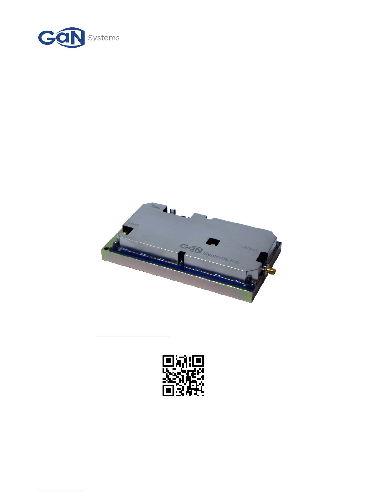
GSWP100W-EVBPA
GaN E-HEMT Wireless Power Transfer Evaluation Board
User’s Guide
_____________________________________________________________________________________________________________________
GSWP100W-EVBPA Rev 180529 © 2018 GaN Systems Inc. www.gansystems.com 9
Please refer to the Evaluation Board/Kit Important Notice on page 26
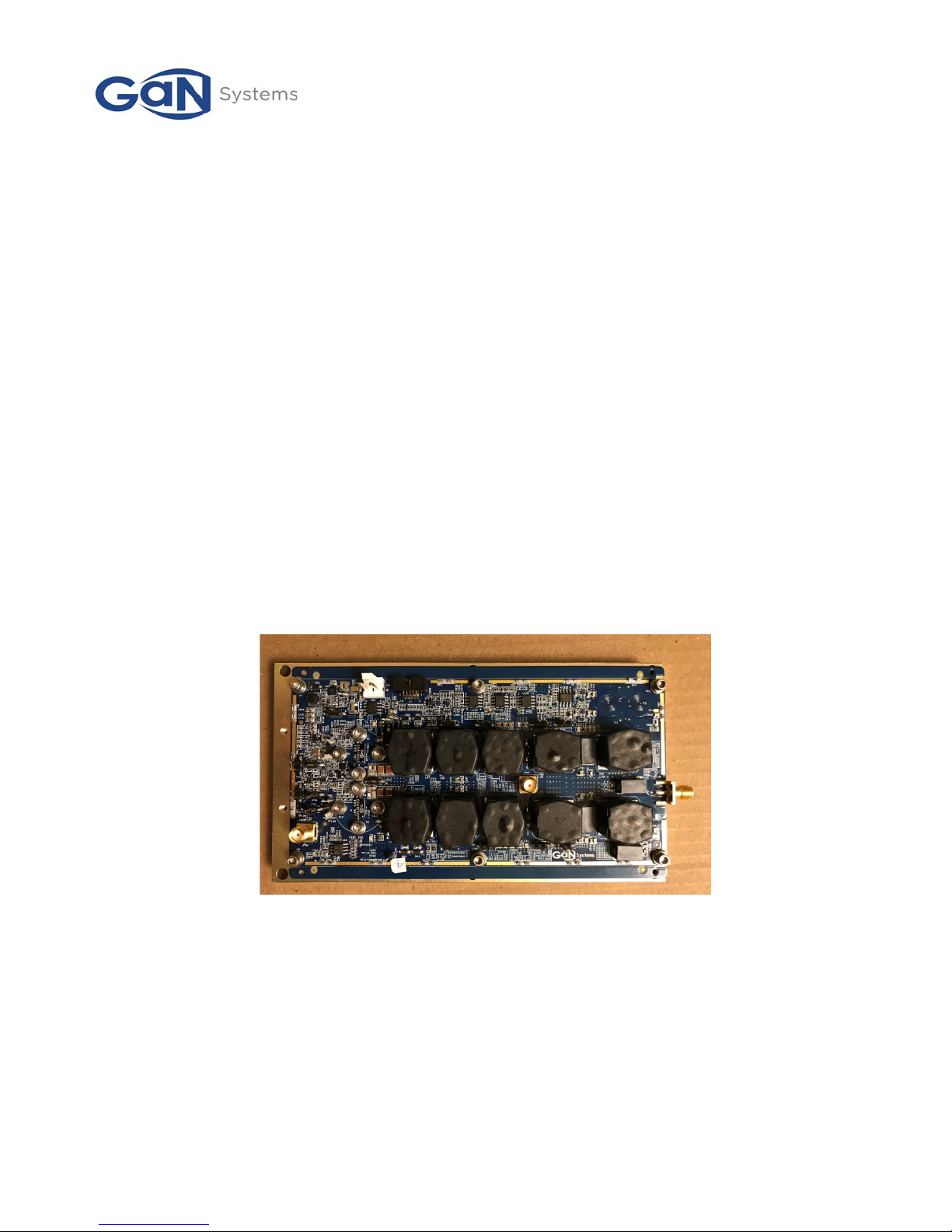
Circuit Description
The Push-Pull circuit is comprised of two single ended PAs which share a common supply, however;
the impedance matching and EMI filters are separated.
The high-side E-HEMTs are powered by a DC source, referred to as the HV supply. It is connected
through J32. The voltage of this source not exceed 33VDC.
The low-voltage logic circuitry runs off a 3.3VDC voltage regulator, U88, which is powered from a
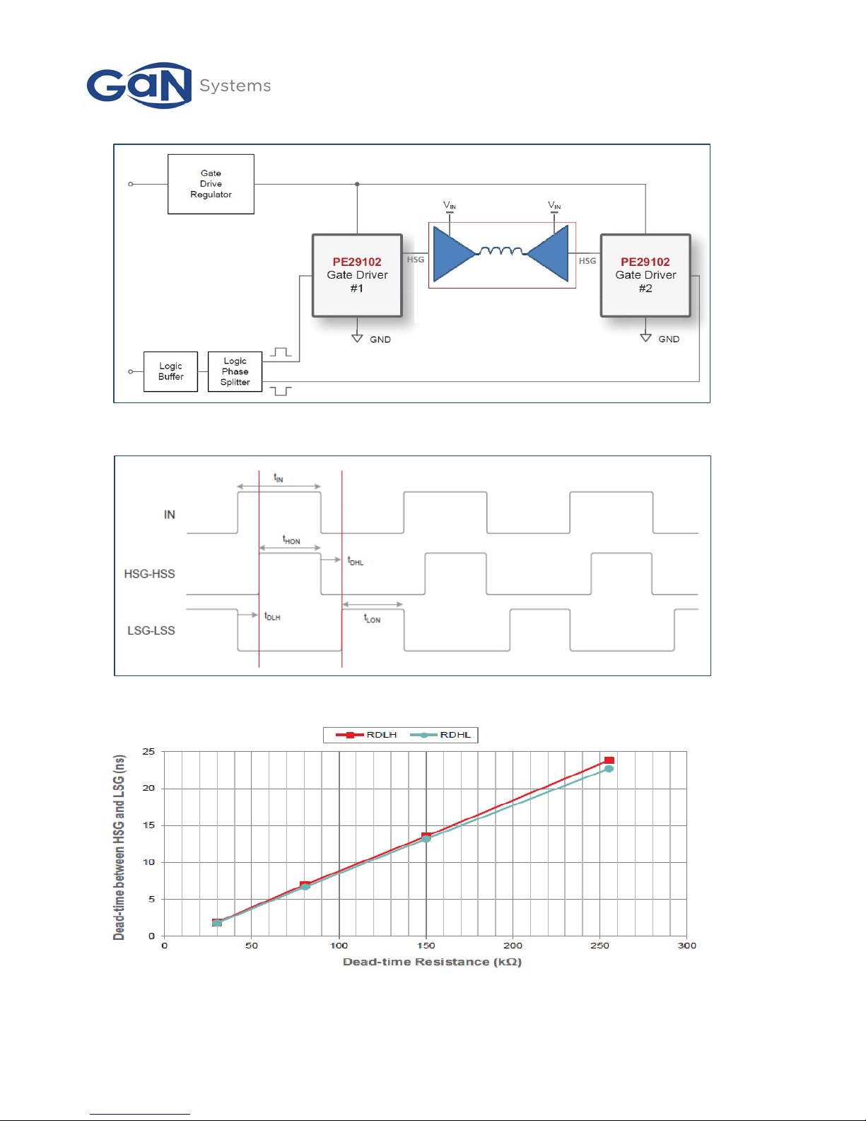
+5VDC source connected through JP35. The +5VDC rail also feeds two PE29102 drivers U86 and U90,
which are driven independently by U87, a common logic D-type flip/flop. U87 has a frequency
divider configuration, which is driven by a crystal oscillator Y8 at a frequency of 13.56MHz. The
two PE29102 gate drives are capable of 6V operation.
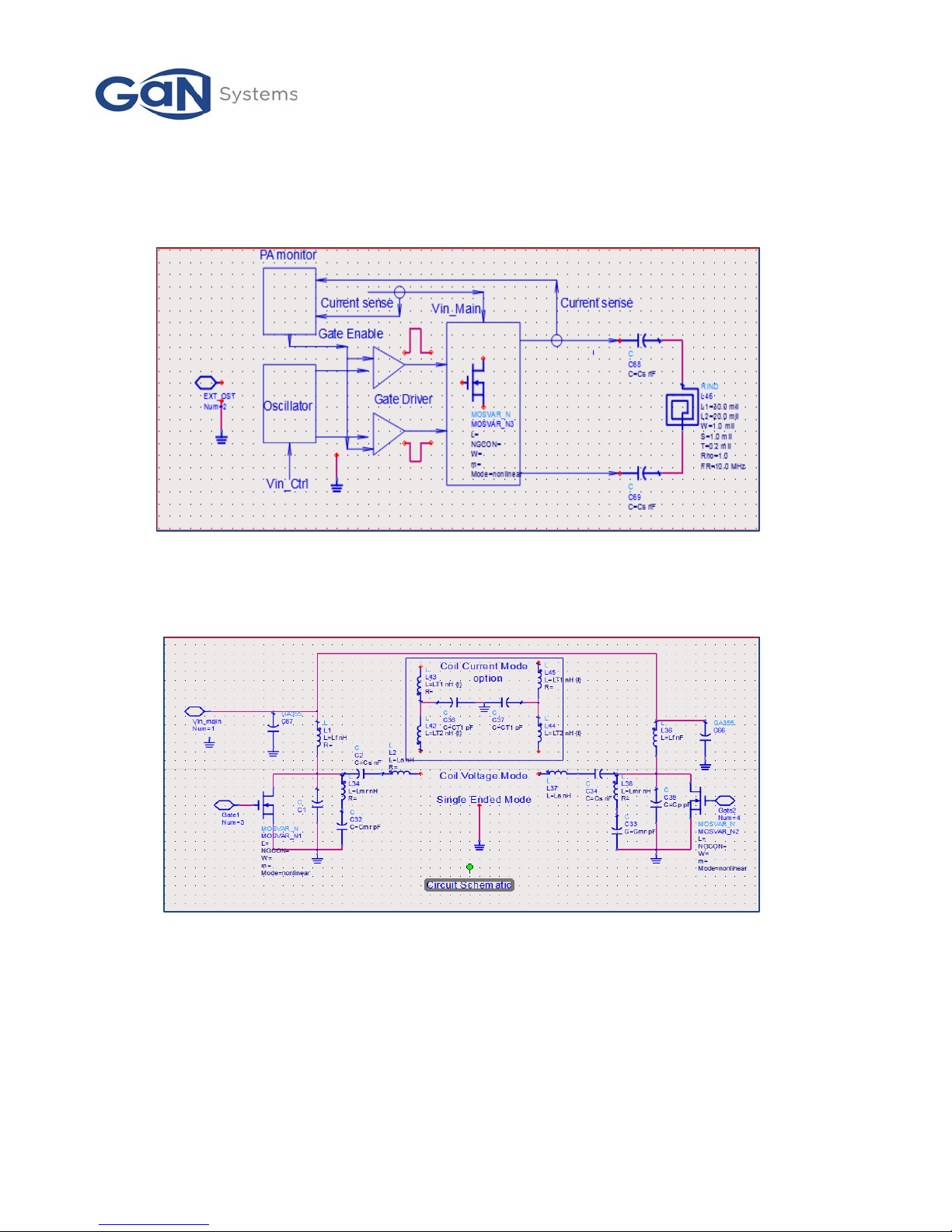
The PA can be configured to operate in a number of different modes, which include
•Push-pull configuration with an EMI filter
•Single ended mode
•Operation without an EMI filter
•Operation with an external oscillator signal input. Users can run multiple PAs together at
the same frequency for high power operation.
Detailed operation procedures and setup for these alternative configurations are provided in the
section titled “quick start guide”.
The PA includes an over-temperature protection circuit. Temperature sensor U9, placed close to the
GS61008P E-HEMTs, monitors their temperature. In an over-temperature condition, the PE29102A
driver will be disabled through U133 and stop driving the E-HEMTs. The design also includes
circuitry to protect against over-current, and load mismatch.
The evaluation board includes an EMI filter, comprised of one low pass filter and one notch filter.
The output of PA can be configured, through jumpers, to operate either with or without an EMI
filter. The detailed jumper and SMA connector configurations are listed in Table 4
For convenience, test points are provided to monitor and measure the electrical signals. A
description of the test points and diagram of their location is provided in Table 5.
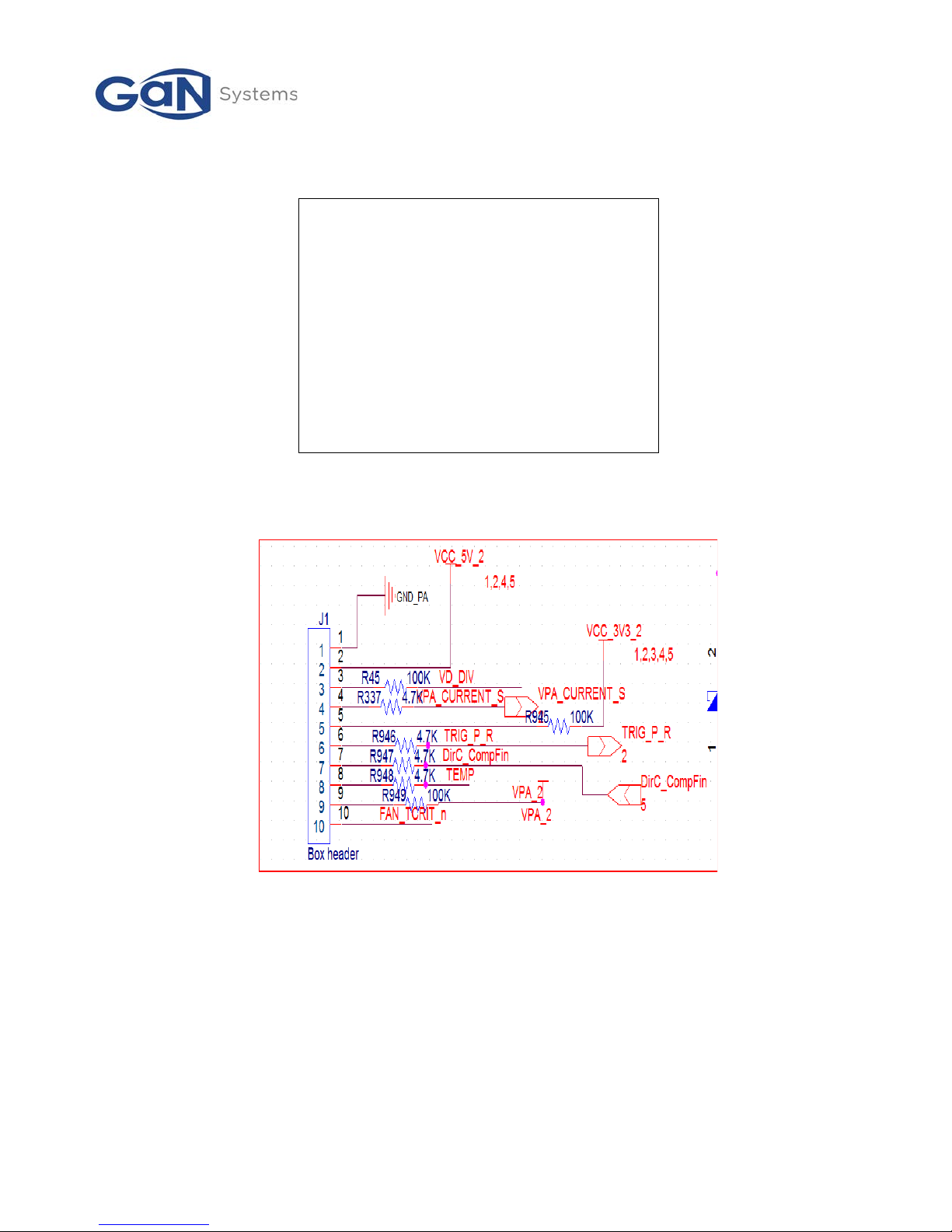
The PA also includes a Micro Controller Unit (MCU) monitor interface header, J1. The signals
available through J1 can be used to control the PA system for close loop in the WPT system. A
definition of the signals available on header J1 is provided in Figure 10.