Gan Systems GS61004B-EVBCD User manual

GS61004B-EVBCD
GaN E-HEMT Full Bridge Evaluation Board
User’s Guide
_____________________________________________________________________________________________________________________
GS61004B-EVBCD Rev 200106 © 2020 GaN Systems Inc. www.gansystems.com 1
Please refer to the Evaluation Board/Kit Important Notice on page 27
GS61004B-EVBCD
100V GaN E-HEMT Full Bridge Evaluation
Board.
User’s Guide
Visit www.gansystems.com for the latest version of this user’s guide.

GS61004B-EVBCD
GaN E-HEMT Full Bridge Evaluation Board
User’s Guide
_____________________________________________________________________________________________________________________
GS61004B-EVBCD Rev 200106 © 2020 GaN Systems Inc. www.gansystems.com 2
Please refer to the Evaluation Board/Kit Important Notice on page 27
DANGER!
Electrical Shock Hazard - Hazardous high voltage may be present on the board
during the test and even brief contact during operation may result in severe injury
or death. Follow all locally approved safety procedures when working around
high voltage.
Never leave the board operating unattended. After it is de-energized, always wait
until all capacitors are discharged before touching the board.
This board should be handled by qualified personnel ONLY.
PCB surface can become hot. Contact may cause burns. Do not touch!
CAUTION:
This product contains parts that are susceptible to damage by electrostatic
discharge (ESD) or exposure to voltages in excess of the specified voltage. Always
follow ESD prevention procedures when handling the product. Avoid applying
excessive voltages to the power supply terminals or signal inputs or outputs

GS61004B-EVBCD
GaN E-HEMT Full Bridge Evaluation Board
User’s Guide
_____________________________________________________________________________________________________________________
GS61004B-EVBCD Rev 200106 © 2020 GaN Systems Inc. www.gansystems.com 3
Please refer to the Evaluation Board/Kit Important Notice on page 27
Introduction
The GS61004B-EVBCD evaluation board allows the user to evaluate our GaN Systems’
GS61004B Enhancement mode-High Electron Mobility Transistors (E-HEMTs) with the
Peregrine PE29102 gate driver in a full-bridge configuration. The PE29102 integrated high-
speed driver is designated to control the gates of our E-HEMTs. The outputs of the PE29102 are
capable of providing switching transition speeds in the sub nano-second range for hard
switching applications.
This user’s guide includes the evaluation board schematic, circuit description, a quick-start
guide and measurement results.
Evaluation Kit Contents and Requirements
Kit Contents
The GS61004B-EVBCD EVB includes the following hardware required to evaluate the GaN E-
HEMT Driver.
Table 1 GS61004B-EVBCD Evaluation Kit Contents
Quantity Description
1
GaN E-HEMT Driver GS61004B Full-Bridge evaluation board assembly
Hardware Requirements
In order to evaluate the performance of the evaluation board, the following equipment is required:
•
DVM and/or oscilloscope
•
Function generator (PWM)
•
High voltage DC power supply
•
DC power supply
•
DC test leads
•
Loudspeaker or resistive load
•
3-way Molex KK type mating connector, crimp and cable for P1 (Mouser parts: 538-79758-0015,
538-10-11-2033)

GS61004B-EVBCD
GaN E-HEMT Full Bridge Evaluation Board
User’s Guide
_____________________________________________________________________________________________________________________
GS61004B-EVBCD Rev 200106 © 2020 GaN Systems Inc. www.gansystems.com 4
Please refer to the Evaluation Board/Kit Important Notice on page 27
Evaluation Board Assembly Overview
The evaluation board (EVB) is assembled with two PE29102 GaN E-HEMT drivers and four
GS61004B E-HEMT transistors. Headers are included for signal input, signal output, and power
connections. Probe points are included for waveform measurements. Provision has been made for
a single, suitable heatsink to be fastened against the four E-HEMTs, using the three holes in the
center of the board.
Figure 1 • GS61004B-EVBCD Evaluation Board Assembly

GS61004B-EVBCD
GaN E-HEMT Full Bridge Evaluation Board
User’s Guide
_____________________________________________________________________________________________________________________
GS61004B-EVBCD Rev 200106 © 2020 GaN Systems Inc. www.gansystems.com 5
Please refer to the Evaluation Board/Kit Important Notice on page 27
Block Diagram and Schematic
The block diagram and schematic of the evaluation board are provided in Figures 2, 3, and 4,
Figure 2 • PE29102 Full-Bridge EVB Block Diagram

GS61004B-EVBCD
GaN E-HEMT Full Bridge Evaluation Board
User’s Guide
_____________________________________________________________________________________________________________________
GS61004B-EVBCD Rev 200106 © 2020 GaN Systems Inc. www.gansystems.com 6
Please refer to the Evaluation Board/Kit Important Notice on page 27
Figure 3 • PE29102 Full-Bridge EVB Schematic (1 of 2)
Note: * CAUTION: Parts and assemblies susceptible to damage by electrostatic discharge (ESD).

GS61004B-EVBCD
GaN E-HEMT Full Bridge Evaluation Board
User’s Guide
_____________________________________________________________________________________________________________________
GS61004B-EVBCD Rev 200106 © 2020 GaN Systems Inc. www.gansystems.com 7
Please refer to the Evaluation Board/Kit Important Notice on page 27
Figure 4 • PE29102 Full-Bridge EVB Schematic (2 of 2)
Note: * CAUTION: Parts and assemblies susceptible to damage by electrostatic discharge (ESD).

GS61004B-EVBCD
GaN E-HEMT Full Bridge Evaluation Board
User’s Guide
_____________________________________________________________________________________________________________________
GS61004B-EVBCD Rev 200106 © 2020 GaN Systems Inc. www.gansystems.com 8
Please refer to the Evaluation Board/Kit Important Notice on page 27
Circuit Description
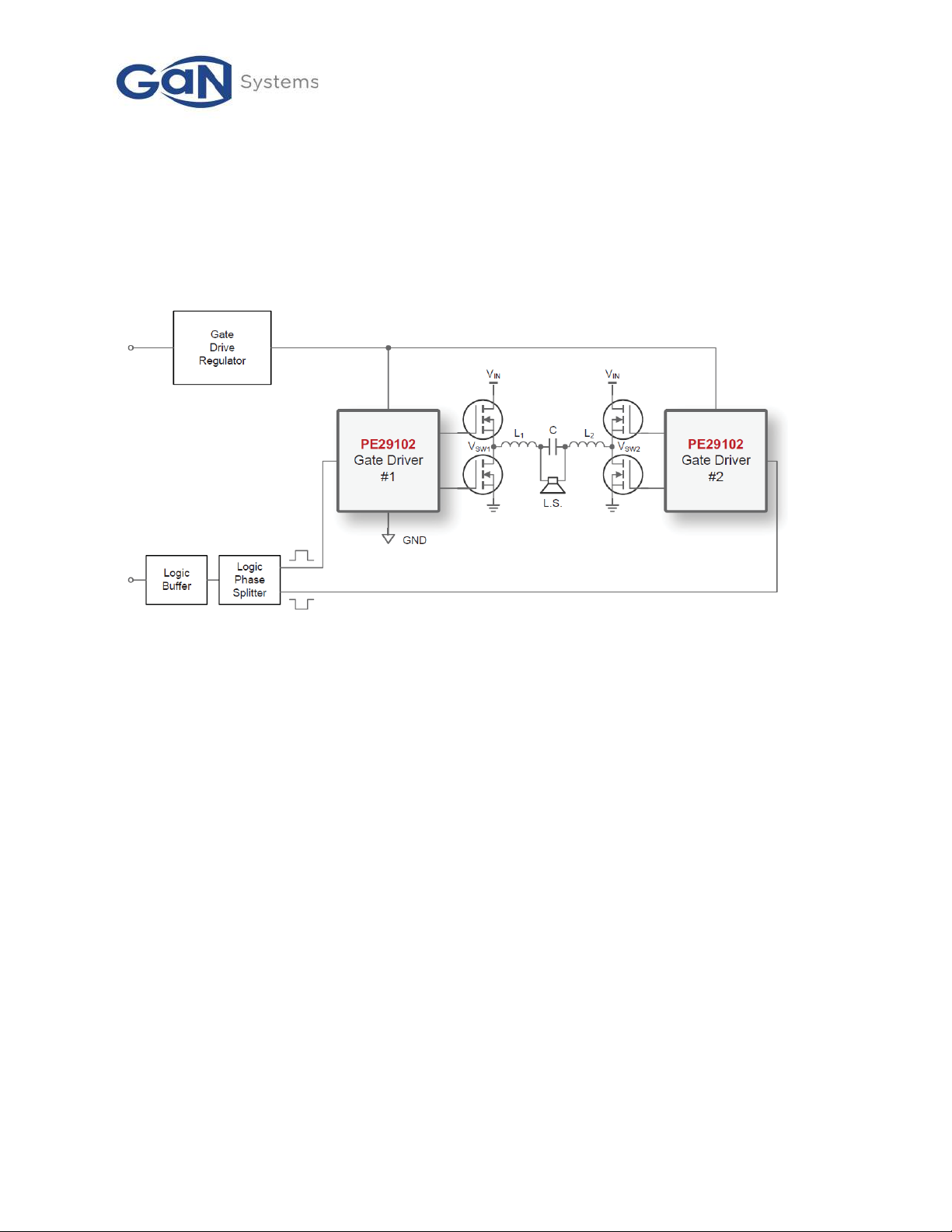
The full-bridge circuit comprises two half bridges which share a common supply and load.
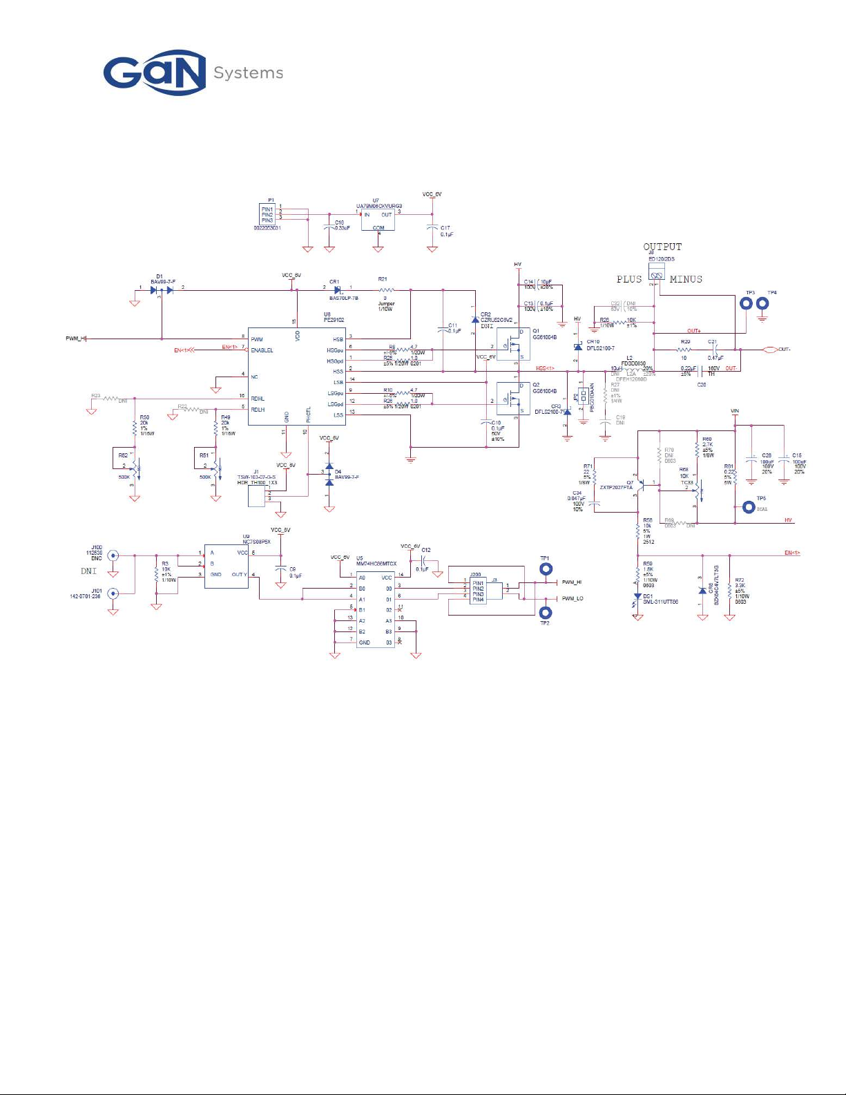
The high voltage (+12 to 30V DC max) to the high-side GS61004B E-HEMTs are fed via J7 and then
through the overcurrent protection circuit around Q7, which is described separately. The low-level
logic circuitry is supplied by a 6 Volt regulator U7, which is fed separately through P1 with +8 to
+24V DC (nominal +12V DC). This feeds the optimal 6V to both of the PE29102 drivers U6 and U8,
which are driven independently by a common logic X-OR gate Phase Splitter (Inverter)
configuration U5, which is in turn driven by a single input buffer, U9. The latter two devices are
also capable of 6V operation.
Typically, the PWM signal is brought in at J100/101 (usually a 50 Ohm BNC socket, though SMA
and SMB options are possible) on 50 Ohm coax (for example, RG174) and terminated with R3,
whose value is chosen to present a light, rather than matched, load into U9.
Jumpers J200 and J3 are provided to allow for experimental choices of phasing of the two half-
bridges, the default setting being that each half bridge driver IC is fed with opposing phases. Each
PE29102 has a pin (10) that allows for local phase reversal by fitting and changing one or both
jumpers J1 or J2. Both options have been included on the board to allow for maximum flexibility as
well as some empirical lab-testing to evaluate the relative merits of either approach in practice.
Test Points TP1 and TP2 allow for convenient oscilloscope monitoring of the jumper-configured drive
waveforms derived from the PWM input.
The propagation delays between the PWM input at J100/101 and the output switching nodes at JP2
and JP3 are of the order of 45 ns. This reduces to approximately 10 ns if the TTL/XOR circuitry is
bypassed and disconnected by taking the PWM input signal directly to TP1 and TP2 and
disconnecting any jumpers fitted to J200.Then the required phase inversion for complementary full
bridge operation can be performed by switching over either of the PHCTL jumper links J1 or J2,
but not both. This also improves relative timing and symmetry compared to the "stock" TTL/XOR
phase inversion, should this be required in critical or higher frequency applications.
Trimpots R51 and R52 adjust the dead time for driver U6, and similarly R53 and R54 do the same for
U8. These allow the user to minimize the dead-time between one transistor turning off and the other
turning on, thus eliminating any inefficient and potentially damaging large shoot-through currents.
Each trimpot includes a series 20k ohm resistor to ensure that the dead-time resistors are never
shorted. The relative HSG (High Side Gate) and LSG (Low Side Gate) timing diagrams are shown in
Figure 4. Diodes D1 – D4 are used to protect the related pins on the PE29102 to avoid accidental
damage when changing or removing various jumpers. Each PE29102 drives the respective high and
low side E-HEMTs via low value resistors (R8, 25, 10 and 26; R41, 30, 42 and
32)
which tame the parasitic inductances on the transistor gate loops, damping any resonances.
A Zobel network (a.k.a. "Snubber" or "Boucheret Cell") may be connected from each switch node to
ground to tame the high frequency response of the circuit when confronted with a complex reactive

GS61004B-EVBCD
GaN E-HEMT Full Bridge Evaluation Board
User’s Guide
_____________________________________________________________________________________________________________________
GS61004B-EVBCD Rev 200106 © 2020 GaN Systems Inc. www.gansystems.com 9
Please refer to the Evaluation Board/Kit Important Notice on page 27
load, such as a loudspeaker. A common mode, lower frequency version of these is also provided
downstream of the audio filter by R29 and C21. Diodes CR10, 3, 9 and 5 protect the switch nodes
from being taken either above the HV supply rail range or below ground. CR7 protects against
accidental polarity reversal at the input, but only up to 1 Amp – so at first, power up here using a
suitably safe low current limit setting (for example, 100mA).
Capacitors C11 and C23 (in conjunction with diodes CR1 and 2 and CR4 and 6, respectively) provide the
bootstrapping action for each of the high side device gate drives.
The capacitor C20 forms a low-pass filter with L1 and L2 from each pair of E-HEMTs, rolling off the
frequency response at 12 dB/Octave above approximately 107 kHz. All other capacitors are for local
decoupling of the various stages of this high-frequency circuit.
The main output is on J8 which connects to a loudspeaker for audio use: Note that these terminals
should be left "floating" (that is, isolated from ground at all times). There is a high-impedance DC path
provided by R28 and R40, plus the optional filter capacitors C32 and 33, which are not normally
installed. TP3 and 4 and TP6 and 7 provide a way to monitor either side of the output relative to
ground using an oscilloscope. DO NOT ground TP6 or TP3. JP2 and JP3 provide a way to monitor each
switch node to ground on an oscilloscope. TP5 is used to provide a monitor point for the HV rail as well
as a passive or electronic load connection to ground so as to set/ calibrate the maximum current
threshold that protects the output devices.
Figure 5 • PE29102 Dead-time Waveforms

GS61004B-EVBCD
GaN E-HEMT Full Bridge Evaluation Board
User’s Guide
_____________________________________________________________________________________________________________________
GS61004B-EVBCD Rev 200106 © 2020 GaN Systems Inc. www.gansystems.com 10
Please refer to the Evaluation Board/Kit Important Notice on page 27
Figure 6 • Dead Time vs Dead Time Resistor
RDLH RDHL

GS61004B-EVBCD
GaN E-HEMT Full Bridge Evaluation Board
User’s Guide
_____________________________________________________________________________________________________________________
GS61004B-EVBCD Rev 200106 © 2020 GaN Systems Inc. www.gansystems.com 11
Please refer to the Evaluation Board/Kit Important Notice on page 27
Overcurrent Protection Circuit
Both half-bridges that comprise the full-bridge are protected by a common over-current detection
circuit. This senses high-side current draw through either or both GaN E-HEMT paths to ground
(for example, in the event of shoot- through or a short-circuit, etc.).
The main supply input VIN is decoupled by two electrolytic capacitors (C15 and C26) in parallel to
reduce ESR. That supply voltage is fed to each set of GaN E-HEMTs via a 5 Watt, 0.22 ohm resistor
(R61). Each stack of E-HEMTs has a local decoupling capacitor C14 (and C25) with a parallel film
capacitor C13 (and C24) for improved decoupling at the high switching frequencies.
A test point (TP11) on the E-HEMT side of this resistor (R61) can be used to monitor the supply
and/or apply a calibration load to ground to set the threshold at which the limit occurs.
When current is drawn through R61, a voltage develops across it that is scaled by various fitted resistors
(R60, R69 and R70) and is made continuously adjustable with a trimpot (R68), when fitted. The
proportional voltage is presented to the b-e junction of the PNP high-voltage transistor (Q7), which
turns on rapidly when this exceeds
~0.7V.
When Q7 is turned on, current flows through R58 and sets a limited voltage on CR8 of 4.7V, which is
used to provide a logic "high" rectangular signal to the "ENABLEL" pins on both PE29102 gate drivers
simultaneously. This, in turn, inhibits the outputs and removes drive to all the switching E-HEMTs
until the excess current draw stops. An LED (DS1) is fitted to indicate such an event, as well as to
provide a simple visual indication of the limit being set, when using a constant applied DC or fixed
resistive calibration load.
C34 provides some pulse-stretching to ensure a reliable trigger, as well as to make the LED
illuminate sufficiently long enough for the human eye to register even a brief "event".
R71 protects transistor Q7 from otherwise excessive transient discharge current from the shorting of
capacitor C34, which could reach within 5V of the applied VIN voltage.

GS61004B-EVBCD
GaN E-HEMT Full Bridge Evaluation Board
User’s Guide
_____________________________________________________________________________________________________________________
GS61004B-EVBCD Rev 200106 © 2020 GaN Systems Inc. www.gansystems.com 12
Please refer to the Evaluation Board/Kit Important Notice on page 27
This page intentionally left blank.
Figure 7 • Overcurrent Protection
VIN
R70
DNI
0603
R60
2.7K
±5%
1/8W
R71
22
5%
1/8W
Q7
ZXTP2027FTA
1
R68
10K
TC33
2
R61
0.22
5%
5W
+ C26
100uF
100V
20%
+ C15
100uF
100V
20%
C34
0.047µF
100V
10%
TP5
R58
10k
5%
1W
2512
R69
0603
HV
DNI
EN<1>
R59
1.8K
±5%
1/10W
0603
DS1
SML-311UTT86
R72
3.3K
±5%
1/10W
0603
C
A
3
2
3
1
1
3
CW
CR8 BZX84C

GS61004B-EVBCD
GaN E-HEMT Full Bridge Evaluation Board
User’s Guide
_____________________________________________________________________________________________________________________
GS61004B-EVBCD Rev 200106 © 2020 GaN Systems Inc. www.gansystems.com 13
Please refer to the Evaluation Board/Kit Important Notice on page 27
Quick Start Guide
The GS61004B-EVBCD EVB is designed to ease customer evaluation of the PE29102 Full-Bridge E-
HEMT Driver. This chapter will guide the user through the evaluation board overview, hardware
operation, test setup and test results.
Evaluation Board Overview
The GS61004B-EVBCD evaluation board contains:
•
Terminal Block connectors for power, BNC coaxial PWM input and Terminal Block audio output
ports
•
Test points, header pins and jumpers for performance verification
•
Output Filters included (Note that blocking capacitors are required if converting to two half
bridges)
•
Molex power connector for P1 DC input
The operating specifications of the evaluation board are as follows:
•
Maximum input operating voltage of 30V (Maximum voltage is limited to 30V based on
inductor selection. Maximum voltage can be increased to 60V using inductors with higher
voltage rating.)
•
Maximum output current of 12A continuous (default setting, adjustable)(*)
•
Frequency of operation of 200 kHz — 400 kHz.
•
Minimum high-side output pulse width of 3 ns
•
Minimum low-side output pulse width of 3 ns
Note: * Maximum load current depends on die temperature and is further subject to switching
frequency and operating voltage. Forced air cooling or heat sinking can increase current rating.

GS61004B-EVBCD
GaN E-HEMT Full Bridge Evaluation Board
User’s Guide
_____________________________________________________________________________________________________________________
GS61004B-EVBCD Rev 200106 © 2020 GaN Systems Inc. www.gansystems.com 14
Please refer to the Evaluation Board/Kit Important Notice on page 27
Evaluation Test Setup
Figure 8 through Figure 12 show the test setup for the PE29102 Full Bridge EVB setup. Make sure that
the specified safety precautions mentioned in “Safety Precautions” on page 2 are followed.
Figure 8 • Connectivity
LS 4 Ohms
+ minimum -
BNC or SMA/B PWM Input
DC “HV” Input: +12V to +30V
DC “LV” Input: +8V to +24V
On P1 Center Pin+, Outer Pins = GND

GS61004B-EVBCD
GaN E-HEMT Full Bridge Evaluation Board
User’s Guide
_____________________________________________________________________________________________________________________
GS61004B-EVBCD Rev 200106 © 2020 GaN Systems Inc. www.gansystems.com 15
Please refer to the Evaluation Board/Kit Important Notice on page 27
Figure 9 • "XOR" Derived Phase Inversion Jumper Settings
Figure 10 • Jumper Settings for PE29102 Derived Phase Inversion

GS61004B-EVBCD
GaN E-HEMT Full Bridge Evaluation Board
User’s Guide
_____________________________________________________________________________________________________________________
GS61004B-EVBCD Rev 200106 © 2020 GaN Systems Inc. www.gansystems.com 16
Please refer to the Evaluation Board/Kit Important Notice on page 27
Figure 11 • Adjustments and Indicator
Figure 12 • Test Points

GS61004B-EVBCD
GaN E-HEMT Full Bridge Evaluation Board
User’s Guide
_____________________________________________________________________________________________________________________
GS61004B-EVBCD Rev 200106 © 2020 GaN Systems Inc. www.gansystems.com 17
Please refer to the Evaluation Board/Kit Important Notice on page 27
Hardware Operation
The general guidelines for operating the evaluation board are listed in this section. Follow the steps to
configure the hardware properly for operation.
1)
Before proceeding, set the current limits to 0.5 A for the nominal +12V DC VDD supply feeding
P1 (to begin, start with 1A for the HV supply VIN feeding J7 at your chosen voltage of between
+12 and +30V DC). Then verify that all DC power supplies are turned off.
2)
Verify that the dead time resistors R51, R52, R53 and R54 are all set to approximately 75 kΩ.
Turning R68 fully clockwise establishes an overcurrent limit of approximately 3A on the PCB.
At a later time, this setting can be advanced fully counter-clockwise to set a maximum on-board
limit of approximately 12A, while mid- way/center (as shipped) should correspond to
approximately 8A.
3)
Connect the VDD power supply to P1, +ve is to the center pin, with the outer two pins being
GND/0V.
4)
Apply between +8 and +24V DC to P1 to power the PE29102 driver. With no load or HV supply
yet connected, the current consumption should be ~20 mA.
5)
Connect the input PWM control signal to J100. In the absence of a periodic rectangular
waveform (which when present should be no greater than 80% duty cycle), device overheating
may occur when in a permanent “high” quiescent state when a load is connected.
6)
Set the function generator output impedance to 50Ω and supply a pulse output of 5VPP at 2.5V
offset. Start with a 50% duty cycle at a frequency between 200 and 400 kHz. Increase in the
current consumption at P1 to
~25mA. With a dual-trace oscilloscope, use two probes to check that two anti-phase square
waveforms are present on TP1 and TP2 as long as the jumper settings on J200 and J3 are set for this.
7)
Connect the input power supply bus VIN (+) and (-) to J7. Use the 1A current limit on the
supply until correct operation is established. This, and the Overcurrent protection threshold
trimmer R68, may be increased/ rotated counter-clockwise accordingly.
8)
Turn on the bus voltage to the required value. Do not exceed the absolute maximum voltage of
+30V DC.
9)
Connect a loudspeaker or resistive load to J8.
10)
Once operational, adjust the bus voltage and PWM control within the operating range and observe
the output switching behavior at test points JP2 and JP3. Exercise care not to short these nodes to
their adjacent ground pins.
11)
Apply the modulating PWM input signal. As switching frequency and output load increase,
exercise care not to exceed the junction temperature of the devices.

GS61004B-EVBCD
GaN E-HEMT Full Bridge Evaluation Board
User’s Guide
_____________________________________________________________________________________________________________________
GS61004B-EVBCD Rev 200106 © 2020 GaN Systems Inc. www.gansystems.com 18
Please refer to the Evaluation Board/Kit Important Notice on page 27
12)
To power down the evaluation board, follow the above steps in reverse.
Note: When measuring the high frequency content switch node, care must be taken to avoid long
ground leads. Measure the switch node by placing the oscilloscope probe tip at JP2 and JP3 (designed
for this purpose). See Figure 13 for proper probe technique.
PWM signal definition: A 5V amplitude, TTL compatible (i.e., 2.5V offset) rectangular pulse wave
with a nominally 50% duty cycle, whose pulse width may be increased to 80% (or 5:1 Mark:Space
ratio) to achieve maximum modulation depth for Class D pulse width modulated switching of the
Full Bridge. A 50:50 square wave will produce the smallest output because each half of the bridge is
modulated by an equal and opposite amount.

GS61004B-EVBCD
GaN E-HEMT Full Bridge Evaluation Board
User’s Guide
_____________________________________________________________________________________________________________________
GS61004B-EVBCD Rev 200106 © 2020 GaN Systems Inc. www.gansystems.com 19
Please refer to the Evaluation Board/Kit Important Notice on page 27
Figure 13 • Proper Oscilloscope Probe Measurement Technique
Current Limit Calibration and Test Procedure
All units are pre-calibrated and tested to a maximum current limit of 10 Amperes. To alter that, use the
following procedure.
1)
Using Ohms law, calculate and choose a representative maximum chosen resistive or active load
(representing no more than 14 Amps). This connection should be made between TP5 and
ground, using sufficiently thick, short wires.
2)
Disconnect all signal inputs and outputs. Connect the low voltage (~12V DC) supply to P1,
taking care of the polarity.
3)
Limit the current here to ~0.1A in case of accidental polarity reversal, and then apply the chosen
High Voltage (up to 30V DC) to J7.
4)
Once correct polarity is established, raise the current limit until the full supply voltage at J7 is
reached.
5)
Adjust R68 until the LED DS-1 just extinguishes. The current limit now matches what you are
loading TP5 with to ground.
6)
Power down and disconnect load. The board is now ready for use.

GS61004B-EVBCD
GaN E-HEMT Full Bridge Evaluation Board
User’s Guide
_____________________________________________________________________________________________________________________
GS61004B-EVBCD Rev 200106 © 2020 GaN Systems Inc. www.gansystems.com 20
Please refer to the Evaluation Board/Kit Important Notice on page 27
Evaluation Results
The evaluation results are shown in Figures 14 to 16.
Figure 14 • Oscilloscope Plot Showing Both SW Node Signals (Central Trace Shows PWM Input Signal)
Table of contents
Other Gan Systems Motherboard manuals

Gan Systems
Gan Systems GSWP100W-EVBPA User manual

Gan Systems
Gan Systems GS66502B-EVBDB User manual

Gan Systems
Gan Systems GS66504B-EVBDB GaN E-HEMT User manual

Gan Systems
Gan Systems GS65011-EVBEZ User manual

Gan Systems
Gan Systems GS-EVB-DRG-100V7R-GS2 User manual

Gan Systems
Gan Systems GSWP300W-EVBPA User manual

Gan Systems
Gan Systems GSP665HPMB-EVBIMS2 User manual

Gan Systems
Gan Systems GSWP050W-EVBPA User manual

Gan Systems
Gan Systems GS66508T-EVBHB User manual

Gan Systems
Gan Systems GS-EVB-HBDB-IMS User manual