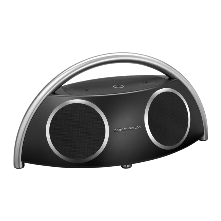
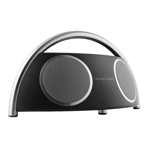
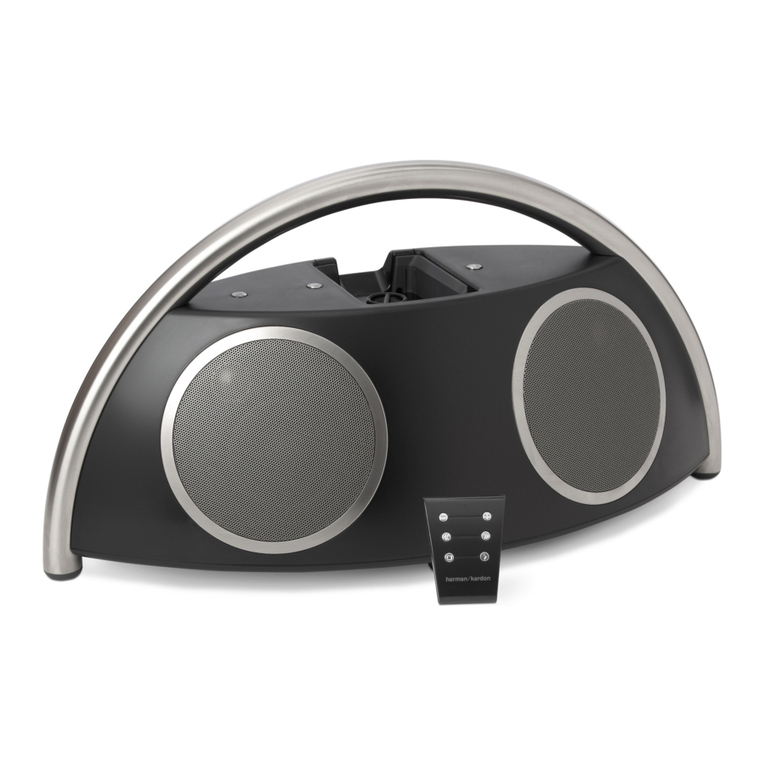
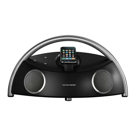
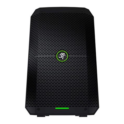
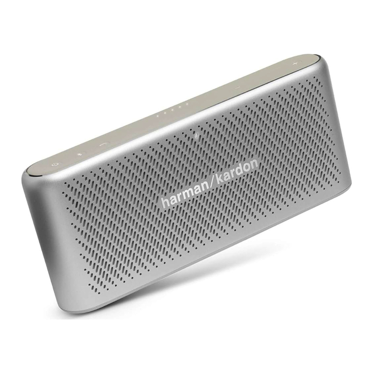
Harman Kardon Go+Play Mini User manual

Harman Kardon Service Manual
Released Globel Quality Harman Consumer Group, Inc. Rev. 1.005/2016
8500 Balboa Boulevard
Northridge, California 91329
CONTENTS Page
Technical Specifications…………....………………………..............2
Safety Instruction, Warning & Notes….……………………....….....3
Set Block Diagram …………..……………………….....……..….….4
Circuit Diagrams
Spare Part list
Revision List
Go+Play Mini
Bluetooth Speaker System with echo and noise cancellation technology and
USB Charge-out.
Set Mechanical Exploded view…................………........….......….8
Set Wiring Diagram
Layout Diagrams.................…......................................................7
Packaging Exploded view………................................…….......….9
……...........................................……………...........10
.................................................................................11
…………..……………………….....……..….…5
....................................…………………....….…..6

· Bluetooth version: 4.2
· Support: A2DP 1.3, AVRCP 1.6, HFP 1.6
· Transducers: 2x woofers (90mm), 2x tweeters (20mm)
· Rated power: 4x25W (AC mode)
· Frequency response: 50Hz-20kHz (-6dB)
· Signal-to-noise ratio: 80dB A-weighted
· Battery type: 22.2Wh rechargeable battery
· Power Supply: 19V 3A
· USB charge out: 5V/2.1A ( 5V/0.5A when playing music)
· Music playtime: up to 5 hours (varies by volume level and audio content)
· Battery charge time: 3 hours
· Dimensions (W x D x H): 417.50mm x 181.50mm x 211.50mm
· Weight: 3433g
· Bluetooth transmitter frequency range: 2402MHz to 2480MHz
· Bluetooth transmitter power: 0 to 9dBm
· Bluetooth transmitter modulation: GFSK, π/4 DQPSK, 8DPSK
TECHNICAL SPECIFICATIONS
2
2

1. Read these instructions.
2. Keep these instructions.
3. Heed all warnings.
4. Follow all instructions.
5. Do not use this apparatus near water.
6. Clean only with a dry cloth.
7. Do not block any ventilation openings.Install in accordance with the manufacturer’s instructions.
8. Do not install near any heat sources such as radiators, heat registers, stoves or other apparatus (including
amplifiers) that produce heat.
9. Do not defeat the safety purpose of the polarized or grounding-type plug. A polarized plug has two blades with one
wider than the other. A grounding-type plug has two blades and a third grounding prong. The wide blade or the
third prong is provided for your safety. If the provided plug does not fit into your outlet, consult an electrician for
replacement of the obsolete outlet.
10. Protect the power cord from being walked on or pinched, particularly at plugs, convenience receptacles and the
point where they exit from the apparatus.
11. Only use attachments/accessories specified by the manufacturer.
12. Use only with the cart, stand, tripod, bracket or table specified by the manufacturer or sold with the
apparatus. When a cart is used, use caution when moving the cart/apparatus combination to avoid
injury from tip-over.
13. Unplug this apparatus during lightning storms or when unused for long periods of time.
14. Refer all servicing to qualified service personnel. Servicing is required when the apparatus has been damaged
in any way, such as power supply cord or plug is damaged, liquid has been spilled or objects have fallen into the
apparatus, or the apparatus has been exposed to rain or moisture, does not operate normally or has been dropped.
15. Do not expose this apparatus to dripping or splashing and ensure that no objects filled with liquids, such as vases,
are placed on the apparatus.
16. To completely disconnect this apparatus from the AC Mains, disconnect the power supply cord plug from the AC
receptacle.
17. The mains plug of the power supply cord shall remain readily operable.
18. Do not expose batteries to excessive heat such as sunshine, fire or the like.
For Products That Transmit and
Receive RF Energy:
FCC Regulations (USA Only)
FCC Information For Users
This device complies with Part 15 of the FCC Rules. Operation
is subject to the following two conditions: (1) This device
may not cause harmful interference; and (2) this device must
accept any interference received, including interference that
may cause undesired operation.
Radio and Television Interference
This equipment has been tested and found to comply with
the limits for a Class B digital device, pursuant to Part 15
of the FCC Rules. These limits are designed to provide
reasonable protection against harmful interference in a
residential installation. This equipment generates, uses and
can radiate radio frequency energy and, if not installed and
used in accordance with the instructions, may cause harmful
interference to radio communications. However, there is no
guarantee that interference will not occur in a particular
installation. If this equipment does cause interference to radio
or television reception, which can be determined by turning
the equipment off and then on, the user is encouraged to try
to correct the interference by one or more of the following
measures:
•Increase the separation between the equipment and
receiver.
•Connect the equipment to a different outlet so that the
equipment and receiver are on different branch circuits.
•Consult the dealer or an experienced radio/TV technician
for help.
NOTE: Changes or modifications not expressly approved
by Harman could void the user’s authority to operate the
equipment.
IC Statement and Warning (Canada Only)
This Class B digital apparatus complies with Canadian ICES-
003. Cet appareil numérique de la classe B est conforme à la
norme NMB-003 du Canada.
For Canadian Model
This Class B digital apparatus complies with Canadian
ICES-003.
Modèle pour les Canadien
Cet appareil numérique de la classe B est conforme à la
norme NMB-003 du Canada.
For Products with Radio Receivers
That Can Use an External Antenna:
CATV or Antenna Grounding
If an outside antenna or cable system is connected to this
product, be certain that it is grounded so as to provide some
protection against voltage surges and static charges. Section
810 of the National Electrical Code, ANSI/NFPA No. 70-1984,
provides information with respect to proper grounding of the
mast and supporting structure, grounding of the lead-in wire
to an antenna discharge unit, size of grounding conductors,
location of antenna discharge unit, connection to grounding
electrodes and requirements of the grounding electrode.
Note to CATV System Installer:
This reminder is provided to call the CATV (cable TV) system
installer’s attention to article 820-40 of the NEC, which
provides guidelines for proper grounding and, in particular,
specifies that the cable ground shall be connected to the
grounding system of the building, as close to the point of
cable entry as possible.
For CD/DVD/Blu-ray Disc™Players:
Caution:
This product uses a laser system. To prevent direct exposure
to the laser beam, do not open the cabinet enclosure or defeat
any of the safety mechanisms provided for your protection.
DO NOT STARE INTO THE LASER BEAM. To ensure proper use
of this product, please read the owner’s manual carefully and
retain it for future use. Should the unit require maintenance
or repair, please contact your local Harman Kardon service
center. Refer servicing to qualified personnel only.
For Products That Include Batteries:
Instructions for Users on Removal and Disposal of
Used Batteries.
CAUTION
Risk of explosion if battery is incorrectly replaced.
Replace only with the same or equivalent type.
Alkaline batteries are considered nonhazardous.
Rechargeable batteries (i.e., nickel cadmium, nickel metal-
hydride, lithium and lithium-ion) are considered hazardous
household materials and may pose an unnecessary health
and safety risk.
In the European Union and other locations, it is illegal to
dispose of any battery with household trash. All batteries
must be disposed of in an environmentally sound manner.
Contact your local waste management officials for information
regarding the environmentally sound collection, recycling and
disposal of used batteries.
To remove the batteries from your equipment or remote
control, reverse the procedure described for inserting
batteries in the owner’s manual.
For products with a built-in battery that lasts for the lifetime of
the product, removal may not be possible for the user. In this
case, recycling or recovery centers handle the dismantling of
the product and the removal of the battery. If, for any reason, it
becomes necessary to replace such a battery, this procedure
must be performed by authorized service centers.
Important Safety Instructions
CAUTION
RISK OF ELECTRIC SHOCK. DO NOT OPEN.
THE LIGHTNING FLASH WITH AN ARROWHEAD SYMBOL,
WITHIN AN EQUILATERAL TRIANGLE, IS INTENDED TO
ALERT THE USER TO THE PRESENCE OF UNINSULATED
“DANGEROUS VOLTAGE” WITHIN THE PRODUCT’S
ENCLOSURE THAT MAY BE OF SUFFICIENT MAGNITUDE TO
CONSTITUTE A RISK OF ELECTRIC SHOCK TO PERSONS.
THE EXCLAMATION POINT WITHIN AN EQUILATERAL
TRIANGLE IS INTENDED TO ALERT THE USER TO
THE PRESENCE OF IMPORTANT OPERATING AND
MAINTENANCE (SERVICING) INSTRUCTIONS IN THE
LITERATURE ACCOMPANYING THE PRODUCT.
WARNING: TO REDUCE THE RISK OF FIRE OR ELECTRIC
SHOCK, DO NOT EXPOSE THIS APPARATUS TO RAIN OR
MOISTURE.
BDS 270 / BDS 570 harman/kardon
2 of 86
3-1
3-1

Each precaution in this manual should be followed during servicing.
Components identified with the IEC symbol in the parts list are special significance to safety. When replacing a component identified with
, use only the replacement parts designated, or parts with the same ratings or resistance, wattage, or voltage that are designated in the
parts list in this manual. Leakage-current or resistance measurements must be made to determine that exposed parts are acceptably
insulated from the supply circuit before retuming the product to the customer.
Some semiconductor (solid state) devices can be damaged easily by static electricity. Such components commonly are called
Electrostatically Sensitive (ES) Devices. Examples of typical ES devices are integrated circuits and some field effect transistors and
semiconductor "chip" components.
The following techniques should be used to help reduce the incidence of component damage caused by static electricity.
1. Immediately before handling any semiconductor component or semiconductor-equipped assembly, drain off any electrostatic charge on
your body by touching a known earth ground. Alternatively, obtain and wear a commercially available discharging wrist strap device,
which should be removed for potential shock reasons prior to applying power to the unit under test.
2. After removing an electrical assembly equipped with ES devices, place the assembly on a conductive surface such as aluminum foil, to
prevent electrostatic charge build-up or exposure of the assembly.
3. Use only a grounded-tip soldering iron to solder or unsolder ES devices.
4. Use only an anti-static solder removal device. Some solder removal devices not classified as "anti-static" can generate electrical charges
sufficient to damage ES devices.
5. Do not use freon-propelled chemicals. These can generate electrical change sufficient to damage ES devices.
6. Do not remove a replacement ES device from its protective package until immediately before you are ready to install it. (Most replacement
ES devices are packaged with leads electrically shorted together by conductive foam, aluminum foil or comparable conductive material.)
7. Immediately before removing the protective material from the leads of a replacement ES device, touch the protective material to the
chassis or circuit assembly into which the device will be installed.
Be sure no power is applied to the chassis or circuit, and observe all other safety precautions.
8. Minimize bodily motions when handling unpackaged replacement ES devices. (Otherwise harmless motion such as the brushing together
or your clothes fabric or the lifting of your foot from a carpeted floor can generate static electricity sufficient to damage an ES devices.
CAUTION :
-2
3-2

SAFETY PRECAUTIONS
The following check should be performed for the continued
protection of the customer and service technician.
LEAKAGE CURRENT CHECK
Measure leakage current to a known earth ground (water
pipe, conduit, etc.) by connecting a leakage current tester
between the earth ground and all exposed metal parts of the
appliance (input/output terminals, screwheads, metal
overlays, control shaft, etc.). Plug the AC line cord of the
appliance directly into a 120V AC 60Hz outlet and turn the
AC power switch on. Any current measured must not exceed
o.5mA.
ANY MEASUREMENTS NOT WITHIN THE LIMITS
OUTLINED ABOVE ARE INDICATIVE OF A
POTENTIAL SHOCK HAZARD AND MUST BE
CORRECTED BEFORE RETURNING THE APPLIANCE
TO THE CUSTOMER.
Device
under
test
Test all
exposed metal
surfaces
Also test with
plug reversed
(Using AC adapter
plug as required)
AC Leakage Test
Leakage
current
tester
Reading should
not be above
0.5mA
Earth
ground
3-3
3-3

•&65
Block Diagram
d
ŶƚĞŶŶĂ
ϰŽŚŵdžϮ
/Ϯ
ƵdžͺŝŶ
ůĂƐƐ
dWϯϭϭϲ
dDŽĚƵůĞ
;
Dϴϳϱ,ǁŝƚŚŽƵƚ
KƚŚĞƌ>Ɛ
DŝĐϮ
ϮϱtϭϱǁdžϮ
E:DϮϳϰϬ
ƵĚŝŽ
^ǁŝƚĐŚ
^ϮϬ
DŝĐϭ
ůĂƐƐ
dWϯϭϭ
ϲ
WDϱϭ
Ϯϭ
/Ϯ^ϭ
ϮϱtϭϱǁdžϮ
ϰŽŚŵdžϮ
WŽǁĞƌdƉůĂLJƉĂƵƐĞ
>
ϭϲďŝƚ
džƉĂŶĚĞƌ
dϭϭϭϲ
WDϱϭ
Ϯϭ
/Ϯ^Ϯ
ƵĚŝŽ
ĚĞƚĞĐƚ
Ϯ
HARMAN INTERNATIONAL. CONFIDENTIAL. COPYRIGHT 2014.
ϭϯϱsƚŽϴsDW
ŚĂƌŐĞ
ƐƚĂƚƵƐ
ĂƚƚĞƌLJ
ĚĞƚĞĐƚ
;
^W/ĨůĂƐŚͿ
^Zϴϲϳϱ
;dĂŶĚDhͿ ŽƚŚĞƌŬĞLJƐ
ĚĂƉƚĞƌŽĨ
ϭϵsϯ ĂƚƚĞƌLJ
ŚĂƌŐĞƌ
YϮϰϲϭϳ
DŝĐϮ
ϳϰs
ϯϬϬϬŵ,
d/
>Dϯϰϴϭ
tŝƚŚ^t
dW^ϱϰϯϯϱ
ϯϯsdϭϭϭϲ
ŽŶƚƌŽů
ĐŚĂƌŐŝŶŐŐ
Audio Signal:
Power Signal:
Control Signal:
KŶŽĨĨ
ƐǁŝƚĐŚ
E:DϮϳϰϬ
džϴW^
dϭϭϭϲ
WŽǁĞƌŬĞLJ
>DZϭϮϬϭϬy
KŶŽĨĨ
ƐǁŝƚĐŚ
dW^Ϯϱϰϲ
&h^tƵƉŐƌĂĚĞ
KŶŽĨĨ
ƐǁŝƚĐŚ
ϭϵsĨŽƌŵƉ
KŶKĨĨ
ƐǁŝƚĐŚ ϯϯs
ϭϴϭ
ĐŚĂƌŐĞŝŶ
ϮϭϬϱ
ĐŚĂƌŐĞŽƵƚ
ϭϵsƚŽDW
KŶŽĨĨ
ƐǁŝƚĐŚ
^ůŐϰϲϭϰϬ
>K
^'DϮϮϬϬ
ϯϯǀĨŽƌϰϲϭϰϬ
ϴW^
E:DϮϳϰϬ
44

Mainboard
LED and Button board
IO Board
RT
RS
LT
LS
RT+
RT-
RS+
RS-
LT+
LT-
LS+
LS-
MIC1 MIC2
9
10
11
12
13
14
15
16
17
8
7
6
5
4
3
2
1
J17
9
10
11
12
13
14
15
16
17
8
7
6
5
4
3
2
1
J13
1
2
3
4
5
6
7
8
9
10
11
12
13
J22
1
2
3
4
5
6
J5
1
2
3
4
5
6
7
J4
1
2
3
4
5
6
7
8
J2
2
1
J11
2
1
J9
SET WIRING DIAGRAM
5
5

160302
05
GO+PLAY MINI
SM
<Checked By>
<QC By>
<Released By>
<Checked Date>
<QC Date>
<Release Date>
<Code> D <Drawing Number>
<Scale> 2 5
REV:SIZE:CODE:
A
B
C
D
DRAWN: DATED:
DATED:CHECKED:
QUALITY CONTROL: DATED:
DATED:RELEASED:
COMPANY:
TITLE:
A
B
C
D
DRAWING NO:
123456
ECO NO:LTR APPROVED: DATE:
REVISION RECORD
SHEET: OFSCALE:
CONNECTED TO BM8675
FAST CHARGE:1.5A
PRECHARGE:60mA
IDPM=3A
0.5A 2.1A
ON
OFF
ON
OFF
ON
OFF
4 1
1A 1.5A
1ACN
2ACP
3/ACDRV
4CE
5STAT1
6TS
18
REFN 17
GND 16
ACSET 15
ISET2 14
SRP 13
SRN
19
LODRV 20
PH 21
HIDRV 22
BTST 23
BATDRV 24
VCC
0EP
12 VFB
11 ISET1
10 VREF
9STAT2
8/PG
7TTC
U6
BQ24617
1S1
2G1
3S2
4G2
8
D1 7
D1 6
D2 5
D2
U12
R19 0R01
R21
100K
1S1
2G1
3S2
4G2
8
D1 7
D1 6
D2 5
D2
U20
PMOS(DUAL)_ME4925_SOP8
C23
104/25V
R22
2R2
C25
225/50V
C26
104/25V C27 104/25V
R23 10R
C28
1UF/25V
C29
102/25V
C30
104/25V
R24
1K
C40
1UF/10V
R25 100R
C53
563/16V
R28 5K62 R37 620R
R38 33K2
R40 12K
C43 104/16V
R51 47K
R15
100K
R13
10K
1
2
3
4
5
J7
CON_XH2.5_5P_V
R52
100K
R53 300K R54 0R
C18 220/16V
C19
106/25V
C21
102/25V
C39
104/25V
R59 33R
R60 33R
C20
106/25V
C56
104/25V
L7 6.8UH
R62
0R01
C57
1UF/25V
C58
104/16V
C59 104/16V
R77 22K
R80 100K
R50 1K8
C95
106/25V
C116
104/16V
C118
104/16V
C121
106/25V
1ISEN
2UVLO
3COMP
4FB
5AGND
10
VIN 9
VCC 8
DR 7
PGND 6
FA/SYN/SD
U7
IC_LM3481_MSOP10
R84 0R01
R91 10R
C126 681/50V
C139
106/25V
C144
102/25V
C145
104/25V
C146
106/25V
R92
0R
C147 106/25V
C148 104/25V
L20 6.8UH
C158 NS
R93 100R
R96 100K
R97 10K
C160 681/50V
C161 103/50V
R95 100K
D5 SK84L
R98 10R
C165681/50V
C166
+C170
220UF/16V/LESR
20%
C171
106/25V
C173
102/25V
C174
104/25V
C175
106/25V
+C176
220UF/25V/LESR
20%
R100 0R
R101
169K
R103
2K2
R104 30K
R105
51K1
Q3
R106 1M
R108
1M R109
100K
C177
NS
R118 10K
R102 33K
Q4
MMBT3904 R119
20K
C178
NS
R120 300K
1IN
2
G
3NC 4
NC
5
OUT
U19
SGM2200-3V3
C179
1UF/25V
C180
1UF/10V
1BOOT
2VIN
3PH
4GND
8
RT 7
EN 6
COMP 5
VSENS 0
EP
U4
IC_TPS54335_SOIC8-EP
1IN
2DM_O
3DP_O
4ILIM_SEL
12
OUT 11
DM_I 10
DP_I 9
/STATUS
13
/FAULT 14
GND 15
ILIM_LO 16
ILIM_HI
8CLT3
7CLT2
6CLT1
5EN
0
PAD
U21
TPS2546
1BST
2GND
3FB
6
SW
5
IN
4
EN
U8
IC_LMR12010X_SOT23-6
D1
L1 4.7UH
C16
22UF/6.3V
C60
100NF/16V
C61
0.1UF/50V
C63
1NF/25V
C64
1NF/25V
C65 103/50V
R8 16.2K L12 600 ohm 1A
L21
600 ohm 1A
C1
106/25V
C3
0.1UF/50V
C4
1NF/25V
C5
106/25V
L22 15UH
C2
476/6V3
C6 104/16V
C7
476/6V3
C8
104/10V
C9
1NF/25V
R1 143K
R3 3K65
C10 121/50V
C15 123/16V
R4 3K92 R9 100K
R10
19K1
C45
1UF/10V
C86
104/10V
R55
100K
R63
100K
R85 NS
R107 100K
R114 100K
R116 100K
R121 NS
R122 NS
R123
750K
R124
84K5
C88
106/25V
C112
104/10V
R125 0R
R129 0R
R130 0R
R131
NS Q5
2N7002
R132 33K
R133 100K
R134 10K
L23 120R/3A
L24 120R/3A
T5
12
D23
Q8
MMBT3904 R269
100K
C243
104/16V
R270 100K
R94
20R
1S
2S
3S
4G
8
D7
D6
D5
D
U32
NMOS_ME4894_SOP8
1S
2S
3S
4G
8
D7
D6
D5
D
U27 ME4435
R268 100K
C242 104/25V
R271 100K
R273
100K C244
103/50V
Q10
D26
R82 10K
R83
30K
R277 300K
Q9
MMBT3904
R272 100K
R274
47K
R276
100K
D28
R6
49.9K
R2 10K
Q12
BAT54C
R5
100K
R20 300K
Q14
BAT54C
Q17
MMBT3904
R215 10K
21
F3
TVS
21
F4
TVS
21
F5
TVS
21
F6
TVS
Q11
MMBT3904
D3
D9
R239
NS
1
2
3
4
5
6
J5
R242 20K
Q22
C195 NS
R99 10K
C103 NS C201 NS
D23-2
R251 NS
R252 NS
L30
Q23
MMBT3904
R220
10K
R233 0R
R253 NS
V_DCIN
GND
GND
GND
GND
GND
GND
CHG_STAT1
CHG_STAT2
GND
BAT_NTC
BAT_NTC
GND
GND
GND
GND GND
GND
GND
V_DCIN_2
GND GND
GND
GND
GND
GND
GNDGND
BIAS_BOOST
V_AMP
GND GND
V_DCIN
GND
V_3V3_SGL46140
GND GND
GND
GND
GND
GND
V_DC-BUCK_IN
GND
V_DC-BUCK_IN
GND
GND
GND
GND
GND
GND
GND
GND
GND
GND
USB_CHARGE_OUT_STAT
GND
USB_CHG_CURRENT_CONTRL
V_3V3_BT+DAC
V_BAT
V_BAT
V_DCIN_2
GND
SD_AMP-POWER
V_DC-BUCK_IN
PWER_ON
GND
GND
V_DCIN
GND
PWER_ON
GND
V_DCIN
HW_RST
HW_RST_2
V_5V_CHARG_OUT
DM
DP
V_DCIN
V_5V_CHARG_OUT
DM
DP
GND
GND
V_BAT
V_DCIN_2
GND
GND
USB_CHG_CURRENT_CONTRL
GND
GND
V_3V3
V_3V3
SDZ_AMP
CIRCUIT DIAGRAM - MAIN BOARD
6
6

05
160302 GO+PLAY MINI
SM
<Checked By>
<QC By>
<Released By>
<Checked Date>
<QC Date>
<Release Date>
<Code> D <Drawing Number>
<Scale> 3 5
REV:SIZE:CODE:
A
B
C
D
DRAWN: DATED:
DATED:CHECKED:
QUALITY CONTROL: DATED:
DATED:RELEASED:
COMPANY:
TITLE:
A
B
C
D
DRAWING NO:
123456
ECO NO:LTR APPROVED: DATE:
REVISION RECORD
SHEET: OFSCALE:
AUXAUDIO DETECT
MIC+
MIC- MIC
MIC+
MIC- MIC
MIC
AUX
USB
CONNECT TO TCA1116
BAT LEVEL DET
SLG46140
MIC
AUX
MUTEUNMUTE
ON
OFF
AMP
0.5A2.1A
TPS2546
ON
NS
NO SIGNAL
BQ24617
OFF ON
1A 1.5A
BQ24617
C150
10NF/50V R110
1M
R111 1M
R112
30K
Q1
MMBT3904
Q2
MMBT3904
R113
2M
R115
15K
C151 1UF/10V
D2 BAS16H
R128 3K9
Q19
MMBT3904
C152 1UF/10V
R117 10K
R127
22.1K
R141
3K9
R142
6k8 R143
200R
R147 3K9
Q27
MMBT3904
C153 1UF/10V
R148 10K
R149
22.1K
R150
3K9
R151
6k8 R152
200R
C167
224/25V
T1 T2 T3 T4
R170
2K
R171
2K
C168
225/10V C169
225/10V
1AIO0
2AIO1
3GND
4I2S1_BCLK
5I2S1_LRCLK
6I2S1_DO
7I2S1_DI
8GND
9SPI_CLK
10 SPI_MISO
11 SPI_CSB
12 SPI_MOSI
13 GND
14 RESET
15 UART_RTS
16 UART_CTS
17 UART_RX
18 UART_TX
19 LED0
20 LED1
21 LED2
22 GPIO8
23 I2C_SDA
24 I2C_SCL
25 GPIO11
26 I2S2_DI
27 I2S2_DO
68
SPK_LP 67
SPK_LN 66
GND 65
MIC_BIAS_A 64
MIC_BIAS_B 63
MIC_LP 62
MIC_LN 61
MIC_RP 60
MIC_RN 59
GND 58
GPIO32 57
GPIO31 56
GPIO30 55
V5V 54
CHG_EXT 53
VBAT_SENSE 52
VBAT 51
1V8 50
VDD_MEM 49
VDD_PADS 48
GND 47
USB_D- 46
USB_D+ 45
GND 44
I2S2_BCLK 43
I2S2_LRCLK 42
GPIO27
69
SPK_RN 70
SPK_RP 71
GND 72
GND 73
RF 74
GND 75
GPIO33
76
GPIO34 77
VDD_3V3 78
GND
41 GPIO26
40 GPIO25
39 GPIO24
38 GPIO23
37 GPIO22
36 GND
35 GPIO21
34 GPIO20
33 GPIO19
32 GPIO18
31 GPIO17
30 GPIO16
29 GPIO15
28 GPIO14
U17
BTM_BM875H_SUNITEC
R7 600R/300mA
R11 33R
R12 33R
G
G
FB
J1
C24 NS
R14
0R
C22 NS
R16 600R/300mA
R17 33R
R18 33R
R41 4R7
C66
104/10V
C67
225/10V
C68
102/25V
C69 104/10V
C72
104/10V
C94
102/25V
C83 104/10V
R44 100K
R42 0R
R45 NS
C17
1UF/10V
F1 220R/0.3A
R46 10R
C193
220/50V
C194 100NF/16V
C196
2.2UF/10V
C197
33PF/50V
R198 1K
C198
2.2UF/10V
R199
2.2K
C199
220/50V
C200 100NF/16V
C202
2.2UF/10V
C203
33PF/50V
R200 1K
C204
2.2UF/10V
R201
2.2K
R202 0R
C205
104/10V
C207 4.7UF/6.3V
Q6
R206
NS
R207
NS
C209
103/50V
C210
NS
C211 NS
R47 1K
R48 1K
R243
4K7
R244
4K7
R247 34K8
R248 200K
R249 100K
C239 103/50V
C208 4.7UF/6.3V
C206 4.7UF/6.3V
C240 4.7UF/6.3V
R203 0R
R205 0R
R258 20R
R259 20R
R204 10K
C265
104/10V
C266
104/10V
C267
104/10V
C268
104/10V
C269
104/10V
R313 0R
R314 0R
R315 0R
R316 0R
R317 0R
Q15
MMBT3904
Q16
MMBT3904
R320 470K
R318
100K
Q18
MMBT3904
C220
1UF/10V
R216
100K
1VDD
2GPI
3GPIO
4GPIO
5GPIO
6GPIO
7GPIO
14
GPIO 13
GPIO 12
GPIO 11
GPIO 10
GPIO 9
GPIO 8
GND
U2
IC_SLG46140_QFN14(1.6X2.0MM)
R135 33R
R136 1K
R137 33R
R138 33R R139 33R
R140 33R
R144 0R
R145 0R
R146 0R
C113
104/10V
C115
106/25V
R154 1K
R155 24K3 R156 10K R157 0R
R159 82K R160 470K
21
F10
TVS
21
F11
TVS
R126 1M
R217 1M
R218 1M
R219 10K
2
31
Q20
BAT54C
Q7
R221 100K
Q21
MMBT3904
R222 100K
R223
0R
R224 NS
9
10
11
12
13
14
15
16
17
8
7
6
5
4
3
2
1
J13
CON_FPC0.5_17P_V_+
T6
T7
2
1
J11
CON_ZH1.5_2P_H
2
1
J9CON_ZH1.5_2P_H
R81 NS
1V+
2NO1
3COM1
4IN1
5NC1
10
NO2 9
COM2 8
IN2 7
NC2 6
GND
U26
IC_SD20_QFN10(1.4X1.8MM)
R153 NS
1INT
2A1
3RESET
4P00
5P01
6P02
7P03
8P04
9P05
10 P06
11 P07
12 GND
24
VCC 23
SDA 22
SCL 21
A0 20
P17 19
P16 18
P15 17
P14 16
P13 15
P12 14
P11 13
P10
U1
IC_TCA1116_TSSOP24
C212 4.7UF/6.3V
C213 104/10V
F2 10R
R246 0R
C238 104/10V
R323
10K
R324
10K
R328
10K
R329
10K
R245
4K7
R158 3k32
R238 3k32
R240
6k8
R241
6k8
21
F7
TVS
21
F8
TVS
21
F9
TVS
1
2
3
4
5
6
7
J4
1
2
3
4
5
6
J3
R250 NS
+C221
470U/6V3
R36
10K
C222 NS
L29 600 ohm 1A
L31 600 ohm 1A
R256
2M
C223 1UF/10V
C224 102/25V
C225
103/50V
C232
103/50V
C233
103/50V
C234
103/50V
C235
103/50V
C236
103/50V
C237
103/50V
C241
103/50V
C251
103/50V
C252 103/50V
D4
BAS16H
V_3V3_BT+DAC
AUD_DET
GND GND GND
V_3V3_BT+DAC
V_3V3_BT+DAC
V_3V3_BT+DAC
GND GND
GND GND
GND
AUX_IN_L_DET
AUX_IN_R_DET
GND
GND
I2S_BCLK_BT1
I2S_LRCLK_BT1
I2S_DATA_BT1
GND
GND
GND
I2S_BCLK_BT2
I2S_LRCLK_BT2
I2S_DATA_BT2
V_3V3_BT+DAC
MIC_BIAS_B
MIC_BIAS_A
MIC_BIAS_A
MIC1
MIC_BIAS_B
MIC2
MIC1
AUX_IN_L
GND
MIC2
MIC_LP
MIC_LP
MIC_RP
MIC_RP
V_3V3_BT+DAC
GND
SOURCE_SEL
I2C_SDA
I2C_SCL
GND
GND
V_3V3_BT+DAC
VREG_EN VREG_EN
IO_RESET
IO_INT
GND
V_BAT
V_1V8 AUX_IN_R
GND
GND
GND
GND
GND
GND
POWER_ON/OFF
POWER_OFF_READY
DC_DET
MUTE_REQ
SOURCE_SEL
V_3V3_BT+DAC
GND
KEY_BT
KEY_VOL-
KEY_VOL+
KEY_PHONE
LED_BT
LED_POWER
LED_PHONE
LED_BAT1_RED
LED_BAT1
LED_BAT2
LED_BAT3
LED_BAT4
V_3V3_SGL46140
GNDGND
V_3V3_SGL46140
KEY_VOL+
KEY_VOL-
KEY_PHONE
HW_RST
GND
HW_RST_2
A
POWER_OFF_READY
BIAS_BOOST
POWER_ON/OFF
V_3V3_SGL46140
GND
V_3V3_BT+DAC GND
PWER_ON
MUTE_REQ
VREG_EN
GND V_DCIN
DC_DET
USB_5V
USB_D-
USB_D+
AUX_IN_R
AUX_IN_L
GND
KEY_POWER
KEY_POWER
GND
LED_BAT5
LED_POWER
LED_BT
LED_PHONE
V_1V8
GND
SDZ_AMP
MUTE_AMP
V_3V3_BT+DAC
GND
I2C_SDA
I2C_SCL
AUD_DET
GND
GND
V_3V3_BT+DAC
GND
GND
IO_INT
IO_RESET
GND
CHG_STAT1
CHG_STAT2
V_3V3_BT+DAC
SD_AMP-POWER
USB_CHARGE_OUT_STAT
USB_CHG_CURRENT_CONTRL
V_3V3_BT+DAC
KEY_VOL+
KEY_PHONE
LED_BAT1_RED
KEY_BT
KEY_VOL-
LED_BAT1
LED_BAT2
LED_BAT3
LED_BAT4
LED_BAT5
USB_5V
USB_D-
USB_D+
GND
GND
AUX_IN_R_DET
AUX_IN_L_DET
SPI_CSB
SPI_CLK
SPI_MISO
SPI_MOSI
GND
GND
CIRCUIT DIAGRAM - MAIN BOARD

160302
05
SM
<Checked By>
<QC By>
<Released By>
<Checked Date>
<QC Date>
<Release Date>
GO+PLAY MINI
<Code> D <Drawing Number>
<Scale> 4 5
REV:SIZE:CODE:
A
B
C
D
DRAWN: DATED:
DATED:CHECKED:
QUALITY CONTROL: DATED:
DATED:RELEASED:
COMPANY:
TITLE:
A
B
C
D
DRAWING NO:
123456
ECO NO:LTR APPROVED: DATE:
REVISION RECORD
SHEET: OFSCALE:
L CH
R CH
CONNECTED TO BM8675H
ENABLE
MUTE
SD
LT
LS
RT
RS
RT
RS
LT
LS
Sub_L
Sub_R
Trib_R
Trible_L
I2C ADR 11
I2C ADR 01
1MODSEL
2SDZ
3FAULTZ
4RINP
5RINN
6PLIMIT
7GVDD
8GAIN/SLV
9GND
10 LINP
11 LINN
12 MUTE
13 AM2
14 AM1
15 AM0
16 SYNC
32
PVCC 31
PVCC 30
BSPR 29
OUTPR 28
GND 27
OUTNR 26
BSNR 25
GND 24
BSPL 23
OUTPL 22
GND 21
OUTNL 20
BSNL 19
PVCC 18
PVCC 17
AVCC
U10
IC_TPA3116D2_HTSSOP32-UP
R64 100K
R65 20K
C76
1UF/16V
C77 225/10V
C78 225/10V
C79 225/10V
C80 225/10V
R67 100K
L3 6.8UH
C82
102/25V
R68
3.3R
R69
3.3R
C87 0.22UF/25V
C85
102/25V
C89 0.22UF/25V
C90
0.68UF/25V
C91
102/25V
C92
10NF/50V(NS)
R70
3.3R
R71
3.3R
C96
0.68UF/25V
C97
102/25V
C98 0.22UF/25V
C99 0.22UF/25V
+C100
100UF/25V/LESR
C101
104/25V
C102
102/25V
C104
104/25V
C105
102/25V
1MODSEL
2SDZ
3FAULTZ
4RINP
5RINN
6PLIMIT
7GVDD
8GAIN/SLV
9GND
10 LINP
11 LINN
12 MUTE
13 AM2
14 AM1
15 AM0
16 SYNC
32
PVCC 31
PVCC 30
BSPR 29
OUTPR 28
GND 27
OUTNR 26
BSNR 25
GND 24
BSPL 23
OUTPL 22
GND 21
OUTNL 20
BSNL 19
PVCC 18
PVCC 17
AVCC
U16
IC_TPA3116D2_HTSSOP32-UP
R72 47K
R73 75K
C106
1UF/16V
C107 225/10V
C108 225/10V
C109 225/10V
C110 225/10V
C124
102/25V
R78
3.3R
R79
3.3R
C130
102/25V
C131 0.22UF/25V
C132 0.22UF/25V
C134
104/25V
C135
102/25V
C137
104/25V
C138
102/25V
L4 6.8UH
C62
0.68UF/25V
C71
0.68UF/25V
C73
10NF/50V(NS)
C74
10NF/50V(NS)
C75
10NF/50V(NS)
C81
10NF/50V(NS)
C84
10NF/50V(NS)
C93
0.68UF/25V
C111
0.68UF/25V
1
2
3
4
5
6
7
8
J2
R27
1K
C13
225/10V
C14
225/10V
R30
1K
C32
102/25V
C33
104/16V
C34
10UF/6.3V
R31
0R
R32
0R
R33
NS
R34
0R
C11
104/16V
C12
102/25V
C35
104/16V
C36
102/25V
R35
0R C37
104/16V
C31
102/25V
R26
0R
R87
0R
R39
1K
C38
225/10V
C41
225/10V
R43
1K
C42
102/25V
C44
104/16V
C46
10UF/6.3V
R56
0R
R57
0R
R58
0R
R61
0R
C47
104/16V
C48
102/25V
C49
104/16V
C50
102/25V
R76
0R C51
104/16V
C52
102/25V
R86
0R
R88
0R
L2 6.8UH
C54
102/25V
R89
3.3R
R90
3.3R
C55 0.22UF/25V
C70
102/25V
C114 0.22UF/25V
L19 6.8UH
C140
0.68UF/25V
C141
0.68UF/25V
C142
10NF/50V(NS)
C143
10NF/50V(NS)
+
-
8
VCC
4G
U5-A
NJM2740
+
-
3
21
U5-B
NJM2740
C117 4.7UF/6.3V
R161 10K
R162 10K
C119 680/50V
R163 10K
R164 0R
C120
104/10V
+
-
5
67
U5-C
NJM2740
C122 4.7UF/6.3V
R165 10K
R166 10K
C123 680/50V
R167 10K
+
-
3
21
U13-B
NJM2740
C127 1UF/10V
R168 10K
+
-
5
67
U13-C
NJM2740
C128 1UF/10V
R169 10K
+
-
3
21
U14-B
NJM2740
C129 4.7UF/6.3V
R172 10K
+
-
5
67
U14-C
NJM2740
C149 4.7UF/6.3V
R173 10K
R174 0R
+
-
3
21
U22-B
NJM2740
C154 4.7UF/6.3V
R175 10K
R176 10K
C155 680/50V
R177 10K
+
-
5
67
U22-C
NJM2740
C156 4.7UF/6.3V
R178 10K
R179 10K
C157 680/50V
R180 10K
+
-
3
21
U23-B
NJM2740
C159 1UF/10V
R181 10K
+
-
5
67
U23-C
NJM2740
C162 1UF/10V
R182 10K
+
-
3
21
U24-B
NJM2740
C163 4.7UF/6.3V
R183 10K
+
-
5
67
U24-C
NJM2740
C164 4.7UF/6.3V
R184 10K
R185 0R
R186
0R
R187
100K
R188
1M
R189
133K
C172
106/25V
R190 0R
R191
0R
+
-
8
VCC
4G
U13-A
NJM2740
R192 0R
C181
104/10V
C182
10UF/6.3V
+
-
8
VCC
4G
U14-A
NJM2740
R193 0R
C183
104/10V
C184
10UF/6.3V
R194
1K
R195
1K
C185
104/10V
C186
10UF/6.3V
C187
104/10V
C188
10UF/6.3V
R196
1K
R197
1K
C189
104/10V
C190
10UF/6.3V
C191
104/10V
C192
10UF/6.3V
+
-
3
21
U28-B
NS
C214 NS R49 NS
R208 NS
C215 NS
R209 NS R210 NS
C216 NS
+
-
5
67
U28-C
NS
C217 NS R211 NS
R212 NS
C218 NS
R213 NS R214 NS
C219 NS
+
-
3
21
U30-B
NS
C226 NS R225 NS
R226 NS
C227 NS
R227 NS R228 NS
C228 NS
+
-
5
67
U30-C
NS
C229 NS R229 NS
R230 NS
C230 NS
R231 NS R232 NS
C231 NS
+
-
84
U22-A
NJM2740
R29 0R
C125
104/10V
+
-
8
VCC
4G
U23-A
NJM2740
R278 0R
C245
104/10V
C246
10UF/6.3V
+
-
8
VCC
4G
U24-A
NJM2740
R279 0R
C247
104/10V
C248
10UF/6.3V
+
-
8
VCC
4G
U28-A
NS
R280 NS
C249
NS
+
-
8
VCC
4G
U30-A
NS
R281 NS
C250
NS
R284 10K
R285 10K
Q13
MMBT3904
R66
10K
R286 100K
C253 104/10V
C254 104/10V
C255 104/10V
R74 10K
R75 100K
R295
33R
C256 121/50V
R296
0R
R297
NS
R298
0R
R299
NS
C257
NS
C259
NS
C261
NS
C263
NS
R234
0R
R235
0R
R236
0R
R237
0R
+C133
220UF/25V/LESR
+C136
100UF/25V/LESR
R287
0R
R291
0R
D6
D10
D8
D7
L26 6.8
L25 6.8
L27 6.8
L28 6.8
Q24
BAT54C
3
CPGND 4
CAPM 5
VNEG 6
OUTL 7
OUTR 8
AVDD 9
AGND 10
VCOM 11
SDA 12
SCL 13
GPIO5 14
GPIO4
26 LDOO
25 XSMT
24 ADR1
23 LRCK
22 DIN
21 BCK
20 SCK
19 GPIO6
18 MODE2
17 MODE1
16 ADR2
15 GPIO3
2
CAPP 1
CPVCC
28 DVDD
27 DGND
U11
IC_PCM5121_TSSOP28
3
CPGND 4
CAPM 5
VNEG 6
OUTL 7
OUTR 8
AVDD 9
AGND 10
VCOM 11
SDA 12
SCL 13
GPIO5 14
GPIO4
26 LDOO
25 XSMT
24 ADR1
23 LRCK
22 DIN
21 BCK
20 SCK
19 GPIO6
18 MODE2
17 MODE1
16 ADR2
15 GPIO3
2
CAPP 1
CPVCC
28 DVDD
27 DGND
U3
IC_PCM5121_TSSOP28
1
2R254
0R
R255
0R
R257
1K
R260
1K
R261
1K
R262
1K
GND
SDZ_AMP
GND
MUTE_AMP
GND
GND
GND
GND
GND GND
GND GND
V_AMP
GND GND GND
V_AMP
GNDGND
GND
GND
GND
GND
GND
GND
GND GND
V_AMP
GND GND GND
V_AMP
GNDGNDGND
GND
GND GND GND
GND
I2S_BCLK_BT1
I2S_DATA_BT1
I2S_LRCLK_BT1
V_3V3_BT+DAC
GND
GND
GND
GND
GND GND GND
GND
I2S_BCLK_BT2
I2S_DATA_BT2
I2S_LRCLK_BT2
V_3V3_BT+DAC
GND
GND
GND
GND
GND GND
DAC_OUTR1
DAC_OUTL1
DAC_OUTL1
BIAS_OPAMP1
GNDGND
V_3V3_BT+DAC
DAC_OUTR1
BIAS_OPAMP1
BIAS_OPAMP1
BIAS_OPAMP1
BIAS_OPAMP1
DAC_OUTL1
BIAS_OPAMP1
DAC_OUTR1
DAC_OUTR2
DAC_OUTL2
DAC_OUTL2
BIAS_OPAMP2
DAC_OUTR2
BIAS_OPAMP2
BIAS_OPAMP2
BIAS_OPAMP2
BIAS_OPAMP2
DAC_OUTL2
BIAS_OPAMP2
DAC_OUTR2
GND
V_3V3_BT+DAC
GND
A
GNDGND GNDGND
GND
V_3V3_BT+DAC
BIAS_OPAMP1
GND
V_3V3_BT+DAC
BIAS_OPAMP2
DAC_OUTR1
BIAS_OPAMP1
GND
DAC_OUTL1
BIAS_OPAMP1
GND
DAC_OUTR1_DELAY
DAC_OUTL1_DELAY
DAC_OUTR2
BIAS_OPAMP2
GND
DAC_OUTL2
BIAS_OPAMP2
GND
DAC_OUTR2_DELAY
DAC_OUTL2_DELAY
DAC_OUTR2_DELAY
DAC_OUTR1_DELAY
DAC_OUTL2_DELAY
DAC_OUTL1_DELAY
GNDGND GNDGND GNDGND GNDGND GNDGND
GND
SDZ_AMP
V_3V3_BT+DAC
V_3V3_BT+DAC
GND
GND
GND V_GVDD
V_GVDD
V_3V3_BT+DAC
GND
GND
GND
I2C_SDA
I2C_SCL
CIRCUIT DIAGRAM - MAIN BOARD

SCALE: SHEET: OF
REVISION RECORD
DATE:APPROVED:LTR ECO NO:
654321
DRAWING NO:
D
C
B
A
TITLE:
COMPANY:
RELEASED: DATED:
DATED:QUALITY CONTROL:
CHECKED: DATED:
DATED:DRAWN:
D
C
B
A
CODE: SIZE: REV:
11<Scale>
01<Drawing Number>D<Code>
GO+PLAY MINI
<Release Date>
<QC Date>
<Checked Date>
<Drawn Date>
<Released By>
<QC By>
<Checked By>
SM
PWR
BT
VOL-
VOL+
PHONE
LED_BAT2
LED_BAT1
LED_BAT3
LED_BAT4
LED_PHONE
LED_BT
LED_Pwr
LED_BAT1_RED
V_3V3_SGL46140
V_3V3_BT+DAC
TP1 TP2
23
S1
S2
S3
S4
S5
R300 470R
R301 470R
R302 470R
R303 470R
R304 470R
R305 470R
R306 470R
R307 470R
R308
10K
R309
10K
R310
NS
R311
10K
R312
10K
R238 470R
D18
D19
D20
D21
D22
D14
9
10
11
12
13
14
15
16
17
8
7
6
5
4
3
2
1
COJ1N7_FPC0.5_17P_V_+
D15
D16
D17
D1 NS R1 NS
D2 NS R2 NS
GND
CIRCUIT DIAGRAM - LED BOARD

TYPE A
MICRO USB
2
3
1
J14
JACK_DC_10-9.5_001
1
VCC 2
D- 3
D+ 4
GND 5
SHIELD
J15
USB_SOCKET_TYPE-A_HI
1
VCC 2
D- 3
D+ 4
GND 5
SHIELD
J16
USB_SOCKET_MICRO_SMD_H_1
R252 R251
C195
NS
R253
R254
R255 R256
NS
C201
NS
R257
NS
C241
NS
R260 0R
R261 0R
R262 0R
R263 NS
R264
R265
R266
R267
TP1 TP2
1
2
3
4
5
6
7
8
9
10
11
12
13
J22
1
G6
62
R4
45
53
L
J1
JACK/HP/6P-2
GND
V_DCIN
GND
AUX_IN_R
AUX_IN_L
GND
CIRCUIT DIAGRAM - IO BOARD

LAYOUT DIAGRAM - MAIN BOARD
7

LAYOUT DIAGRAM - LED BOARD

LAYOUT DIAGRAM - IO BOARD

32 TT0020033010 FOOT PAD RING BLK GO+PLAY MINI
32 TT0020033020 FOOT PAD RING WHT GO+PLAY MINI
31 TT0020032010 FOOT PAD BLK GO+PLAY MINI
31 TT0020032020 FOOT PAD WHT GO+PLAY MINI
30 MM0402001010 BOTTOM CASE BLK GO+PLAY MINI
30 MM0402001020 BOTTOM CASE WHT GO+PLAY MINI
26 APA2PLAYM0101 MAIN BOARD GO+PLAY MINI
25 EXA3030007410 Li-ion BATTERY GO+PLAY MINI
23 GL0144001010 BATTERY CASE GO+PLAY MINI
22 APA2PLAYM0201 IO BOARD GO+PLAY MINI
21 ZS0045002010 SEALING STRIP GO+PLAY MINI
19 HZ0407001010 REAR COVER BLK GO+PLAY MINI
19 HZ0407001020 REAR COVER WHT GO+PLAY MINI
18 GL0071001010 I/O CASE BLK GO+PLAY MINI
18 GL0071001020 I/O CASE WHT GO+PLAY MINI
17 WT0417001010 REAR FABRIC GRILL BLK GO+PLAY MINI
17 WT0417001020 REAR FABRIC GRILL WHT GO+PLAY MINI
15 DQ0015007010 GASKET GO+PLAY MINI
14 BS1312001010 HANDLE GO+PLAY MINI
13 MZ0262003010 RUBBER BUTTON BLK GO+PLAY MINI
13 MZ0262003020 RUBBER BUTTON WHT GO+PLAY MINI
12 JL0105001010 BUTTON GO+PLAY MINI
11 ZJ0253001010 BUTTON CASE BLK GO+PLAY MINI
10 APA2PLAYM0301 KEY BOARD GO+PLAY MINI
7 000100 14201 1 PASSIVE RADIATOR WHT GO+PLAY MINI
7 000100 20001 1 PASSIVE RADIATOR BLK GO+PLAY MINI
6 320019 01504 TWEETER GO+PLAY MINI
5 110092 02301 WOOFER GO+PLAY MINI
4 MZ0407001010 FRONT COVER BLK GO+PLAY MINI
4 MZ0407001020 FRONT COVER WHT GO+PLAY MINI
1 WT0417002010 FRONT FABRIC GRILL ASSY BLK GO+PLAY MINI
1 WT0417002020 FRONT FABRIC GRILL ASSY WHT GO+PLAY MINI
noitpircseDN/P.oN.soP
MECHANICAL EXPLODED VIEW
8

PACKAGING VIEW 9

HK GO+PLAY MINI SPARE PARTS LIST
Pos. No. P/N Description
1 WT0417002010 FRONT FABRIC GRILL ASSY BLK GO+PLAY MINI
1 WT0417002020 FRONT FABRIC GRILL ASSY WHT GO+PLAY MINI
4 MZ0407001010 FRONT COVER BLK GO+PLAY MINI
4 MZ0407001020 FRONT COVER WHT GO+PLAY MINI
5 110092 02301 WOOFER GO+PLAY MINI
6 320019 01504 TWEETER GO+PLAY MINI
7 000100 14201 1 PASSIVE RADIATOR WHT GO+PLAY MINI
7 000100 20001 1 PASSIVE RADIATOR BLK GO+PLAY MINI
10 APA2PLAYM0301 KEY BOARD GO+PLAY MINI
11 ZJ0253001010 BUTTON CASE BLK GO+PLAY MINI
12 JL0105001010 BUTTON GO+PLAY MINI
13 MZ0262003010 RUBBER BUTTON BLK GO+PLAY MINI
13 MZ0262003020 RUBBER BUTTON WHT GO+PLAY MINI
14 BS1312001010 HANDLE GO+PLAY MINI
15 DQ0015007010 GASKET GO+PLAY MINI
17 WT0417001010 REAR FABRIC GRILL BLK GO+PLAY MINI
17 WT0417001020 REAR FABRIC GRILL WHT GO+PLAY MINI
18 GL0071001010 I/O CASE BLK GO+PLAY MINI
18 GL0071001020 I/O CASE WHT GO+PLAY MINI
19 HZ0407001010 REAR COVER BLK GO+PLAY MINI
19 HZ0407001020 REAR COVER WHT GO+PLAY MINI
21 ZS0045002010 SEALING STRIP GO+PLAY MINI
22 APA2PLAYM0201 IO BOARD GO+PLAY MINI
23 GL0144001010 BATTERY CASE GO+PLAY MINI
25 EXA3030007410 Li-ion BATTERY GO+PLAY MINI
26 APA2PLAYM0101 MAIN BOARD GO+PLAY MINI
30 MM0402001010 BOTTOM CASE BLK GO+PLAY MINI
30 MM0402001020 BOTTOM CASE WHT GO+PLAY MINI
31 TT0020032010 FOOT PAD BLK GO+PLAY MINI
31 TT0020032020 FOOT PAD WHT GO+PLAY MINI
32 TT0020033010 FOOT PAD RING BLK GO+PLAY MINI
32 TT0020033020 FOOT PAD RING WHT GO+PLAY MINI
ETSN1024A5W0N AC ADAPTER 19V 3A WHT GO+PLAY MINI
ETSN1024B2B0NS AC ADAPTER 19V 3A BLK GO+PLAY MINI
EWA6HMMGP0010 RF ANTENNA GO+PLAY MINI
EWB5017001000 13P CABLE GO+PLAY MINI
EWF2013090170 17P FFC CABLE GO+PLAY MINI
EWP0120007020 EU POWER CORD BLK GO+PLAY MINI
EWP0120097030 EU POWER CORD WHT GO+PLAY MINI
EWP1120007121 US POWER CORD BLK GO+PLAY MINI
EWP1120097130 US POWER CORD WHT GO+PLAY MINI
EWP2120007221 UK POWER CORD BLK GO+PLAY MINI
EWP2120097230 UK POWER CORD WHT GO+PLAY MINI
EWP4120007B21 KOR POWER CORD BLK GO+PLAY MINI
EWP4120097B30 KOR POWER CORD WHT GO+PLAY MINI
EWP5120007421 CHN POWER CORD BLK GO+PLAY MINI
EWP5120097K30 CHN POWER CORD WHT GO+PLAY MINI
10

EWP8120097D30 THAILAND POWER CORD BLK GO+PLAY MINI
EWPF120007L21 THAILAND POWER CORD WHT GO+PLAY MINI
EWPE120007521 AUS POWER CORD BLK GO+PLAY MINI
EWPE120097530 AUS POWER CORD WHT GO+PLAY MINI
EXM0304150010 MIC GO+PLAY MINI

REVISION LIST
Version 1.0
Initial release for HK GO+PLAY MINI May 2016
11
Other Harman Kardon Portable Speakers manuals

Harman Kardon
Harman Kardon TRAVELER User manual

Harman Kardon
Harman Kardon Go+Play Micro User manual

Harman Kardon
Harman Kardon JBL Link 20 User manual

Harman Kardon
Harman Kardon JBL TUNER XL User manual

Harman Kardon
Harman Kardon Go+Play User manual

Harman Kardon
Harman Kardon AVR 7500 User manual

Harman Kardon
Harman Kardon GO + P L AY WIRELESS User manual

Harman Kardon
Harman Kardon Go+Play User manual

Harman Kardon
Harman Kardon HKGOPLAY User manual

Harman Kardon
Harman Kardon Go + Play II User manual