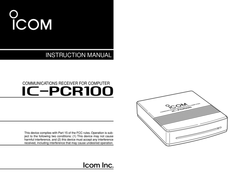
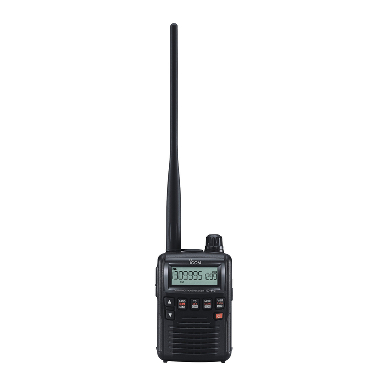
Icom COMMUNICATION RECEIVER IC PCR100 User manual

SERVICE
MANUAL
COMMUNICATION
RECEIVER FOR COMPUTER
iC-pcr100

REPAIR NOTES
1. Make sure a problem is internal before disassembling
the receiver.
2. DO NOT open the receiver until the receiver is discon-
nected from its power source.
3. DO NOT force any of the variable components. Turn
them slowly and smoothly.
4. DO NOT short any circuits or electronic parts. An insu-
lated tuning tool MUST be used for all adjustments.
5. DO NOT keep power ON for a long time when the
receiver is defective.
6. READ the instructions of test equipment thoroughly
before connecting equipment to the receiver.
INTRODUCTION DANGER
This service manual describe the latest service information
for the IC-PCR100 COMMUNICATION RECEIVER FOR
COMPUTER at the time of publication.
NEVER connect the receiver to an AC outlet or to a DC
power supply that uses more than 16 V. Such a connection
could cause a fire hazard and/or electric shock.
DO NOT expose the receiver to rain, snow or any liquids.
DO NOT reverse the polarities of the power supply when
connecting the receiver.
DO NOT apply an RF signal of more than 20 dBm (100
mW) to the antenna connector. This could damage the
receiver’s front end.
Be sure to include the following four points when ordering
replacement parts:
1. 10-digit order numbers
2. Component part number and name
3. Equipment model name and unit name
4. Quantity required
<SAMPLE ORDER>
1130004200 S.IC TC4S66F IC-PCR100 MAIN UNIT 1 piece
8810008660 Screw PH B0 3
×
8 NI-ZU IC-PCR100 CHASSIS 4 pieces
Addresses are provided on the inside back cover for your
convenience.
ORDERING PARTS
To upgrade quality, any electrical or mechanical parts and
internal circuits are subject to change without notice or
obligation
MODEL
IC-PCR100
Europe
U.K.
Canada
U.S.A-1
Other
EUR
UK
CAN
USA-1
OTH
VERSION SYMBOL

TABLE OF CONTENTS
SECTION 1 SPECIFICATIONS
SECTION 2 INSIDE VIEWS
SECTION 3 DISASSEMBLY INSTRUCTIONS
SECTION 4 CIRCUIT DESCRIPTION
4 - 1 RECEIVER CIRCUITS............................................................................................................................. 4 - 1
4 - 2 PLL CIRCUITS........................................................................................................................................ 4 - 4
4 - 3 POWER SUPPLY CIRCUITS.................................................................................................................. 4 - 5
4 - 4 CPU PORT ALLOCATIONS
.................................................................................................................... 4 - 6
SECTION 5 ADJUSTMENT PROCEDURES
5 - 1 PREPARATION BEFOR SERVICING ..................................................................................................... 5 - 1
5 - 2 PLL ADJUSTMENTS .............................................................................................................................. 5 - 3
5 - 3 IF PEAK AND TOTAL GAIN ADJUSTMENTS
....................................................................................... 5 - 5
5 - 4 SOFTWARE ADJUSTMENTS
................................................................................................................ 5 - 7
SECTION 6 PARTS LIST
SECTION 7 MECHANICAL PARTS AND DISASSEMBLY
SECTION 8 SEMI-CONDUCTOR INFORMATION
SECTION 9 BOARD LAYOUTS
9 - 1 MAIN UNIT.............................................................................................................................................. 9 - 1
SECTION 10 BLOCK DIAGRAM
SECTION 11 VOLTAGE DIAGRAM
11 - 1 MAIN UNIT
............................................................................................................................................ 11 - 1

MGENERAL
• Frequency range :
*Specifications guaranteed 0.5–1300 MHz only
• Mode : AM, FM, WFM
• Frequency stability : ±5 ppm (at 1300 MHz: ±0˚C to +50˚C; +32˚F to +122˚F)
• Frequency resolution : 1 kHz (minimum)
• Power supply requirement : 13.8 V DC ±15 % for receiver unit; or supplied AC adaptor (negative ground)
• Current drain (at 13.8 V DC) : Power ON (PC power OFF) 0.1 A
Max. audio 0.7 A
Standby (squelched) 0.6 A
• Usable temperature range : ±0˚C to +50˚C; +32˚F to +122˚F
• Antenna connector : BNC (50 Ω)
• RS-232C connector : D-sub 9-pin (female)
• Dimensions : 131(W)✕35(H)✕164.1(D) mm;
55⁄32(W)✕13⁄8(H)✕615⁄32(D) inch
• Weight : approx. 0.5 kg; 1 lb 2 oz
MRECEIVER
• Receive system : Triple-conversion superheterodyne
• Intermediate frequency : 1st 266.7 MHz
2nd 10.7 MHz
3rd 450 kHz (except WFM)
• Sensitivity (typical)* :
• Squelch sensitivity :
(at threshold)
• Selectivity (typical) : WFM 230 kHz/–6 dB
WFM/FM/AM 50 kHz/–6 dB
FM/AM 15 kHz/–6dB
FM/AM/SSB/CW 6 kHz/–6 dB
• Max audio output : Mono 200 mW
(at 10% distortion with an 8Ωload) Stereo 100 mW
• External speaker connector : 3-conductor 3.5(d) mm (1⁄8")/4–8 Ω
Frequency
[MHz]
0.5 – 1.799
1.8 – 27.999
28.0 – 29.999
30.0 – 49.999
50.0 – 699.999
700.0 –1300.000
1 - 1
SECTION 1 SPECIFICATIONS
Version Frequency Range (MHz)
0.010 – 823.999*
U.S.A.-1 849.001 – 868.999
894.001 – 1300.000
Europe, U.K. 0.010 – 1300.000*
Canada Other
FM
—
0.5 µV
0.32 µV
0.4 µV
AM
2.5 µV
1.8 µV
1.0 µV
1.3 µV
WFM
—
0.79 µV
1.0 µV
*FM and WFM are measured at 12 dB SINAD; AM is measured at
10 dB S/N.; 230 kHz (for WFM), 15 kHz (for FM) and 6 kHz (for
AM) passband widths are selected.
Frequency
[MHz]
0.5 – 1.799
1.8 – 27.999
28.0 – 29.999
30.0 – 49.999
50.0 – 699.999
700.0 –1300.000
FM
—
0.63 µV
0.5 µV
0.63 µV
WFM
—
5.6 µV
10 µV
AM
1.8 µV
0.89 µV
0.71 µV
0.89 µV

2 - 1
SECTION 2 INSIDE VIEWS
¡MAIN UNIT
Bottom view
Top view
0.01–1.8 MHz RF filter circuit
1.8–15 MHz RF filter circuit
15–30 MHz RF filter circuit
VCO3 circuit
Reference oscillator
(X5: CR-629 12.8 MHz)
VCO1, VCO2 circuits
AGC control circuit
AGC amplifier (Q45: 2SC4211)
FM discriminator
(X2: CDBCA450CX24)
CPU
(IC21: HD6433644A)
IF 15 kHz filter
(FI7: CFWS450E)
IF 6 kHz filter
(FI6: CFWS450HT)
AM demodulator
(D63: 1SS372)
FM 3rd LO signal
(X1: CR-630 12.5 MHz)
150–300 MHz RF filter circuit
350–700 MHz RF filter circuit
700–1300 MHz RF filter circuit
AF amplifier (IC23: M62429)
AF power amplifier (IC25: NJM2073)
0.01–1.8 MHz RF filter circuit
30–50 MHz RF filter circuit
50–150 MHz RF filter circuit
1st mixer (IC4: µPC2721)
PLL IC (IC8: MC145220)
WFM demodulator IC
(IC7: LA1832M)
FM demodulator IC
(IC10: TA31136)
IF amplifier (Q29: 3SK131)
EEPROM (IC20: X25020SI)
2nd mixer (IC5: µPC2721)
HF RF amplifier (Q12: 2SK2171)

3 - 1
SECTION 3 DISASSEMBLY INSTRUCTIONS
• Removing the cover panel
1Unscrew 4 screws, A.
2Disconnect the speaker jack J8.
3Remove the cover panel in the direction of the arrow.
• Removing the antenna plug and shield U-plate
1Unscrew the nut, B.
2Remove the shield cover in the direction of the arrow.
A
A
Cover panel
J8
Shield L-plate
Shield case
D
B
Shield U-plate
C
C
MAIN UNIT
Chassis
C
• Removing the MAIN unit
1Unscrew 7 screws from the MAIN unit, C(set screw, 3
mm), to separate the chassis and unit.
2Remove the unit in the direction of the arrow.
• Removing the shield plate
1Remove the shield plate in the direction of the arrow.
2Unsolder 9 points, D, to separate the shield plate and
MAIN unit.

SECTION 4 CIRCUIT DESCRIPTION
4 - 1
4-1 RECEIVER CIRCUITS
4-1-1 RF ATTENUATOR CIRCUIT
The attenuator circuit attenuates the signal strength to
approx. 20 dB to protect the RF amplifier from distortion
when excessively strong signals are received.
The RF signals from the antenna connector are passed
through or bypass the “L” type attenuator (R1, R3). The sig-
nals are then applied to the RF filter circuit.
4-1-2 RF FILTER CIRCUIT
The applied signals pass through either the low-pass filter or
the high-pass filter circuits via the band switching diodes.
• RF signals below 50 MHz
The RF signals below 50 MHz are passed through the low-
pass filter (L1, L2, C7–C11) via the band switching diode
(D2). The filtered signals are applied to the HF RF circuit.
• RF signals above 50 MHz
The RF signals above 50 MHz are applied to the high-pass
filter (L172, C477, C478) after passing through the band
switching diode (D4). The filtered signals are then applied to
the VHF/UHF RF circuit.
4-1-3 HF RF CIRCUIT
The HF RF circuit amplifies the received signals within the
range 0.01–50 MHz and filters out-of-band signals.
The HF RF circuit consists of three low-pass filters, three
high-pass filters and one RF amplifier.
The filtered signals below 1.8 MHz from the RF filter circuit
are passed through the low-pass filter (L3, L4, C14–C16)
between the band swithing diodes (D6, D35), and are then
applied to the 1st mixer circuit (IC4) directly.
The 1.8–14.999 MHz signals pass through the low-pass fil-
ter (L6, L7, C21–C25) and high-pass filter (L8, L9,
C26–C30) between the band switching diodes (D3, D7), and
are then applied to the 1st mixer circuit after being amplified
at the RF amplifier (Q12).
The 15–29.999 MHz signals pass through the low-pass filter
(L10, L11, C33–C37) and high-pass filter (L11, L12,
C38–C42) between the band switching diodes (D90, D91),
and are then applied to the 1st mixer circuit via the RF ampli-
fier circuit (Q12).
The 30–49.999 MHz signals pass through the high-pass fil-
ter (L14, L15, C45–C49) between the band switching diodes
(D8, D5), and are then applied to the 1st mixer circuit via the
RF amplifier circuit (Q12).
• Filters
4-1-4 VHF/UHF RF CIRCUIT
The VHF/UHF RF circuit amplifies the received signals with-
in the range 50–1300 MHz and filters out-of-band signals.
The VHF/UHF RF circuit consists of 4 bands of filter circuits
with an RF amplifier for each.
The 50–149.999 MHz signals from the RF filter pass through
high-pass filter (D11, L17, C53–C55, D12, D82, D83, L18,
C57) via the band switching diode (D10), and are then
amplified at the RF amplifier (Q8) between the tunable
bandpass filters (D13, D80, L19–L21, D14, D81, L23–L25).
The filtered signals are applied to the 1st mixer circuit (IC4)
via the band switching diode (D15).
For improving the characteristic of the bandpass filter circuit,
the shift switch (Q31) shifts the cut off frequency of the high-
pass filter (D12, D82, D83, L18, C57). The shift switch (Q31)
is controlled by the VCO 1 signal from the CPU (IC21).
Receive freq. SW diode Filter select Components
(MHz) signal
0.01–1.799
1.8–14.999
15.0–29.999
30.0–49.999
D6, D35
D3, D7
D90, D91
D8, D5
B0
B1
B2
B3
L3–L5, C14–C17
L6–L9, C21–C30
L10–L13, C33–C42
L14, L15, C45–C49
• RF filter and amplifier circuits
0.01–50 MHz
50–150 MHz
150–350 MHz
350–700 MHz
700–1300 MHz
50–1300 MHz
1.8–15 MHz
15–30 MHz
0.01–1.8 MHz
30–50 MHz
Tuned
BPF
ATT AGC
Tuned
BPF
Tuned
BPF
Tuned
BPF
HPF
Tuned
BPF
Tuned
BPF
Tuned
BPF
Tuned
BPF
HPF
HPF
LPF
LPF
LPF
HPF
RF Amp.
RF Amp.
To 1st mixer circuit
RF Amp.
LPF
RF Amp.
RF Amp.
Q12
Q8
Q9
Q10
Q11

4 - 2
The 150–349.999 MHz signals from the band switching
diode (D16) pass through the high-pass filter (L27–L29,
C69–C74) and tunable bandpass filter (D18, L31–L33), and
are then amplified at the RF amplifier (Q9) and pass through
another tunable bandpass filter (D19, L35–L37). The filtered
signals are applied to the 1st mixer circuit (IC4) via the band
switching diode (D20).
The 350–699.999 MHz signals from the band switching
diode (D21) pass through the high-pass filter (L40, C92–
C94) and tunable bandpass filter (D22, D23, L41, L42). The
filtered signals are then amplified at the RF amplifier (Q10)
and pass through the tunable bandpass filters (D24, D77,
L45–L47). The filtered signals are applied to the 1st mixer
circuit (IC4) via the band switching diode (D25).
The 700–1300 MHz signals from the band switching diode
(D26) pass through the high-pass filter (L141, C110, C606)
and 2-stage tunable bandpass filters (D27, D28, L163, D29,
D30, L51–L53). The filtered signals are then amplified at the
RF amplifier (Q11) and pass through the tunable bandpass
filters (D31, D32, L56, L178). The filtered signals are applied
to the 1st mixer circuit (IC4) via the band switching diode
(D33).
The tunable bandpass filters employ varactor diodes to tune
the center frequency of the RF passband for wide bandwidth
receiving and good image response rejection. These diodes
are controlled by TUNV signal from the CPU (IC21, pin 54)
via the tune controller (IC22b).
• Tunable bandpass filters
4-1-5 1ST MIXER CIRCUIT
The 1st mixer circuit converts the received RF signals into a
fixed frequency of the 1st IF signal with a PLL output fre-
quency. By changing the PLL frequency, only the desired
frequency will pass through the bandpass filters at the next
stage of the 1st mixer.
The filtered RF signals are mixed with 1st LO signals at the
1st mixer circuit (IC4) to produce a 266.7 MHz 1st IF signal.
The 1st IF signal is output from pin 5, and passed through
the bandpass filter (FI1) to suppress unwanted harmonic
components. The filtered 1st IF signal is applied to the IF cir-
cuit.
The 1st LO signals are generated at the VCO 1 (Q14, Q15)
or VCO 2 (Q18, Q19) circuit (according to the receiving fre-
quency band) and are amplified at the buffer amplifier
(IC26). The amplified signals are then applied to the 1st
mixer (IC4, pin 2) directly or passed through the divider cir-
cuit (IC6).
4-1-6 1ST IF AND 2ND MIXER CIRCUITS
The 2nd mixer circuit converts the 1st IF signal into a 2nd IF
signal.
The filtered 266.7 MHz 1st IF signal from the bandpass filter
(FI1) is amplified at the 1st IF amplifier (Q13) then mixed
with the 2nd LO signal at the 2nd mixer circuit (IC5) to pro-
duce a 10.7 MHz 2nd IF signal. The 2nd IF signal is passed
through either 2 bandpass filters (FI2 or FI3; depending on
the selected mode and bandwidth). The filtered 2nd IF sig-
nal is amplified at the IF amplifier (Q29), then applied to the
WFM demodulator or 3rd IF circuit.
Receive freq. BPF select Varactor RF
(MHz) signal diodes amp.
50.0–149.999
150.0–349.999
350.0–699.999
700.0–1300.0
B4
B5
B6
B7
D11–D14, D80–D83
D18, D19
D22–D24, D77
D27–D32
Q8
Q9
Q10
Q11
• IF and demodulator circuits
3rd
Mixer
IC10
2nd Mixer BW: 50 kHz
BW: 230 kHz
2nd LO
IF Amp.
IF Amp.
1st IF signal from
1st mixer (IC4)
3rd
LO
IF Amp.
Limiter Active
filter
X2
450 kHz
X1
10.25 MHz
IC5
16 11 10
13 578
9
Q38
Q29
Q13
BPF FI2
FI3
FM
Detector
FI6
FI7
WFM
Detector
WFM
FM
AM
HPF
ANL
IF Amp.
Buffer Amp.
Q43 Q42
AM
detector
IC7
D63Q44, D52
to AF switch IC14

4 - 3
4-1-7 3RD MIXER CIRCUIT
The 3rd mixer circuit mixes the 2nd IF signal and 3rd LO sig-
nal to produce a 450 kHz 3rd IF signal (except WFM mode).
The 10.7 MHz 2nd IF signal from the IF amplifier (Q29) is
applied to the 3rd mixer section in the FM IF IC (IC10, pin
16). The applied signal is mixed with a 3rd LO signal gener-
ated by X1 (10.25 MHz) to produce a 450 kHz 3rd IF signal.
The 3rd IF signal is output from pin 3, and passed through
one of 2 bandpass filters (FI6 or FI7) or bypassed, accord-
ing to the selected mode after being amplified at the IF
amplifier (Q38). The filtered or bypassed signal is applied to
the each demodulator circuit (except WFM mode).
• Bandpass filter selection
4-1-8 DEMODULATOR CIRCUITS
The demodulator circuit converts the 2nd IF signal into AF
signals. 3 separate demodulator circuits are employed for
each mode.
(1) WFM mode
The 10.7 MHz 2nd IF signal from the IF amplifier (Q29) is
applied to the WFM demodulator circuit (IC7, pin 1).
The IF signal is applied to the quadrature detector section
(IC7, pin 11) to demodulateAF signals.The demodulatedAF
signals are output from pin 14, 15, and are then applied to
the AF switch circuit.
(2) FM mode
The filtered or bypassed 3rd IF signal is applied to the quad-
rature detector section in the FM IF IC (IC10, pin 10) then
mixed with the signal generated by the discriminator (X2) to
demodulate AF signals. The AF signals are output from pin
9 and applied to the AF switch circuit via the high-pass filter
circuit (IC11).
(3) AM mode
The filtered 3rd IF signal from the one of 2 bandpass filters
(FI6 or FI7) is amplified at the IF and buffer amplifiers (Q42,
Q43). The amplified IF signal is applied to the AM detector
circuit (D63) to be converted intoAF signals, and theAF sig-
nals are applied to the AF switch circuit.
4-1-9 AF SWITCH CIRCUIT
The demodulated AF signals from the demodulator circuits
are applied to the AF switch (IC14). This consists of 4 ana-
log switches which are selected with a mode signal from the
CPU (IC21) via the I/O expander (IC3). The switchedAF sig-
nals are applied to the AF circuit.
4-1-10 AF CIRCUIT
The AF signals from the AF switch circuit are passed
through the AF mute switch and then amplified at the AF
power amplifier circuit.
The AF signals from the AF switch are applied to the elec-
tronic volume control circuit (IC23, pin 1). The level con-
trolledAF signals are output from pin 2 and applied to theAF
power amplifier (IC25, pin 6). The power amplified AF sig-
nals are applied to the internal speaker via the [EXT SP]
jack.
The electronic volume control circuit controlsAF gain, there-
fore, the AF output level varies according to the [VOL] set-
ting and also the squelch conditions.
4-1-11 SQUELCH CIRCUIT
A squelch circuit cuts out AF signals when no RF signal is
received or when the S-meter signal is lower than the
[SQUELCH] control setting level. By detecting noise compo-
nents in the AF signals, the CPU controls the electronic vol-
ume control circuit.
• NOISE SQUELCH
Some noise components in the AF signals from pin 9 of the
FM IF IC (IC10) are applied to the noise amplifier section in
the IC (IC10, pin 8). The amplified signals are output from
pin 7. The output signals are applied to the noise and buffer
amplifiers (Q58, Q59) and rectified at the noise detector
(D89) to be converted into DC voltage, then applied to the
CPU (IC21, pin 60) as an NOIN signal.
Modes Bandpass filter Passband width
AM FI6 6 kHz
FM FI7 15 kHz
IC9
IC10 AFFM
AWFL
AWFR
AFAM
IC14
IC29
11 10
8
1
7
2
12
98
6
43
5
1
7
2
13
D63
• Squelch and AF amplifier circuits
FM
Detector
WFM
Detector
AM
Detector
FM5
WFM5
WFM5
AM5
AF power
Amplifier
AF switch
IC23
Electronic
volume
SP
7
6
1
3
IC25
J7
External SP jack

• S-METER SQUELCH
The S-meter signal is applied to the CPU from the meter
amplifier circuit (IC13a) via the SMAD line, and also the S-
meter squelch setting level is applied to the CPU. The CPU
compares these signals, then outputs a control signal to the
electronic volume control circuit (IC23) to cut outAF signals.
4-1-12 AUTOMATIC NOISE LIMITER CIRCUIT
The ANL (Automatic Noise Limiter) circuit (D62, Q44,
R381–R384) reduces pulse noises. The ANL function acti-
vates only when AM mode is selected.
The AM detector output signal from D63 is applied to the
cathode of D62 passing through R381 where it is divided by
R381 and R382. The signal is also applied to the anode of
D62, passing through R383 and R384.
When the ANL function is activated (Q44 is ON), C375 is
grounded. The detector output, including pulse noise, is
applied to the cathode of D62 only. If pulse noises are
received, the cathode voltage of D62 becomes higher than
the anode voltage and D62 turns OFF. Thus, while pulse
noises are received, the detected signal is not applied to the
AF switch(IC14).
4-1-13 AGC CIRCUIT
The AGC (Auto Gain Control) circuit reduces IF amplifier
gain to keep the audio output at a constant level.
An RSSI signal is used for AGC function from the WFM IF
IC (IC7, pin 20) while in WFM mode, or used from the FM IF
IC (IC10, pin 12) while in FM, AM (except WFM) mode.
The RSSI output signal is amplified at the AGC amplifier
(Q33) during WFM operation. In other modes, the RSSI sig-
nal is amplified at the AGC amplifier (Q45), and passes
through the time constant circuit (Q46, Q47, R284, R290,
R291, C372, C373, C905) and is then applied to the IF
amplifiers (Q13, Q39). The AGC control signal is applied to
the VHF/UHF tunable bandpass filters after being amplified
at the VHF/UHF AGC amplifier (IC13b).
AGC speed is controlled by changing the time constant at
the AGC control line with resistors (R284, R290, R291) and
capacitors (C372, C373, C905). R290 and C372 are used
for AGC slow, and R284 and C905 are used for AGC fast
mode’s time constant. However, R291 and C373 are con-
nected to the AGC control line while scanning to obtain the
fastest AGC response.
4-1-14 S-METER CIRCUIT
The S-meter circuit indicates the relative received signal
strength while receiving and changes depending on the
received signal strength.
A portion of the AGC signal is applied to the meter amplifier
circuit (IC13a). The amplified signal is then applied to the
CPU (IC21, pins 64) as an SMAD signal to drive the S-
meter.
The SMAD signal is also used for noise and S-meter
squelch operation by comparison with the [SQUELCH] con-
trol setting level and received signal strength at the CPU.
4-2 PLL CIRCUITS
4-2-1 GENERAL
The PLL circuit provides stable oscillation of the 1st and 2nd
local frequencies. The PLL circuit consists of the PLL IC,
charge pump, loop filter and reference oscillator and
employs a pulse swallow counter.
4-2-2 1ST LO LOOP
The 1st LO circuit generates the 1st LO frequencies, and the
signals are applied to the 1st mixer circuit.
The generated signal from VCO 1 (Q14, Q15) or VCO 2
(Q18, Q19) is applied to the prescaler section in the PLL IC
(IC8, pin 8) after being amplified at the buffer amplifiers
(IC26, Q27). The applied signal is prescaled in the PLL IC
based on the divided ratio (N-data) to produce approx. 50
kHz signals which are applied to the phase detector section.
The generated reference signal from the reference oscillator
(X5; 12.8 MHz) is applied to the programmable divider sec-
tion in the PLL IC (IC8, pin 1). The applied signal is
prescaled in the PLL IC based on the divided ratio (1/256) to
produce approx. 50 kHz phase signals. The reference phase
signals are applied to the phase detector section.
The phase detector section compares 2 of the applied
phase signals. The phase detected signals are passed
through the charge pump section and then output from pin 4
of the PLL IC. The output signals are applied to the loop fil-
ter circuit (Q25, Q26) to be converted into DC voltage as a
PLL lock voltage. The lock voltage is applied to the CPU
(IC22, pin 61) via the buffer amplifer (Q24) as an L1AD sig-
nal to control the VHF/UHF tunable bandpass filter.
4 - 4
• Automatic noise limiter circuit
+
R383 R375 Q44
D62 C377 R385
R381
R382
R384C378
ANL
AF signal
from D63
to AF switch
IC14

4 - 5
4-2-3 2ND LO LOOP
The 2nd LO circuit generates the 2nd LO frequencies, and
the signals are applied to the 2nd mixer circuit.
The generated signal at the VCO 3 (Q34) enters the PLL IC
(IC8, pin 13) via the buffer amplifier (Q35), is divided ath the
programmable divider seiction and is then applied to the
phase detector section.
The phase detector compares the input signal with a refer-
ence frequency, and then outputs the out-of-phase signal
(pulse-type signals) from pin17
The pulse-type signal is converted into DC voltage (lock
voltage) at the loop filter (Q36, Q37), and then applied to the
VCO 3 to stabilize the oscillated frequency.
4-3 POWER SUPPLY CIRCUITS
4-3-1 VOLTAGE LINES
Description
The voltage from a DC power supply.
The same voltage as the ACHV line which is
controlled by the [POWER] switch.
Common 5 V line converted from the HV line by
the +5 regulator circuit (IC16).
Common 8 V line converted from the HV line by
the +8 regulator circuit (IC17).
Common 33 V line converted from the HV line by
the 33 V DC-DC convertor circuit (IC18). The
output voltage is applied to the PLL circuit.
Common 5 V line converted from the ACHV line
by the L+5 regulator circuit (IC15).
Line
ACHV
HV
+5
+8
+33
L+5
• PLL circuit
Loop
filter
Loop
filter Buffer
Amp.
Amp.
Buffer
Buffer
Q36, Q37
Q25, Q26
Q35
Q27
Q22
Q24
IC6
IC26
Q34
D72–D74
Q14, Q15
D39, D40
Q18, Q19
D42, D43
to 1st mixer circuit
1st LO-freq.:
532.4–1066.65 MHz
2nd LO-freq.:
255–257 MHz
1st LO-freq.:
266.7–532.35 MHz
to 2nd mixer circuit
L1AD to the CPU
1/2
ATT
ATT LPF
LPF
BPF
LPF
VCO1
VCO3
VCO2
X5
12.8 MHz Shift register/
data latch
PLL IC (IC8)
Prescaler
Phase
detector Programmable
counter
Prescaler
Phase
detector Programmable
counter
Programmable
divider
,,,,,,
,,,,,,
,,,,,,
,,,,,,
,,,,,,
,,,,,,
,,,,,,
,,,,,,
,,,,
,,,,
,,,,
,,,,
,,,,
,,,,
,,
,,,,
,,,,,
,,,
Pdat
Pck
PSTB

4-4 PORT ALLOCATIONS
4-4-1 CPU (IC20) CPU (IC20) — continued
4 - 6
Input port from WFM IC (IC7, pin 7) for
the stereo indicator.
Input ports for the CPU system clock
oscillator (X6; 9.8304 MHz).
Input port for the reset signal.
Outputs power switching circuit control
signal.
High : While turning power ON.
Outputs attenuator control signals.
Low: When attenuator function is
ON.
Outputs AGC time constant control
signals.
High : While scanning (fastest AGC
speed).
Outputs AGC time constant control
signals.
Low : When WFM or FM mode is
selected (AGC-fast).
Outputs ANL control signals.
High : While ANL fuction is ON.
(AM mode only)
Outputs AF mixing control signal for
the stereo audio.
Outputs strobe signals for the output
expander ICs (IC1, IC3).
Outputs data signal for the electronic
volume IC (IC23).
Input port for serial signal from the
EEPROM IC (IC20).
Outputs data signal for the EEPROM
IC (IC20) and output expander ICs
(IC1, IC3).
Outputs clock signal for the EEPROM
IC (IC20) and output expander ICs
(IC1, IC3).
Outputs chip select signal to the EEP-
ROM IC (IC20).
Outputs 1st LO filter select signals.
High : When frequencies from 0.01 to
265.699 MHz are displayed.
Low : When frequencies from 265.7
to 1300.0 MHz are displayed.
Outputs VCO1 shift signals.
Outputs VCO2 shift signals.
1
8, 9
10
17
18
19
20
21
22
23, 24
25
26
27
28
29
34
35
36
FMST
OSC1,
OSC2
RES
POCO
ATTC
SCAN
AGCS
ANL
SWAF
MST1,
MST2
AFDT
MSI
MSO
Mck
ECS
PFL2
VSF1
VSF2
Pin Port Description
number name
Output VCO2/VCO1 select signals.
Outputs strobe signals for reference
frequency and VXO frequency.
Outputs strobe signals for the PLL IC
(IC8).
Outputs serial data signals for the
PLL IC (IC8).
Outputs serial clock signal for the PLL
IC (IC8).
Input port for data signal from the
connected PC via the RS-232C inter-
face IC (IC9).
Outputs data signal to the connected
PC via the RS-232C interface IC
(IC9).
Outputs tunable bandpass filter con-
trol voltage.
Input port for unlock signal from the
PLL IC (IC8).
Low : PLL unlock
Input port signal strength detection
signal (NOIN; pulse-type).
Input port for 1st LO PLL lock voltage.
Input port for the CTCSS decoded
signal.
Input port for S-meter signal.
37, 38
39
41
42
43
48
49
54
59
60
61
62
63
VCO1,
VCO2
DST1
PSTB
Pdat
Pck
RXD
TXD
TUNE
LCT
NOIN
L1AD
CTAD
SMAD
Pin Port Description
number name
VCO freq.
[MHz]
533.40–
749.90
750.00–
1064.70
533.40–
534.35
532.40–
533.35
534.40–
749.95
750.00–
1066.65
533.30–
749.95
750.00–
1033.300
Display freq.
[MHz]
0.01–
108.299
108.3–
265.699
265.7–
266.699
266.7–
267.699
267.7–
483.299
483.3–
799.999
800.0–
1016.699
1016.7–
1300.000
Selected
VCO
VCO1
VCO2
VCO1
VCO1
VCO1
VCO2
VCO1
VCO2

4-4-2 OUTPUT EXPANDER IC
(1) IC1
(2) IC3
4 - 7
Outputs low-pass filter select signal.
High: When frequencies below 1.8
MHz are displayed.
Outputs bandpass filter select signal.
High: When frequencies from 1.8 to
14.999 MHz are displayed.
Outputs bandpass filter select signal.
High: When frequencies from 15.0 to
29.999 MHz are displayed.
Outputs bandpass filter select signal.
High: When frequencies from 30.0 to
49.999 MHz are displayed.
Outputs bandpass filter select signal.
High: When frequencies from 700.0
to 1300.0 MHz are displayed.
Outputs bandpass filter select signal.
High: When frequencies from 350.0
to 699.999 MHz are displayed.
Outputs bandpass filter select signal.
High: When frequencies from 150.0
to 349.999 MHz are displayed.
Outputs bandpass filter select signal.
High: When frequencies from 50.0 to
149.999 MHz are displayed.
Pin Port Description
number name
4
5
6
7
11
12
13
14
B0C
B1C
B2C
B3C
B7C
B6C
B5C
B4C
Output 450 kHz IF filter select signals.
Output 10.7 MHz IF filter select signals.
Outputs AM mode select signals.
High: When AM mode is selected.
Outputs FM mode select signals.
High: When FM mode is selected.
Outputs WFM mode select signals.
High: When WFM mode is selected.
Pin Port Description
number name
4–6
7, 14
11
12
13
FL1–FL3
FL4, FL5
AM5
FM
WFM
SW
signal
FL1
FL2
FL3
Bandpass
filter
FI6
FI7
By-pass
Passband
width
6 kHz
15 kHz
—
SW
signal
FL4
FL5
Bandpass
filter
FI2
FI3
Passband
width
50 kHz
230 kHz

5-1 PREPARATION BEFORE SERVICING
The receiver (IC-PCR100) can be adjusted by sending
adjustment data to the RS-232C port via a PC. Most of the
adjustments in this section must use EX-2206, an adjust-
ment program for IC-PCR100. The software that comes with
the IC-PCR100 is not necessary for adjustments in this sec-
tion.
MSYSTEM REQUIREMENTS
• IBM PC compatible computer
• An RS-232C serial port (38400 bps or faster)
• Microsoft Windows 95 or Windows 98
• Intel i486DX4 processor or faster (pentium 100 MHz or
faster recommended)
• At least 16 MB RAM
• At least 10 MB of hard disk space
• 640 ✕480 pixel display (800 ✕600 pixel display recom-
mended)
MMSOFTWARE INSTALLATION
NOTE: Before using the program, make a backup copy of
the original disk. After making a backup copy, keep the
original disk in a safe place.
qBoot up Windows.
- Quit all applications when Windows is running.
wInsert the backup disk 1 into the appropriate floppy
drive.
eSelect ‘Run’ from the [Start] menu.
rType the setup program name using the full path name,
then push the [Enter] key. (A:\ setup [Enter])
tFollow the prompts.
yProgram group ‘IC-PCR100’ appears in the ‘Programs’
folder of the [Start] menu.
MMOPERATING INSTRUCTIONS
The adjustment program window contains 3 panels; the
Power Panel, Control Panel and Adjustment Panel. The
Power Panel will appear at start up the program.
qConnect IC-PCR100 and PC with an RS-232C serial
cable.
wBoot up Windows.
eClick the “EX-2206 for IC-PCR100” in the program
group ‘IC-PCR100’ to start the program.
• The Power Panel appears.
rClick “POWER ON” on the Power panel.
• Control Panel and Adjustment Panel appear.
tClick “START” on the Adjustment Panel when starting
the SOFTWARE adjustment.
• Data panel appears at the bottom side of the
Adjustment panel.
yClick “Read ALL DATA” on the Adjustment Panel.
• Application reads adjustment data of the connected
receiver.
uSet or modify adjustment data as desired. See the fol-
lowing SOFTWARE adjustments.
IBM is a registered trademark of International Business
Machines Corporation in the U.S.A and other countries.
Microsoft and Windows are registered trademarks of
Microsoft Corporation in the U.S.A and other countries.
Screen shots produced with permission from Microsoft
Corporation. All other products or brands are registered
trademarks or trademarks of their respective holders.
SECTION 5 ADJUSTMENT PROCEDURES
5 - 1
Ground
to a standard signal generator
0.01–1500 MHz
–17 to –125 dBm
0.13 µV to 32 mV
to a power supply
13.8 V DC/1.0 A
to an
RS-232C port
External speaker
Personal computer
to an AC millivoltmeter
or distortion meter
MBASIC CONNECTION

•POWER PANEL
qPOWER button
Turns IC-PCR100 on and off.
wCOM port button
Used to select a COM port.
eEXIT button
Quits the program.
•CONTROL PANEL
rFREQENCY indication
Indicates or inputs the receive frequency.
tFREQUENCY scroll bar
Used to change the receive frequency. Moving the but-
ton to the right increases the frequency; to the left
decreases the frequency.
yUNLOCK indicator
Appears when the PLL is unlocked.
uTuning step button
Used to change the tuning step.
iBUSY indicator
Appears when receiving a signal or when signal noise
opens the squelch.
oS-meter indicator
Indicates the receive signal strength.
!0 Receive mode buttons
Select a receive mode.
!1 FILTER (IF filter) buttons
Change the IF filter in use.
!2 Volume buttons
Adjust the audio output, squelch level.
!36 ATT (Attenuator) button
Turns the attenuator on and off.
!7 ANL (Automatic noise limiter) button
Turns the ANL function on and off. The ANL removes
noise components from an AM signal.
!5 T-SQL (Tone squelch) button
Indicates or selects tone frequency for the tone
squelch.
!6 External speaker button
Indicates or select external speaker.
!7 AD1 indicator
No function
!8 AD2 (SMAD) indicator
Indicates voltage level for the S-meter.
!9 AD3 (CTAD) indicator
Indicates voltage level for the CTCSS decoded signal.
@0 AD4 (L1AD) indicator
Indicates the 1st LO PLL lock voltage level.
@1 AD5 (NOIN) indicator
Indicates noise pulse voltage level for the noise
squelch.
•ADJUSTMENT PANEL
@2 Item select buttons
Used to select the adjustment items.
5 - 2
RX Frequency
MODE FILTER VR
Smeter
T-SQL
S 1 3 5 7 9 +20 +40
AF Gain
LSB
USB
AM
CW
FM
WFM
TS
IC–PCR100 Control Panel
145.000000 10k
BUSY
Center
UNLOCK +0.000kHz
3.0kHz
6.0kHz
15.0kHz
50.0kHz
ATT
NB
AGC
VSC
ANL
230.0kHz
SQL80
48
OFF
0
Adjustment Panel
EEPROM Xtal VXO BPFtune Smeter BPF S Noise SQL
START Read ALL DATA
RxSet
EX-2206
POWER ON
Exit
ICOM Inc.
COM Port
EXT-SP
LINE OUT MONO
!5
r
y
t
ui
!0 !1
!6
!2 !7
@2
w
e
o
!8 !9 @0 @1 !3, !4
MPANEL DESCRIPTIONS

5 - 3
REFERENCE
FREQUENCY
VXO
FREQUENCY
1ST LO
PLL LOCK
VOLTAGE
2ND LO
PLL LOCK
VOLTAGE
LCT
TERMINAL
5-2 PLL ADJUSTMENTS
1
1
2
3
4
5
6
7
8
1
2
3
4
5
6
7
8
1
2
3
1
• Display freq. : 800.0000 MHz
• Display freq. : 100.0040 MHz
• Display freq. : 100.0025 MHz
• Display freq. : 100.0000 MHz
Repeat steps 1–3 several times.
• Display freq. : 800.0000 MHz
• Display freq. : 800.0025 MHz
• Display freq. : 800.0040 MHz
Repeat steps 5–7 several times.
• Display freq. : 265.7000 MHz
• Display freq. : 383.2000 MHz
• Display freq. : 383.3000 MHz
• Display freq. : 483.2000 MHz
• Display freq. : 483.3000 MHz
• Display freq. : 633.2000 MHz
• Display freq. : 633.3000 MHz
• Display freq. : 799.9000 MHz
• Display freq. : 265.0000 MHz
• Display freq. : 266.0000 MHz
• Display freq. : 267.0000 MHz
• Display freq. :
Any frequency of the 1st LO and
2nd LO are locked.
MAIN
MAIN
MAIN
MAIN
MAIN
MAIN
Connect a frequen-
cy counter to check
point CP4.
Connect a frequen-
cy counter to check
point CP6.
Connect a frequen-
cy counter to check
point CP6.
Connect a digital
multi-meter or oscil-
loscope to check
point CP1.
Connect a digital
multi-meter or oscil-
loscope to check
point CP3.
Connect a digital
multi-meter or oscil-
loscope to check
point CP5.
256.0000 MHz
10.2510 MHz
10.2525 MHz
10.2550 MHz
10.2500 MHz
10.2525 MHz
10.2540 MHz
1.5–5.5 V
13.5–17.7 V
2.5–6.5 V
10.5–14.5 V
1.0–5.0 V
12.5–17.7 V
5.0–9.0 V
14.0–19.2 V
2.4–6.4 V
2.5–6.5 V
2.3–6.3 V
Less than 1.5 V
Use the adjust-
ment software.
(see page 5-7)
Use the adjust-
ment software.
(see page 5-7)
Use the adjust-
ment software.
(see page 5-7)
Verify
Verify
Verify
ADJUSTMENT ADJUSTMENT CONDITION MEASUREMENT VALUE ADJUSTMENT
UNIT LOCATION

5 - 4
CP4
CP5
CP1
1st LO lock voltage
check point LCT voltage
check point
CP6
VXO frequency
check point
CP3
2nd LO lock voltage
check point
Reference frequency
check point
DC power supply
13.8 V/1.0 A Computer
to DC 13.8 V
to RS-232C port

5 - 5
IF PEAK
TOTAL GAIN
Use the adjust-
ment software.
(see page 5-7,
Tuned BPF)
*This output level of a standard signal generator (SSG) is indicated as SSG’s open circuit.
• Display freq. : 130.0200 MHz
• Mode : FM
• AGC : ON
• Filter : 15 kHz
• R521, R523 : Center
• Connect a standard signal gen-
erator to [ANT] and set as:
Frequency : 130.0200 MHz
Level :
50 µV* (–73 dBm)
Modulation : OFF
• Receiving
• Display freq. : 149.9800 MHz
• Set an SSG as:
Frequency : 149.9800 MHz
• Receiving
• Display freq. : 149.9700 MHz
• Mode : AM
• Filter : 6.0 kHz
• Set an SSG as:
Frequency : 149.97000 MHz
Level : 1.8 µV*
(–102 dBm)
Modulation : 1 kHz
Deviation : 70 %
• Receiving
• Mode : FM
• Filter : 15.0 kHz
• Set an SSG as:
Mode : FM
Level : 1.0 mV*
(–47 dBm)
Modulation : 1 kHz
Deviation : 3.5 kHz
• Receiving
• Mode : AM
• Filter : 6.0 kHz
• Set an SSG as:
Level : 1.0 mV*
(–47 dBm)
Modulation : 1 kHz
Deviation : 70 %
• Receiving
• Set an SSG as:
Level : 100 mV*
(–7 dBm)
Modulation : 1 kHz
Deviation : 70 %
• Receiving
5-3 IF PEAK AND TOTAL GAIN ADJUSTMENTS
ADJUSTMENT
ADJUSTMENT ADJUSTMENT CONDITION MEASUREMENT VALUE POINT
UNIT LOCATION UNIT ADJUST
1
2
1
2
3
4
Rear
Panel
Rear
panel
Connect an AC
millivoltmeter to the
[EXT SP] jack with
an 8 Ωdummy load.
Connect a distortion
meter to the [EXT
SP] jack with an 8 Ω
dummy load.
Maximum S-meter
level
Maximum AF level
Any AF level
+1 dB of AF level dif-
ference as step 2
10 % distortion
MAIN
Computer
display
MAIN
MAIN
L112
AF
Gain
R523
R521

5 - 6
R521
Total gain
adjustment
R523
L112
DC power supply
13.8 V/1.0 A
Computer
External speaker
to antenna connector
to external speaker jack
to DC 13.8 V
to RS-232C port
Standard signal
generator
0.01–1500 MHz
–17 to –125 dBm
0.13 µV to 32 mV
AC milivoltmeter

5-4 SOFTWARE ADJUSTMENT
5 - 7
REFERENCE
FREQUENCY
VXO
FREQUENCY
TUNED BPF
S-METER
1
1
2
3
4
5
6
7
8
1
2
1
• Click adjustment item [Xtal] on the Adjustment Panel.
• Connect a frequency counter to check point CP4 on
the MAIN unit.
• Display frequency: 800.0000 MHz
• Click adjustment item [VXO] on the adjustment panel.
• Connect a frequency counter to check point CP6 on
the MAIN unit.
• Display frequency: 100.0040 MHz
• Display frequency: 100.0025 MHz
• Display frequency: 100.0000 MHz
Repeat steps 1–3 several times.
• Display frequency: 800.0000 MHz
• Display frequency: 800.0025 MHz
• Display frequency: 800.0040 MHz
Repeat steps 1–3 several times.
• Click adjustment item [BPFtune] on the Adjustment
Panel.
• Select “BPF 4-1” at the left side of Adjustment Panel.
• Manual/Auto Tune: Manual
• Set an SSG as :
Frequency : 50.02 MHz
Level : 50 µV* (–73 dBm)
Modulation : OFF
• Receiving
• Click “Y” or “Z” to set reference frequency to
256.0000 MHz.
• Click “Y” or “Z” to set VXO frequency to 10.2510
MHz.
• Click “Y” or “Z” to set VXO frequency to 10.2525
MHz.
• Click “Y” or “Z” to set VXO frequency to 10.2550
MHz.
• Click “Y” or “Z” to set VXO frequency to 10.2500
MHz.
• Click “Y” or “Z” to set VXO frequency to 10.2525
MHz.
• Click “Y” or “Z” to set VXO frequency to 10.2540
MHz.
• Move the scroll bar at the bottom side of
Adjustment Panel, and set maximum S-meter
level on the Control Panel.
• Then, click “Write” switch to store into memory.
ADJUSTMENT ADJUSTMENT CONDITION OPERATION
*This output level of a standard signal generator (SSG) is indicated as SSG’s open circuit.
BPF 4-2 – 58.28 MHz
BPF 4-3 – 58.32 MHz
BPF 4-4 – 88.02 MHz
BPF 4-5 – 108.28 MHz
BPF 4-6 – 108.32 MHz
BPF 4-7 – 130.02 MHz
BPF 4-8 – 149.98 MHz
BPF 5-1 – 150.02 MHz
BPF 5-2 – 183.28 MHz
BPF 5-3 – 183.32 MHz
BPF 5-4 – 216.02 MHz
BPF 5-5 – 265.68 MHz
• Receiving
BPF 5-6 – 265.72 MHz
BPF 5-7 – 300.02 MHz
BPF 5-8 – 349.98 MHz
BPF 6-1 – 350.02 MHz
BPF 6-2 – 383.28 MHz
BPF 6-3 – 383.32 MHz
BPF 6-4 – 433.32 MHz
BPF 6-5 – 483.28 MHz
BPF 6-6 – 483.32 MHz
BPF 6-7 – 558.32 MHz
BPF 6-8 – 633.28 MHz
BPF 6-9 – 633.32 MHz
BPF 6-10 – 699.98 MHz
BPF 7-1 – 700.02 MHz
BPF 7-2 – 750.02 MHz
BPF 7-3 – 799.98 MHz
BPF 7-4 – 800.02 MHz
BPF 7-5 – 916.68 MHz
BPF 7-6 – 916.72 MHz
BPF 7-7 – 1016.68 MHz
BPF 7-8 – 1016.72 MHz
BPF 7-9 – 1166.68 MHz
BPF 7-10 – 1166.72 MHz
BPF 7-11 – 1299.98 MHz
• Click adjustment item [Smeter] on the Adjustment
Panel.
• Select “FM S0” at the left side of Adjustment Panel.
• Set an SSG as :
Frequency : 149.9700 MHz
Mode : FM
Level : 0.5 µV*
(–113 dBm)
Modulation : OFF
• Receiving
• Same operation as step 1 for the listed frequencies.
• Click “Write” switch to store sampled data into
memory.
Other manuals for COMMUNICATION RECEIVER IC PCR100
1
Table of contents
Other Icom Receiver manuals
Popular Receiver manuals by other brands

Hanwha Techwin
Hanwha Techwin SBP-329HM quick start guide

Topfield
Topfield TF100T mini user manual

Yamaha
Yamaha RX V663 - AV Receiver owner's manual

SkyLink
SkyLink R4G user manual

Quasonix
Quasonix 3rd Generation RDMS 2760 Installation and operation manual

Dart Cheng Communication
Dart Cheng Communication S810 quick start guide