Icom IC-756PROII User manual

HF/50MHz ALL MODE TRANSCEIVER
i756PRO™
SERVICE
MANUAL

VERSION
U.S.A.
Europe
France
Italy
Korea
Spain
SYMBOL
USA
EUR
FRA
ITR
KOR
ESP
INTRODUCTION
This service manual describes the latest service information
for the IC-756PROII HF/50MHz ALL MODE TRANSCEIVER.
DANGER
NEVER connect the transceiver to an AC outlet or to a DC
power supply that uses more than 16 V. This will ruin the
transceiver.
DO NOT expose the transceiver to rain, snow or any liquids.
DO NOT reverse the polarities of the power supply when
connecting the transceiver.
DO NOT apply an RF signal of more than 20 dBm (100 mW)
to the antenna connector. This could damage the transceiv-
er’s front end.
ORDERING PARTS
Be sure to include the following four points when ordering
replacement parts:
1. 10-digit order numbers
2. Component part number and name
3. Equipment model name and unit name
4. Quantity required
<SAMPLE ORDER>
1110000960 S.IC NJM4558M IC-756PROII MAIN-A UNIT 5 pieces
8810005770 Screw BiH M3×8 ZK IC-756PROII Top cover 10 pieces
Addresses are provided on the inside back cover for your
convenience.
REPAIR NOTES
1. Make sure a problem is internal before disassembling the
transceiver.
2. DO NOT open the transceiver until the transceiver is
disconnected from its power source.
3. DO NOT force any of the variable components. Turn
them slowly and smoothly.
4. DO NOT short any circuits or electronic parts. An insu-
lated tuning tool MUST be used for all adjustments.
5. DO NOT keep power ON for a long time when the trans-
ceiver is defective.
6. DO NOT transmit power into a signal generator or a
sweep generator.
7. ALWAYS connect a 50 dB to 60 dB attenuator between
the transceiver and a deviation meter or spectrum ana-
lyzer when using such test equipment.
8. READ the instructions of test equipment thoroughly
before connecting equipment to the transceiver.
VER. NO.
#22
#23
#24
#28
#29
#30
To upgrade quality, any electrical or mechanical parts and
internal circuits are subject to change without notice or
obligation.

TABLE OF CONTENTS
SECTION 1 SPECIFICATIONS
SECTION 2 INSIDE VIEWS
SECTION 3 CIRCUIT DESCRIPTION
3 - 1 RECEIVER CIRCUITS . . . . . . . . . . . . . . . . . . . . . . . . . . . . . . . . . . . . . . . . . . . . . . . . . . . . . . . . . . . 3 - 1
3 - 2 TRANSMITTER CIRCUITS . . . . . . . . . . . . . . . . . . . . . . . . . . . . . . . . . . . . . . . . . . . . . . . . . . . . . . . .3 - 4
3 - 3 PLL CIRCUITS . . . . . . . . . . . . . . . . . . . . . . . . . . . . . . . . . . . . . . . . . . . . . . . . . . . . . . . . . . . . . . . . . 3 - 6
3 - 4 ANTENNA TUNER CIRCUITS . . . . . . . . . . . . . . . . . . . . . . . . . . . . . . . . . . . . . . . . . . . . . . . . . . . . . 3 - 8
3 - 5 SCOPE CIRCUIT . . . . . . . . . . . . . . . . . . . . . . . . . . . . . . . . . . . . . . . . . . . . . . . . . . . . . . . . . . . . . . . 3 - 9
3 - 6 POWER SUPPLY CIRCUITS . . . . . . . . . . . . . . . . . . . . . . . . . . . . . . . . . . . . . . . . . . . . . . . . . . . . . . 3 - 9
3 - 7 LOGIC CIRCUITS . . . . . . . . . . . . . . . . . . . . . . . . . . . . . . . . . . . . . . . . . . . . . . . . . . . . . . . . . . . . . . 3 - 10
SECTION 4 ADJUSTMENT PROCEDURES
4 - 1 PREPARATION BEFORE SERVICING . . . . . . . . . . . . . . . . . . . . . . . . . . . . . . . . . . . . . . . . . . . . . . . 4 - 1
4 - 2 PLL ADJUSTMENT . . . . . . . . . . . . . . . . . . . . . . . . . . . . . . . . . . . . . . . . . . . . . . . . . . . . . . . . . . . . . 4 - 2
4 - 3 TRANSMITTER ADJUSTMENT . . . . . . . . . . . . . . . . . . . . . . . . . . . . . . . . . . . . . . . . . . . . . . . . . . . . 4 - 4
4 - 4 RECEIVER ADJUSTMENT . . . . . . . . . . . . . . . . . . . . . . . . . . . . . . . . . . . . . . . . . . . . . . . . . . . . . . . . 4 - 8
4 - 5 TUNER ADJUSTMENT . . . . . . . . . . . . . . . . . . . . . . . . . . . . . . . . . . . . . . . . . . . . . . . . . . . . . . . . . . 4 - 12
4 - 6 METER ADJUSTMENT . . . . . . . . . . . . . . . . . . . . . . . . . . . . . . . . . . . . . . . . . . . . . . . . . . . . . . . . . . 4 - 13
SECTION 5 PARTS LIST
SECTION 6 MECHANICAL PARTS
SECTION 7 SEMI-CONDUCTOR INFORMATION
SECTION 8 BOARD LAYOUTS
8 - 1 PBT, RIT AND MIC BOARDS . . . . . . . . . . . . . . . . . . . . . . . . . . . . . . . . . . . . . . . . . . . . . . . . . . . . . . 8 - 1
8 - 2 DISPLAY BOARD . . . . . . . . . . . . . . . . . . . . . . . . . . . . . . . . . . . . . . . . . . . . . . . . . . . . . . . . . . . . . . . 8 - 2
8 - 3 MODE, PHONE, KEY AND TEN-KEY BOARDS . . . . . . . . . . . . . . . . . . . . . . . . . . . . . . . . . . . . . . . . 8 - 4
8 - 4 RF-A UNIT . . . . . . . . . . . . . . . . . . . . . . . . . . . . . . . . . . . . . . . . . . . . . . . . . . . . . . . . . . . . . . . . . . . . 8 - 6
8 - 5 PLL UNIT . . . . . . . . . . . . . . . . . . . . . . . . . . . . . . . . . . . . . . . . . . . . . . . . . . . . . . . . . . . . . . . . . . . . . 8 - 8
8 - 6 MAIN-A UNIT . . . . . . . . . . . . . . . . . . . . . . . . . . . . . . . . . . . . . . . . . . . . . . . . . . . . . . . . . . . . . . . . . 8 - 10
8 - 7 DSP-A, MEMORY AND BPF BOARDS . . . . . . . . . . . . . . . . . . . . . . . . . . . . . . . . . . . . . . . . . . . . . . 8 - 12
8 - 8 PA UNIT . . . . . . . . . . . . . . . . . . . . . . . . . . . . . . . . . . . . . . . . . . . . . . . . . . . . . . . . . . . . . . . . . . . . . 8 - 14
8 - 9 FILTER UNIT . . . . . . . . . . . . . . . . . . . . . . . . . . . . . . . . . . . . . . . . . . . . . . . . . . . . . . . . . . . . . . . . . 8 - 16
8 - 10 TUNER BOARD . . . . . . . . . . . . . . . . . . . . . . . . . . . . . . . . . . . . . . . . . . . . . . . . . . . . . . . . . . . . . . . 8 - 18
8 - 11 CTRL UNIT . . . . . . . . . . . . . . . . . . . . . . . . . . . . . . . . . . . . . . . . . . . . . . . . . . . . . . . . . . . . . . . . . . . 8 - 20
SECTION 9 BLOCK DIAGRAM
SECTION 10 VOLTAGE DIAGRAMS
10 - 1 FRONT UNIT . . . . . . . . . . . . . . . . . . . . . . . . . . . . . . . . . . . . . . . . . . . . . . . . . . . . . . . . . . . . . . . . . 10 - 1
10 - 2 DSP-A BOARD . . . . . . . . . . . . . . . . . . . . . . . . . . . . . . . . . . . . . . . . . . . . . . . . . . . . . . . . . . . . . . . . 10 - 2
10 - 3 TUNER, MEMORY BOARDS AND CTRL UNIT . . . . . . . . . . . . . . . . . . . . . . . . . . . . . . . . . . . . . . . . 10 - 3
10 - 4 MAIN-A UNIT (1) . . . . . . . . . . . . . . . . . . . . . . . . . . . . . . . . . . . . . . . . . . . . . . . . . . . . . . . . . . . . . . 10 - 4
10 - 5 MAIN-A UNIT (2) . . . . . . . . . . . . . . . . . . . . . . . . . . . . . . . . . . . . . . . . . . . . . . . . . . . . . . . . . . . . . . 10 - 5
10 - 6 PLL UNIT . . . . . . . . . . . . . . . . . . . . . . . . . . . . . . . . . . . . . . . . . . . . . . . . . . . . . . . . . . . . . . . . . . . . 10 - 6
10 - 7 PAAND FILTER UNITS . . . . . . . . . . . . . . . . . . . . . . . . . . . . . . . . . . . . . . . . . . . . . . . . . . . . . . . . . 10 - 7
10 - 8 RF-A UNIT AND BPF BOARD . . . . . . . . . . . . . . . . . . . . . . . . . . . . . . . . . . . . . . . . . . . . . . . . . . . . . 10 - 8

SECTION 1 SPECIFICATIONS
1 - 1
■GENERAL
• Frequency coverage:
Receive 0.030–60.000 MHz*1, *2
Transmit 1.800–1.999 MHz*23.500–3.999 MHz*2
7.000–7.300 MHz*210.100–10.150 MHz*2
14.000–14.350 MHz*218.068–18.168 MHz*2
21.000–21.450 MHz*224.890–24.990 MHz*2
28.000–29.700 MHz*250.000–54.000 MHz*2
*1Some frequency bands are not guaranteed.
*2Depending on version.
• Mode : USB, LSB, CW, RTTY, AM, FM
• Number of memory channels
: 101 (99 regular, 2 scan edges)
• Antenna connector : SO-239 ✕2 and phono [(RCA); 50 Ω]
• Usable temp. range: –10˚C to +50˚C (14˚F to 122˚F)
• Frequency stability : Less than ±0.5 ppm from 1 min. after
power ON.
• Freq. resolution : 1 Hz
• Power supply : 13.8 V DC ±15 % (negative ground)
requirement
• Current consumption:
Transmit max. power 23 A
Receive stand-by 3.0 A (typical)
max. audio 3.3 A (typical)
• Dimensions : 340 (W) ✕111(H) ✕285(D) mm
133⁄8(W) ✕43⁄8(H) ✕117⁄32(D) in
• Weight : 9.6 kg (21 lb 1 oz)
• ACC 1 connector : 8-pin DIN connector
• ACC 2 connector : 7-pin DIN connector
• CI-V connector : 2-conductor 3.5(d) mm (1⁄8")
• Display : 5-inch (diagonal) TFT color LCD
■TRANSMITTER
• Output power :
SSB/CW/RTTY/FM 5–100 W
AM 5–40 W
• Modulation system :
SSB PSN modulation
AM Low power modulation
FM Phase modulation
• Spurious emission : Less than –50 dB (HF bands)
Less than –60 dB (50 MHz band)
• Carrier suppression: More than 40 dB
• Unwanted sideband suppression: More than 55 dB
• ∆TX variable range : ±9.999 kHz
• Mic. connector : 8-pin connector (600 Ω)
• ELE-KEY connector: 3-conductor 6.35(d) mm (1⁄4")
• KEY connector : 3-conductor 6.35(d) mm (1⁄4")
• SEND connector : Phono (RCA)
• ALC connector : Phono (RCA)
■RECEIVER
• Receive system : Triple-conversion superheterodyne
• Intermediate frequencies:
1st IF frequency 64.455 MHz
2nd IF frequency 455 kHz
3rd IF frequency 36 kHz
• Sensitivity :
SSB, CW, RTTY (at 2.4 kHz bandwidth)
1.8–29.99 MHz*10.16 µV (10 dB S/N)
50.0–54.0 MHz*20.13 µV (10 dB S/N)
AM (at 6.0 kHz bandwidth)
0.5–1.799 MHz 13 µV (10 dB S/N)
1.8–29.99 MHz*12.0 µV (10 dB S/N)
50.0–54.0 MHz*21.0 µV (10 dB S/N)
FM (at 15 kHz bandwidth)
28.0–29.99 MHz*10.5 µV (12 dB SINAD)
50.0–54.0 MHz*20.32 µV (12 dB SINAD)
*1Pre-amp 1 ON *2Pre-amp 2 ON
• Squelch sensitivity : (Pre-amp OFF)
SSB/CW/RTTY Less than 5.6 µV
FM Less than 1.0 µV
• Selectivity :
SSB/RTTY (at 2.4 kHz bandwidth)
More than 2.4 kHz/–6 dB
Less than 3.6 kHz/–60 dB
CW (at 500 Hz bandwidth)
More than 500 Hz/–6 dB
Less than 700 Hz/–60 dB
AM (at 6 kHz bandwidth)
More than 6.0 kHz/–6 dB
Less than 15.0 kHz/–60 dB
FM (at 15 kHz bandwidth)
More than 12 kHz/–6 dB
Less than 20 kHz/–60 dB
• Spurious and image: More than 70 dB
rejection ratio (except IF through in 50 MHz band)
• RIT variable range : ±9.999 kHz
• Audio output power: More than 2.0 W at 10 % distortion
(at 13.8 V DC) with an 8 Ωload
• PHONES connector: 3-conductor 6.35 (d) mm (1⁄4")
• EXT SP connector : 2-conductor 3.5 (d) mm (1⁄8") 8 Ω
■ANTENNA TUNER
• Matching impedance range:
HF bands 16.7 to 150 Ωunbalanced*1
50 MHz band 20 to 125 Ωunbalanced*2
*1Less than VSWR 3:1; *2Less than VSWR 2.5:1
• Minimum operating input power:
HF bands : 8 W
50 MHz band : 15 W
• Tuning accuracy : VSWR 1.5:1 or less
• Insertion loss : Less than 1.0 dB
(after tuning)
All stated specifications are subject to change without notice or obligation.

2 - 1
FILTER unit
Current transformer
(L1: LR-364)
C-MOS IC
(IC14: TC74AC04F)
FAN
TUNER unit
Fan control circuit
Antenna tuner CPU
(IC5: M38022M2-138FP)
CTRL unit
Common filter
(L501, L502: LR-386)
PA unit
Drive amplifier
• TOP VIEW
SECTION 2 INSIDE VIEWS

2 - 2
• BOTTOM VIEW
VCO-B circuit
YGR amplifier
(IC151: µPC1678G)
BPF board
Pre amplifier
(IC451: µPC1658G)
FM IF IC
(IC841: TA31136FN)
RF-A unit
Optional unit
UT-102
2nd IF filter
(FI111: CFK455E10)
3rd mixer
(IC151: TC4W53FU)
MAIN-A unit
PLL unit
MEMORY board
DSP-A board
VCO-A circuit Ceramic filter
(FI842: CFJ455K8)

SECTION 3 CIRCUIT DESCRIPTION
3 - 1
3-1 RECEIVER CIRCUITS
3-1-1 RF SWITCHING CIRCUIT
(CTRL AND RF-A UNITS)
The RF switching circuit leads receive signals to bandpass
filters from an antenna connector while receiving. However,
the circuit leads the signal from the RF power amplifier to the
antenna connector while transmitting.
RF signals from [ANT 1] or [ANT 2] pass through the anten-
na selector (RL3), transmit/receive switching relays (RL1,
RL2, RL4), and low-pass filter (L27, L28, C63–C66, C105),
and are then applied to the RF-A unit via J2.
The signals from the CTRL unit either bypass or pass
through the 6 dB (RF-A unit, RL121, R121) and/or 12 dB
(RF-Aunit, RL122, R123) attenuators via the antenna selec-
tor (RL101). By selecting the attenuators, 0 (bypass), 6, 12
and 18 dB attenuations are obtained. The signals are then
applied to the RF filters.
When the [RX ANT] is selected, the RF signals are passed
through the low-pass filter (RF-A unit, L112, L111,
C111–C116), then applied to the antenna selector (RF-A
unit, RL101).
3-1-2 RF BANDPASS FILTER CIRCUIT
(RF-A UNIT AND BPF BOARD)
RF bandpass filters pass only the desired band signals and
suppress any undesired band signals. The RF circuit has 11
bandpass filters and 1 low-pass filter.
(1) 0.03–1.6 MHz (BPF BOARD)
The signals pass through the low-pass filter (L181–L183,
C181–C185), attenuator (R181–R183), and are then applied
to the RF amplifiers (Q501, Q601).
(2) 1.6–60 MHz (RF-A UNIT AND BPF BOARD)
The signals pass through the high-pass filter (L171–L174,
C171–C174) to suppress excessively strong signals below
1.6 MHz. The filtered signals are applied to one of 11 band-
pass filters on the table at right above, and then applied to
or bypassed the pre-amplifier circuit.
3-1-3 PRE-AMPLIFIER CIRCUITS (RF-A UNIT)
The IC-756PRO™has 2 gain levels of pre-amplifier circuits.
One has 10 dB gain for the 1.8–21 MHz bands and the other
one has 16 dB gain for the upper 24 MHz bands.
When the [P.AMP] switch is set to [P.AMP 1] or [P.AMP 2],
the signals are applied to the pre-amplifier 1 (Q441, Q442)
or pre-amplifier 2 (IC451) circuit, respectively. Pre-amplified
or bypassed signals are applied to the RF amplifier circuits
(Q501, Q502 and Q601, Q602).
3-1-4 RF AMPLIFIER AND 1ST MIXER CIRCUITS
(RF-A UNIT)
The 1st mixer circuit mixes the receive signals with the 1st
LO signal to convert the receive signal frequencies into a
64.455 MHz 1st IF signal. The IC-756PRO™has two 1st
mixer circuits for the dualwatch function.
The signals from the pre-amplifier circuit, or signals which
bypass the pre-amplifiers, are divided at L491. Each signal
is applied to a 60 MHz cut-off low-pass filter, RF amplifier
(Q501, Q502 and Q601, Q602) and then to a 1st mixer
(Q511–Q514 or Q611–Q614).
Each 1st LO signal (64.4850–124.4550 MHz) enters the RF
-A unit from the PLL unit via J561 or J661. The LO signals
are amplified at the LO amplifier (Q561 or Q661), filtered by
a low-pass filter, and then applied to each 1st mixer.
• Used RF filter
* : On the BPF board
• Receiver construction
LPF or
BPF 1st LO B
1st LO A
2nd LO
64.0 MHz
Crystal
filter
FI711a/b
1st mixer A
Q511–Q514
1st mixer B
Q611–Q614 2nd mixer
Q941–Q944
3rd LO
491 kHz
3rd mixer
IC151
64.455 MHz
0.03–60.0 MHz
Ceramic
filter
FI132, FI111
455 kHz
to squelch gate
(IC301)
36 kHz DSP-A
board
RF-A UNIT MAIN-A UNIT
Band
0.03–1.6 MHz
1.6–2 MHz
2–3 MHz
3–4 MHz
4–6 MHz
6–8 MHz
8–11 MHz
Band
11–15 MHz
15–22 MHz
22–30 MHz
30–50 MHz
50–54 MHz
54–60 MHz
Control
signal
B7
B8
B9
B10W
B10
B10W
Control
signal
B0
B1
B2
B3
B4
B5
B6
Input
diode
N/A
*D2001
*D2021
*D2041
*D2061
*D2081
D261
Input
diode
D281
D301
D321
D341
D361
D341

3 - 2
3-1-5 1ST IF CIRCUIT (RF-A UNIT)
The 1st IF circuit filters and amplifies the 1st IF signal. The
1st IF signal combined at L653 is applied to a pair of MCF
(Monolithic Crystal Filter; FI711a/b) to suppress out-of-band
signals.
The level of converted 1st IF signal is adjusted at the PIN
attenuators (D531–D533, D535 or D631–D633, D635) con-
trolled by the [BAL] controller for the dualwatch function. The
signal is applied to the 1st IF amplifier (Q551 or Q651) and
then combined at L653.
The combined signal passes through the 3 dB attenuator
(R711–R713) and MCFs (FI711a/b). The signal is amplified
at the 1st IF amplifier (Q721). The amplified signal is then
applied to the 2nd mixer circuit.
3-1-6 2ND MIXER CIRCUIT (RF-A UNIT)
The 2nd mixer circuit mixes the amplified 1st IF signal and
2nd LO signal (64.00 MHz) for conversion into the 2nd IF
signal.
The 1st IF signal from the 1st IF amplifier (Q721) is convert-
ed into a 455 kHz 2nd IF signal at the 2nd mixer circuit
(D941).
The 2nd IF signal is applied to the noise blanker gate (MAIN-
A unit) via the J741.
3-1-7 NOISE BLANKER CIRCUIT (MAIN-A UNIT)
The noise blanker circuit detects pulse-type noise, and turns
OFF the signal line when the noise appears.
The 2nd IF signal from the RF-A unit is applied to the noise
blanker gate (D112, D116). A portion of the 2nd IF signal
from RF-A unit is amplified at the noise amplifiers
(Q271–Q273, Q279), and is then detected at the noise
detector (D271) to convert the noise components to DC volt-
ages.
The signal is then applied to the noise blanker switch (Q276,
Q278). At the moment the detected voltage exceeds Q276’s
threshold level, Q278 outputs a blanking signal to close the
noise blanker gate (D113, D114). The PLL unlock signal are
also applied to Q278, to control the noise blanker gate.
Some DC voltage from the noise detector circuit is fed back
to the noise amplifiers (Q271–Q273) via the DC amplifiers
(Q274, Q275). The DC amplifiers function as anAGC circuit
to reduce average noise. Therefore, the noise blanker func-
tion shuts off pulse-type noise only.
3-1-8 2ND IF CIRCUIT (MAIN-A UNIT)
The 2nd IF circuit amplifies and filters the 2nd IF signal, and
applies the 2nd IF signal to the 3rd mixer circuit.
The 2nd IF signal from the noise blanker gate (D113, D114)
is amplified at the 2nd IF amplifier (Q141) and passed
through the ceramic filter (FI111). The filtered signal is
applied to the 3rd mixer circuit.
3-1-9 3RD MIXER AND 3RD IF CIRCUITS
(MAIN-A UNIT)
The 3rd mixer circuit mixes the 2nd IF signal and the 3rd LO
signal to obtain the 3rd IF (36 kHz) signal.
The 2nd IF signal from the ceramic filter (FI111) is applied to
the 3rd mixer circuit (IC151, pin 1). The 3rd LO signal from
the PLL unit is applied to the 3rd mixer (IC151, pin 5). The
mixed signal is output from pin 6.
The 3rd IF signal is passed through the low-pass filter
(IC201a) and amplified at the 3rd IF amplifier (IC201b). The
filtered and amplified signal is then applied to the DSP-A
board via DRIF line.
3-1-10 DSP RECEIVER CIRCUIT (DSP-A BOARD)
The DSP (Digital Signal Processor) circuit enables digital IF
filter, digital noise reduction, digital PSN (Phase Shift
Network)/Low Power/Phase demodulation, digital automatic
notch, and etc.
The 36 kHz 3rd IF signal from the 3rd IF amplifier (MAIN-A
unit, IC201b) is amplified at the differential amplifiers
(IC2301a/b) after being passed through the T/R switch
(IC2291), and is then applied to the A/D converter (IC2321).
The coverted signal is level shifted 5V to 3.3 V at the level
converter (IC2051).
Differential
converter A/D
converter
DRIF
DRAF
• DSP receiver circuit
6
71
IC2291 IC2301b/a IC2321 Level
converter
IC2051 D/A
converter
IC2052
Level
converter
IC2351
DSP IC
IC2001
LPF
IC2401
T/R switch
13
12
14
IC2372x
15
9
1
IC2372y HPF
IC2441a Mixer
amplifier
IC2381b
5
3
4
IC2372z
7
4
1
IC2473
MAIN-A unit DSP-A board MAIN-A unit
36 kHz
3rd IF
signal
AF
signals
“TXS” signal
“TXS” signal “TXS” signal
5
11 10

3 - 3
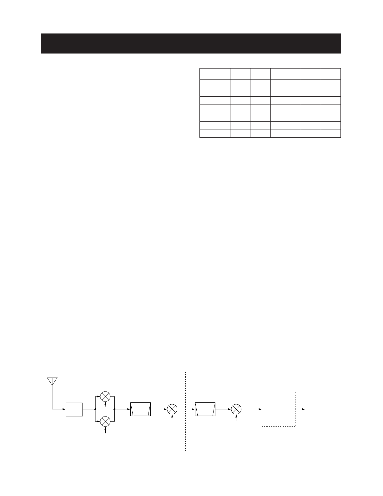
The level shifted signal is applied to the DSP IC (IC2001) for
36 kHz digital IF filter, demodulation, automatic notch and
noise reduction, etc. The output signal is level shifted 3.3 V
to 5V at the level converter (IC2052), and is applied to the
D/A converter (IC2351) to convert into the analog audio sig-
nals.
The converted audio signals are passed through the active
filter (IC2371a), AF amplifier (IC2371b), analog switches
(IC2372, pins 14, 13 and pins 1, 15) then applied to the low-
pass filter (IC2401). The filtered signals are passed through
the analog switches (IC2372, pins 4, 3 and IC2473, pins 1,
7), high-pass filter (IC2441A) and mixer amplifier (IC2471A),
and then applied to the MAIN-A unit via J2001 (pin 13) as
the DRAF signal.
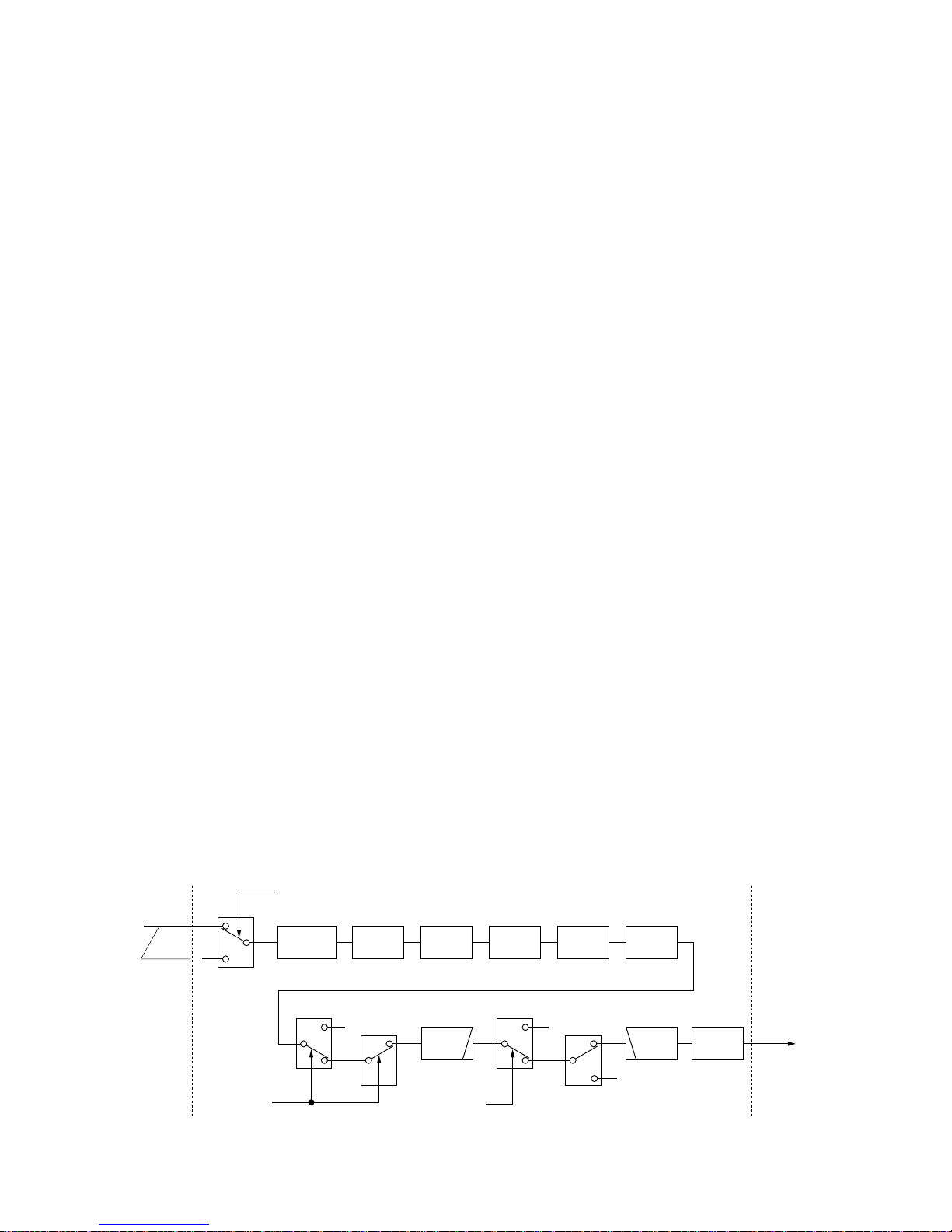
3-1-11 TWIN PBT CIRCUIT (DSP-A BOARD)
General PBT (Passband Tuning) circuit shifts the center fre-
quency of IF signal to electronically narrow the passband
width. The IC-756PRO™uses the DSP circuit for the digital
PBT function and actually shifts the both lower and higher
passbands of 3rd IF filter within ±1.8 kHz.
The twin PBT circuit in DSP IC (IC2001) controlled by the
[TWIN PBT] controller adjusts the 3rd IF passband width
and rejects interference.
3-1-12 AGC CIRCUIT (DSP-A BOARD)
The AGC (Automatic Gain Control) circuit reduces IF ampli-
fier gain and attenuates IF signal to keep the audio output at
a constant level.
The receiver gain is determined by the voltage on the AGC
line (IC2461, pin 4). The D/A converter for AGC (IC2461)
supplies control voltage to the AGC line and sets the receiv-
er gain with the [RF/SQL] control.
The 3rd IF signal from the level converter (IC2051) is detect-
ed at the AGC detector section in DSP IC (IC2001), and is
applied to the D/A converter for AGC via the level converter
(IC2052). TheAGC voltage is amplified at the buffer amplifi-
er (IC2471b) and is applied to the MAIN-A unit to control the
AGC line.
When receiving strong signals, the detected voltage increas-
es and the AGC voltage decreases via the buffer amplifier
(IC2471b). As the AGC voltage is used for the bias voltage
of the IF amplifier (RF-A unit; Q721), IF amplifier gain is
decreased.
3-1-13 S-METER CIRCUIT (MAIN-A UNIT)
The S-meter circuit indicates the relative received signal
strength while receiving by utilizing the AGC voltage which
changes depending on the received signal strength.
A portion of the AGC bias voltage from the DSP-A board is
applied to the differential amplifier (IC101a, pin 2) where the
difference between theAGC and reference voltage is detect-
ed.
The detected voltage is passed through the analog switch
(IC3631, pins 12, 14) as the SML signal and applied to the
main CPU (IC3501, pin 108) to activate the S/RF meter via
the sub CPU (IC401) on the DISPLAY board.
3-1-14 SQUELCH CIRCUIT (MAIN-A UNIT)
The squelch circuit mutes audio output when the S-meter
signal is lower than the [RF/SQL] setting level.
The S-meter signal is applied to the main CPU (IC3501, pin
108) and is compared with the threshold level set by the
[RF/SQL] control. The [RF/SQL] setting signal is applied to
the main CPU via the sub CPU (DISPLAY board; IC401, pin
91). The main CPU analyzes the compared signal and out-
puts control signal to the squelch gate (IC301, pin 5) via the
interface IC (IC3653, pin 19) to open or close the squelch as
the SQLS signal.
3-1-15 AF AMPLIFIER CIRCUIT (MAIN-A UNIT)
TheAF amplifier amplifies the audio signals to a suitable dri-
ving level for the speaker.
The AF signals (DRAF) from the DSP-A board are passed
through the squelch gate (IC301) and amplified at the AF
amplifier section of IC311 (pins 2, 4), and volume is con-
trolled by the AFGV signal at the VCA section (pins 7–9).
The volume controlledAF signals are passed through theAF
mute gate (IC331, pins 1, 7), then applied to the AF power
amplifier (IC332, pin 1) via the ripple filter (Q331).
The amplified audio signals are passed through the
[PHONES] and [EXT SP] jacks then applied to the internal
speaker when no plug is connected to the jacks.
The AF mute gate is controlled by the [AF] control via the
sub and main CPUs.
[PHONES]
[EXT SP]
Int. speaker
IC332
AF
power
amp.
DRAF
• AF amplifier circuit
7
61
IC301 IC311
Mute switchSquelch gate
Ripple
filter
Q331
MAIN-A unitDSP-A board
“SQLS” signal
“AFGV” signal
56
7
1
IC331 “AFMS” signal
2
AMP VCA

3 - 4
3-2 TRANSMITTER CIRCUITS
3-2-1 MICROPHONE AMPLIFIER CIRCUIT
(MAIN-A UNIT)
The microphone amplifier circuit amplifies microphone audio
signals to a level needed for the DSP circuit.
Audio signals from the [MIC] connector (MIC board; J1, pin
1) are amplified at the audio amplifier section in IC451 (pins
21, 22) via the analog switch (IC3002, pins 12, 14), then
applied to the buffer amplifier section (IC451, pin 5) and
VCA section. The gain controlled signals are output from
(IC451, pin 9) and passed through the analog switch
(IC3005, pins 14, 12) and then applied to the DSP circuit as
the DTAF signal.
The VCA section in IC451 (pins 7–9) controls microphone
input gain according to the [MIC GAIN] control level using
the MIGV signal coming from the main CPU via the I/O
expander (IC3751, pin 4).
3-2-2 VOX CIRCUIT (MAIN-A UNIT)
The VOX (Voice-Operated Transmission) circuit sets trans-
mitting conditions according to voice input.
A portion of the amplified audio signals from the AF amplifi-
er section in IC451 are again amplified at the VOX amplifier
section IC451 (pin 9), also gain contolloed signals at the
VCA section (pin 9) are amplified at the AF amplifier
(IC3004b, pins 6, 7), and then applied to the main CPU
(IC3501, pin 106) after passing through the analog switch
(IC362, pins 6, 1) as the VOXL signal.
The VOGV signal is applied to the VCA section in IC3003
(pin 7–9) from the main CPU via the I/O expander (IC3751,
pin 9) to adjust VOX actionable sensitivity. This is controlled
by the VOX gain set in the VOX SET mode.
3-2-3 DSP TRANSMITTER CIRCUIT
(DSP-A BOARD)
The microphone audio signals from the MAIN-A unit via the
DTAF line are applied to the analog switch (IC2201, pin 4)
and output from pin 3 or 5 to the each modulation circuits.
(1) When SSB mode
The audio signals from the analog switch (IC2201, pin 5) are
amplified at the limitter amplifier (IC2281b) and applied to
the low-pass filter (IC2281d/c) to limit the transmit passband
width.
The filtered signals are then applied to the differential ampli-
fiers (IC2301a/b) via the analog switch (IC2201) and T/R
switch (IC2291).
(2) When FM/AM modes
The audio signals from the analog switch (IC2201, pin 3) are
applied to the modulation adjustment pots (R2227: FM
mode, R2229: AM mode) via the limitter amplifier, pre-
emphasis circuit (only FM mode) and splatter filter consist of
IC2211. The level adjusted signals are applied to the differ-
ential amplifiers (IC2301a/b) after being passed through the
analog switch (IC2201) and T/R switch (IC2291). The pre-
emphasis circuit is cancelled by Q2201, Q2202, Q2211 on
AM mode.
The amplified signals at the differential amplifiers
(IC2301a/b) are applied to the A/D converter (IC2321). The
coverted signals are level shifted 5V to 3.3 V at the level
converter (IC2051).
The level shifted signal is applied to the DSP IC (IC2001)
and modulated at the DSP IC to produce the 36 kHz trans-
mitter IF signal. The modulated IF signal from the DSP IC is
level shifted 3.3 V to 5V at the level converter (IC2052), and
is applied to the D/A converter (IC2351) to convert into the
analog IF signal.
The converted IF signal is passed through the active filter
(IC2371a), buffer amplifier (IC2371b), analog switch
(IC2372, pins 14, 12) then applied to the low-pass filter
(IC2381d/c). The filtered signal is applied to the MAIN unit
via J2001 (pin 28) as the DTIF signal.
When SSB or RTTY mode, a portion of the filtered signal
from the low-pass filter (IC2381d/c) is amplified at the IF and
buffer amplifiers (IC2381b/c) and is applied to the transmit
monitor circuit for the monitor function.
3-2-4 SPEECH COMPRESSOR CIRCUIT
(DSP BOARD)
The speech compressor compresses the transmitter audio
input signals to increase the average output level (average
talk power).
When the speech compressor function is ON, the level shift-
ed signal from the level converter (IC2051) is applied to the
DSP IC (IC2001) and compressed at the DSP IC to obtain
an average audio level.
At the same time, the compressed signals are modulated at
the DSP IC and applied to the level converter (IC2052).
• Transmitter construction
1st LO
D771
Ceramic
filter
Crystal
filter
FI711
LPF BPFs
FI131
Ceramic
filter
FI133
MIC
Bandwidth
15 kHz
455 kHz
DSP-A
board
RF-A UNIT
MAIN-A UNIT
AMP VCA
FM/AM
modes
other
modes
3rd LO
(491 kHz)
IC221
64.455 kHz
2nd LO
(64.00 MHz)
D741
36 kHz IF
IC451 11
12
13
14
IC3005x
“MOSL” signal
DTAF DTIF

3 - 5
3-2-5 IF AMPLIFIER AND MIXER CIRCUITS
(MAIN-A AND RF-A UNITS)
The modulated 3rd IF signal from the DSP-A board (DTIF:
36 kHz) is applied to the 3rd mixer circuit (MAIN-A unit;
IC221, pin 1). The applied 3rd IF signal is mixed with the 3rd
LO signal from the DDS circuit (PLL unit; IC701) to produce
a 455 kHz 2nd IF signal.
The 2nd IF signal is output from pin 6 and amplified at the IF
amplifier (MAIN-A unit; Q241). The amplified signal is
passed through the ceramic bandpass filter (MAIN-A unit;
FI131: FM/AM modes, FI133: other modes) for unwanted
signals are suppressed. The filtered 2nd IF signal is amplli-
fied at IF amplifier (MAIN-A unit; Q261) and applied to the
2nd mixer circuit on the RF-A unit via J101.
The 2nd IF signal is mixed with the 64 MHz 2nd LO signal,
coming from the PLL unit, at the 2nd mixer circuit (RF-Aunit;
D741) to obtain a 64.455 MHz 1st IF signal. The 1st IF sig-
nal is passed through the MCFs (RF-Aunit; FI711a/b) to cut-
off the undesired signals then amplified at the IF amplifier
(RF-A unit; Q751) via the T/R switch (RF-A unit; D711). The
amplified 1st IF signal is applied to the 1st IF mixer circuit
(RF-A unit; D771).
The operating (transmitting) frequency is produced at the 1st
IF mixer circuit (RF-A unit; D771) by mixing the 1st IF and
1st LO signals. The mixed signal is then applied to the RF
circuit.
3-2-6 RF CIRCUIT (RF-A AND PA UNITS)
The RF circuit amplifies operating (transmitting) frequency
to obtain 100 W of RF output.
The signal from the 1st IF mixer is passed through the low-
pass filter (RF-A unit; L961, L962, C961–C965) and ampli-
fied at the RF amplifier (RF-Aunit; IC961). The amplified sig-
nal is again amplified at the wide-band YGR amplifier (RF-A
unit, IC151) after passing through one of 11 bandpass
(Refer to page 3-1 for bandpass filters used) and high-pass
filters, and is then applied to the PA unit via J151.
The signal applied from the RF-Aunit is amplified at the pre-
drive (Q1), drive (Q2, Q3) and power amplifiers (Q4, Q5) in
sequence to obtain a stable 100 W of RF output power. The
amplified signal is applied to one of 8 low-pass filters in the
FILTER unit.
3-2-7 LOW-PASS FILTER CIRCUIT (FILTER UNIT)
The low-pass filter circuit contains 8 Chebyschev low-pass
filters to suppress the higher harmonic components.
The signal from the power amplifiers on the PA unit is
applied to one of 8 low-pass filters, which is selected by the
I/O expander (IC11) in the CTRL unit via the buffer amplifier
(CTRL unit; IC12).
The filtered signal is then applied to one of 2 antenna con-
nectors via the CTRL only/and TUNER unit/s.
3-2-8 ALC CIRCUIT (MAIN-A UNIT)
The ALC (Automatic Level Control) circuit controls the gain
of IF amplifiers in order for the transceiver to output a con-
stant RF power set by the [RF POWER] control even when
the supplied voltage shifts, and etc.
The RF power level is detected at one of the APC detector
circuits (CTRL unit; D2) to be converted into DC voltage and
applied to the MAIN-A unit as the FORV signal.
The FORV signal from the CTRL unit is applied to the com-
parator (IC551b, pin 6). The POCV signal, controlled by the
[RF POWER] control via the I/O expander (IC3751, pin 5), is
also applied to the other input (pin 5) for reference. The
compared signal is output from pin 7 and applied to the IF
amplifiers in the MAIN-A (Q261) and RF-A (Q751) units to
control amplifying gain.
When the FORV signal exceeds the POCV voltage, ALC
bias voltage from the comparator controls the IF amplifiers.
This adjusts the output power to a specified level from the
[RF POWER] control until the FORV and POCV voltages are
equalized.
In AM mode, the comparator operates as an averaging ALC
amplifier. Q502 turns ON and the POCV voltage is shifted
for 40 W AM output power (maximum) through R510.
DTAF
• DSPTransmitter circuit
LPF
IC2281c/dIC2281b
IC2211a
LPF
IC2211b
MAIN-A unit DSP-A board
AF
signal
“MODS” signal
4
95
3
IC2201z
Mode switch
Differential
converter
A/D
converter DTIF
6
71
IC2291 IC2301a/b
IC2321 Level
converter
IC2051 D/A
converter
IC2052
Level
converter
IC2351
DSP IC
IC2001
LPF
IC2381d/c
T/R switch
13
12
14
IC2372x
MAIN-A unit
36 kHz IF
“TXS” signal
“TXS” signal
5
12
13 14
IC2201x
Mode switch
11
11
Limitter
Limitter
SSB
mode
FM/AM
mode

3 - 6
TheALC bias voltage is also applied to theALC meter ampli-
fier (IC551a, pin 2) to obtain an ALC meter signal (ALCL).
The amplified signal is passed through the analog switch (IC
3631, pins 13, 14) and applied to the main CPU (IC3501, pin
108) to drive the S/RF meter via the sub CPU (IC401) on the
DISPLAY board.
An external ALC input from the [ALC] jack or [ACC] sockets
is applied to the buffer amplifier (Q521). External ALC oper-
ation is identical to that of the internal ALC.
The FORV signal is also applied to the power meter amplifi-
er (IC571a, pin 3). The amplified signal is passed through
the analog switch (IC3631, pins 1, 15) as an FORL signal
and applied to the main CPU (IC3501, pin 109) to drive the
S/RF meter when the power meter is selected.
3-2-9 APC CIRCUIT (MAIN-A UNIT)
The APC (Automatic Power Control) circuit protects the
power amplifiers on the PA unit from high SWR and exces-
sive current.
The reflected wave signal appears and increases when the
connected antenna is mismatched to 50 Ω. The APC detec-
tor circuit (CTRL unit; D1 and L1) detects the reflected sig-
nal, and applies it to the APC circuit (IC551c, pin 9) as a
REFV signal.
When the REFV signal level increases, the APC circuit
decreases the ALC voltage to activate the APC.
For the currentAPC, the power transistor current is obtained
by detecting the voltages (ICH and ICL) which appear at
both terminals of the current detector (PA unit; R28). The
detected voltages are applied to the differential amplifier
(IC551d, pins 12, 13). When the current of transistors is
increased, the amplifier controls the ALC line to prevent
excessive current flow.
A portion of the REFV signal is applied to the SWR meter
amplifier (IC571b, pin 5). The amplified signal is passed
through the analog switch (IC3631, pins 3, 4) as an REFL
signal and applied to the main CPU (IC3501, pin 110) to
drive the S/RF meter when the SWR meter is selected.
3-2-10 TEMPERATURE PROTECTION CIRCUIT
(PA UNIT)
The cooling fan (CHASSIS; MF1) is activated while trans-
mitting or when the temperature of the power amplifier
exceeds the preset value. The temperature protection circuit
consists of Q10–Q13 and R50.
While transmitting, Q10 and Q12 are turned ON, and pro-
vide a voltage to the cooling fan to rotate at medium speed.
The thermistor (R50) detects the temperature of the final
amplifier (Q5), and activates Q11 and Q13 to accelerate the
cooling fan when the detected temperature exceeds 70˚C
(158˚F). The cooling fan rotates at high speed at 80˚C
(176˚F) or more.
The thermistor keeps the cooling fan rotating even while
receiving until the Q5 temperature drops to 60˚C (140˚F) or
below.
3-2-11 MONITOR CIRCUIT
(DSP-A BOARD AND MAIN-A UNIT)
The microphone audio signals can be monitored to check
voice characteristics.
(1) When FM/AM modes (MAIN-A UNIT)
Aportion of the microphone audio signals from the VCAsec-
tion in IC451 are applied to the analog switch (IC361). The
selected audio signals are applied to IC371 (pin 2), and the
output signals from pin 9 are applied to the AF amplifier cir-
cuit (IC311, pin 7).
(2) When SSB/RTTY modes
(DSP-A BOARD)
A portion of the transmit IF signal from the low-pass filter
(IC2381d/c) is amplified at the IF (IC2381b) and buffer
(IC2381a) amplifiers, and applied to the digital mixer circuit
(IC2302). The applied signal is mixed with a 36 kHz LO sig-
nal from the D/A converter (IC2342) to demodulate into the
AF signals. The demodulated signals are passed through
the buffer amplifier (IC2381a), low-pass filter (IC2441b/c)
and AF amplifier (IC2441d), and then applied to the MAIN-A
unit as the DMAF signal.
The DMAF signal from the DSP-A board is amplified at the
ALC amplifier (MAIN-A unit; IC372, pins 13, 1) and applied
to the VCA section of IC371 (MAIN-A unit; pins 7, 9). The
volume controlled AF signals is applied to the AF amplifier
circuit (MAIN-A unit; IC311, pin 7).
3-3 PLL CIRCUITS
3-3-1 GENERAL
The PLL unit generates a pair of 1st LO frequencies
(64.485–124.455 MHz) for dualwatch and spectrum scope
functions; a 2nd LO frequency (64 MHz), 3rd LO frequency
(491 kHz) and sweep LO frequency for the spectrum scope
function.
The 1st LO PLLs adopt a mixer-less dual loop PLL system
and has 4 VCO circuits. The LOs, except the 2nd, use DDSs
while the 2nd LO uses the fixed frequency of the crystal
oscillator.
3-3-2 1ST LO PLL CIRCUIT
The 1st LO PLLs contain a main and reference loop as a
dual loop system. Both PLLs have equivalent circuits— this
manual describes only the 1st LO PLL A circuit.
The reference loop generates a 10.747 to 10.865 MHz fre-
quency using a DDS circuit, and the main loop generates a
64.485 to 124.455 MHz frequency using the reference loop
frequency.
(1) REFERENCE LOOP PLL
The oscillated signal at the reference VCO (Q151, D151) is
amplified at the buffer amplifiers (Q152, Q102) and is then
applied to the DDS IC (IC101, pin 46). The signal is then
divided and detected on phase with the DDS generated fre-
quency.
The detected signal output from the DDS IC (pin 56) is con-
verted into DC voltage (lock voltage) at the loop filter
(R135–R137, C121, C151) and then fed back to the refer-
ence VCO circuit (Q151, D151).

3 - 7
(2) MAIN LOOP PLL
The oscillated signal at one of the main loop VCOs (Q201,
D201, D202), (Q221, D221, D222), (Q251, D251–D254) and
(Q271, D271–D274) is amplified at the buffer amplifiers
(Q301, IC320) and is then applied to the PLL IC (IC381, pin
6) via the low-pass filter (L303, C304–C307). The signal is
then divided and detected on phase with the reference loop
output frequency.
The detected signal output from the PLL IC (pin 2) is con-
verted into a DC voltage (lock voltage) at the loop filter and
then fed back to one of the VCO circuits (Q201, D201,
D202), (Q221, D221, D222), (Q251, D251–D254) and
(Q271, D271–D274).
The oscillated signal is amplified at the buffer amplifiers
(Q301, IC320) and then applied to the RF-Aunit as a 1st LO
A signal after being passed through the low-pass filters
(L303, C304–C307 and L351–L353, C351–C356) and high-
pass filter (L354, C358–C360) and mute circuit (D361).
3-3-3 2ND LO AND REFERENCE OSCILLATOR
CIRCUITS
The reference oscillator (X52, Q51) generates a 32.00056
MHz frequency for the 4 DDS circuits as a system clock and
for the LO output. The oscillated signal is doubled at the
doubler circuit (Q71, Q81) and the 64.0 MHz frequency is
picked up at the double tuned filter (L81, L82). The 64.0
MHz signal is applied to the RF-A unit as a 2nd LO signal.
3-3-4 3RD LO CIRCUIT
The DDS IC (IC701) generates a 10-bit digital signal using
the 32 MHz system clock. The digital signal is converted into
an analog wave signal at the D/A converter (R701–R720).
The converted analog wave is passed through the bandpass
filter (L702, L703, C709–C713) and then applied to the
MAIN-A unit as the 3rd LO signal.
3-3-5 MARKER CIRCUIT
The divided signal at the DDS circuit (IC101) is used for the
marker signals with the IC-756PRO™.
The reference signal for the DDS circuit (32.0 MHz) is divid-
ed to produce an acceptable frequency signal, 16 MHz, with
the programmable divider then divided again by 160 to
obtain 100 kHz cycle square-wave signals.
The generated marker signals are output from pin 66 of the
DDS IC (IC101), and are then applied to the RF unit via the
mute switch (IC192) and J851 as the MKR signal.
• PLL CIRCUIT
64.485–
124.455 MHz
10.747–
10.865 MHz
64.485–
124.455 MHz
64.0 MHz
77.8 MHz
ANT
1st mixer A
Q511–Q514
491 kHz
to scope circuit
(RF-A unit, D831)
to scope circuit
(RF-A unit, IC841)
IC801IC701
IC101
IC381
IC901
Q71
Q81
Q902
S2LOS3LO
3LO2LO
1LOB
1LOA
77.8 MHz
RF-A unit
PLL unit
MAIN-A unit
Q201
Q221
Q251
Q271
Q151
1st LO PLL A
circuit
Phase
detector
1/N divider
1/22
Phase
detector
12 bit
D/A
Main loop PLL
Ref. loop PLL
DDS
1st mixer B
1st LO
PLL B
circuit
✕2
DDS
D/A
DDS
D/A
PLL
IC
Crystal
filter
2nd mixer
D941 3rd mixer
IC151
64.455 MHz
to DSP-A board
Reference oscillator
X52: 32.0 MHz
BPFBPF
Loop
filter
LPF
LPF

3 - 8
3-4 ANTENNA TUNER CIRCUITS
3-4-1 MATCHING CIRCUIT (TUNER UNIT)
The matching circuit is a T-network. Using 2 tuning motors,
the matching circuit obtains rapid overall tuning speed.
Using relays (RL1–RL15), the relay control signals from the
antenna tuner CPU (CTRL unit; IC5) via the buffer amplifier
(IC1, IC2) ground one of the taps of L3–L12 and add capac-
itors (C27–C43). After selecting the coils and capacitors, 2
motors (CTRL unit; MF1, MF2) adjust C44 and C45 using
the antenna tuner CPU (CTRL unit; IC5) and the motor con-
troller (CTRL unit; Q211–Q218, D211, D213, D215, D217) to
obtain a low SWR (Standing Wave Ratio).
3-4-2 DETECTOR CIRCUIT (CTRL UNIT)
(1) SWR detector
Forward and reflected power are picked up by a current
transformer (L1), detected by D2 and D1, and then amplified
at IC1a and IC1b, respectively. The amplified voltages are
applied to the antenna tuner CPU (IC5, pins 2, 3). The tuner
CPU detects the SWR.
(2) Reactance components detector
Reactance components are picked up by comparing the
phases of the RF current and RF voltage. The RF current is
detected by L4 and R16 and buffer-amplified at IC14e and
IC2a and then applied to the phase comparator (IC3a). RF
voltages are detected by C12–C14 and then applied to the
phase comparator (IC3b) after being amplified at the buffer
amplifiers (IC14c, IC2b). The output signal from the phase
comparator (IC3a, pin 6 for RF current, IC3b pin 7 for RF
voltage) is rectified at D7 and D6 for conversion into DC volt-
age. The rectified voltage signals are combined, then ampli-
fied at the inverter amplifier (IC4b), then applied to the
antenna tuner CPU (IC5, pin 64).
A C-MOS IC is used for the buffer amplifier (IC14) to
improve functionable sensitivity; the inverter amplifier (IC4)
is very responsive even with a low signal level input.
Together, these ensure quick and stable signal detection
even at low RF signal level input.
(3) Resistance components detector
Resistance components are picked up by L8, and detected
by D8, D9 and Q5. The detected resistance components are
amplified at the inverter amplifier (IC4a), and then applied to
the antenna tuner CPU (IC5, pin 1).
3-4-3 MOTOR CONTROL CIRCUIT
(CTRL AND TUNER UNITS)
The control circuit of the internal antenna tuner consists of
the CPU, EEPROM (Electronically-Erasable Programmable
Read Only Memory), tuning motors and tuning relays.
(1) CPU and EEPROM (CTRL unit)
The antenna tuner CPU (IC5) controls the tuning motors via
the motor controller (Q211–Q218, D211, D213, D215, D217)
and tuning relays, and memorizes the best preset position in
100 kHz steps. The memory contents are stored in the EEP-
ROM (IC6) without a backup battery.
(2) Tuning motors (CTRL and TUNER units)
A motor controller (Q211–Q218, D211, D213, D215, D217)
rotates the tuning motors (TUNER unit; MF1, MF2) to obtain
a low SWR.
(3) Tuning relays (TUNER unit)
According to the operating frequency band and antenna
condition, tuning relays select the capacitors and coils.
3-4-4 ANTENNA TUNER CPU PORT ALLOCATION
(CTRL unit; IC5)
1
2
3
4
6
7
13
15
17
21
22, 23
26
27–32
34–40
41–48
64
Input port for the resistance com-
ponents detection voltage.
Input port for the reflected RF
power voltage.
Inpout port for the forward RF
power voltage.
Input port for the transceiver power
OFF.
Inputs low level signal when oper-
ating the antenna tuner in 50 MHz
band.
Input port for reference voltage set-
ting.
Outputs tuner data signal.
Input port for the serial signal.
Input port for the [TUNER]
ON/OFF signal.
Input port for the TX/RX switching
signal.
Input port for the antenna tunner
CPU system clock.
Outputs the coil selection signal.
High : While 46–60 MHz band is
displayed.
Output the coil selection signal.
Output the capacitor selection sig-
nal.
Output pulse-type control signals
for the tuning motors (MF1, MF2).
Input port for the reactance compo-
nents detection voltage.
R
REF
FOR
PWRS
STDU
SETI
KEY
START
THRU
SEND
CL1, CL2
DUAL
L24M, L18M,
L14M, L10M,
L7M, L3.5M
CO3, CO2,
CO1, CI3,
CI2, CI1
PZ, PY, PX,
PW, RZ, RY,
RX, RW
P
Pin Port Description
number name

3 - 9
3-5 SCOPE CIRCUITS
3-5-1 SCOPE RECEIVER CIRCUIT (RF-A UNIT)
A portion of the 64.455 MHz 1st IF signal from the 1st mixer
circuit (Q511–Q514: while receiving) or IF amplifier (Q751:
while transmitting) is passed through the PIN attenuator
(D801) and amplified at the IF amplifiers (Q811, Q812), and
then mixed with the 77.8 MHz scope 2nd LO (S2LO) signal
at the mixer circuit (D831) to produce the 13.345 MHz IF sig-
nal. The mixed IF signal is passed through the ceramic
bandpass filters (FI843, FI841) to suppress unwanted sig-
nals. The filtered IF signal is applied to the FM IF IC (IC841,
pin 16).
The applied 13.345 MHz IF signal is mixed with the sweep
LO (S3LO) signals from the PLLunit at the FM IF IC (IC841),
which includes the RSSI terminal. The mixed IF signals are
filtered at the ceramic bandpass filter (FI842) then applied to
the limiter amplifier section in the FM IF IC (IC841, pin 5).
The applied IF signals are converted into DC voltages
according to the applied IF signal strength at the RSSI sec-
tion in the IC.
The converted voltages are output from pin12 (IC841) and
amplified at IC871b, then applied to the MAIN-A unit as the
SCPL signal.
Some of the DC voltages from the FM IF IC (IC841) are
amplified at IC871a to produce AGC voltages for the IF
amplifiers (Q811, Q812), producing wider dynamic range.
By sweeping LO signals (S3LO) are applied to the mixer
section in the FM IF IC (IC841), the spectrum scope function
is activated.
3-5-2 SWEEP LO CIRCUIT (PLL UNIT)
The sweep LO signals (S3LO) are generated by the DDS IC
(IC801) using the 32 MHz system clock. A 10-bit digital sig-
nal is converted into analog wave signals at the D/A con-
verter (R801–R820). The converted analog wave is passed
through the bandpass filter (L802, L803, C809–C813) then
applied to the RF-A unit after being amplified at the buffer
amplifier (Q802).
3-6 POWER SUPPLY CIRCUITS
3-6-1 PA UNIT
3-6-2 FRONT UNIT
• SCOPE CIRCUIT DIAGRAM
RF-A unit
1st mixer A
Q511–Q514
Q811
to 2nd mixer circuit
to the MAIN-A unit SCPL signal
Q812
D831 FI843 FI841
Ceramic
BPF Ceramic
BPF
IF
amp.
IC871a
AGC
IC871b
amp.
IF
amp.
Ceramic
BPF
Limiter
amp.
Mixer
IC841
FI842
S3LO signal
(12.79–12.99 MHz*)
S2LO signal
(77.80 MHz)
1st LO
signal
16
12
5
3
2
RSSI
*depending on sweeping passband width
RF signals
LINE
PHV
HV
14V
14VA
8V
5V
H5V
DESCRIPTION
The voltage from an external power supply via
the common filter circuit (FILTER unit; L501,
L502).
The same voltage as the PHV line passed
through a fuse (F1).
The same voltage as the HV line passed through
the switching relay (RL1).
The same voltage as the 14 V line is applied to
the AF power amplifier (MAIN-A unit; IC332).
Common 8 V converted from the 14 V line and
regulated by the +8 regulator circuit (IC3).
Common 5 V converted from the 14 V line and
regulated by the +5 regulator circuit (IC2).
Common 5 V converted from the HV line and
regulated by the H5V regulator circuit (IC1).
LINE
5VF
–15V
–7V
–8V
+18V
DESCRIPTION
Common 5 V converted from the 14 V line and
regulated by the +5 regulator circuit (IC861).
Common –15 V converted from the 14 V line and
converted by the –15 DC-DC converter circuit
(IC841, Q841, D841). The voltage is applied to
the –7 V, –8 V regulator circuits and etc.
Common –7 V converted from the –15 V line and
regulated by the –7 regulator circuit (IC501).
Common –8 V converted from the –15 V line and
regulated by the –8V regulator circuit (IC881).
Common 18 V converted from the 14 V line and
converted by the 18 V DC-DC converter circuit
(IC821, Q821, D822).

3 - 10
3-6-3 MAIN-A UNIT
3-6-4 CTRL AND PLL UNITS
3-7 LOGIC CIRCUITS
3-7-1 BAND SELECTION DATA
(RF-A, CTRL AND PLL UNITS)
To select the correct bandpass, low-pass filters and VCOs
on the RF-A, FILTER and PLL units, the main CPU (MAIN-
A unit, IC3501) outputs the following band selection data via
the I/O expander (RF-Aunit, IC901, IC902, CTRL unit, IC11)
or DDS IC (PLL unit, IC101, IC401) depending on the dis-
played frequency.
The D/A convertor (MAIN-A unit, IC3751) output signal from
pin 7 is amplified at IC101b (pins 5–7) to obtain the band volt-
age for external equipment via the [ACC 2] connector pin 4.
3-7-2 SUB-CPU PORT ALLOCATIONS
(DISPLAY BOARD; IC401)
0.003–1.599999
1.6–1.999999
2.0–2.999999
3.0–3.999999
4.0–5.999999
6.0–7.999999
8.0–10.999999
11.0–14.999999
15.0–19.999999
20.0–21.999999
22.0–29.999999
30.0–44.999999
45.0–49.999999
50.0–54.000000
54.000001–
60.000000
Frequency
IC901, IC902
IC11 IC101 IC401
[MHz]
(RF-A unit)
(CTRL) (PLL) (PLL)
BPF LPF VCO-A VCO-B
B0
B1
B2
B3
B4
B5
B6
B7
B8
B9
B10W
B10
B10W
L1S
L2S
L3S
L4S
L5S
L6S
L7
VA1S
VA2S
VA3S
VA4S
VB1S
VB2S
VB3S
VB4S
LINE
R8V
T8V
DESCRIPTION
Receive 8 V converted from the 14 V line and
regulated by the R8V regulator circuit (Q601,
Q602, D601).
Transmit 8 V converted from the 14 V line and
regulated by the T8V regulator circuit (Q611,
Q612, D611).
LINE
5V
5V
DESCRIPTION
Common 5 V for the antenna tuner CPU (CTRL
unit; IC5) and the EEPROM (CTRL unit; IC6),
converted from the 14 V line and regulated by
the +5 regulator circuit (CTRL unit; IC13).
Common 5 V for each PLL-A and PLL-B circuits
regulated from the 8 V line and regulated by the
+5 regulator circuit (PLL unit; IC382: PLL-A,
IC682: PLL-B).
7, 8
9
12, 83
56, 57
64–66
67–75
77, 79
81
82, 84
85, 88
86
87
92
93
94
95
96
97
98
99
100
Input and output ports for the system
clock oscillator (X401; 9.8304 MHz).
Input port for the reset signal.
Input port for the [DIAL]; pulse-type
signals are applied.
Input ports for the [ELEC-KEY] jack.
Output ports for the S/RF meter back-
light and function switch activation
indicator brightness control signal.
Control signal output ports for the acti-
vation indicator of function switches.
High: When the function is activated.
Input port for the [TWIN PBT (inner)]
control (PBT board, S1/inner).
Outputs the S/RF meter (ME1) drive
signal.
Input ports for the [RIT/∆TX] control;
pulse-type signals are applied.
Input port for the [TWIN PBT(outer)]
control (PBT board, S1/outer).
Input port for data signal from the
main-CPU (MAIN unit; IC3501).
Outputs data signal for the main-CPU
(MAIN unit; IC3501).
A/D input port for the [BAL] control
(R702/ inner).
A/D input port for the [NR] control
(R702/ outer).
A/D input port for the [MIC GAIN] con-
trol (R712).
Input port for the [RF POWER] control
(R714).
Input port for the [COMP] control
(R716).
Input port for the [KEY SPEED] control
(R718).
Input port for the [BK-IN DELAY] con-
trol (R720).
Input port for the [NOTCH] control
(PBT board, R1/inner).
Input port for the [CW PITCH] control
(PBT board, R1/outer).
OSC1,
OSC2
DRES
MSB,
MSA
DOTK,
DSHK
MDM0–
MDM2
TNRD, MOND
NBD, NRD
LOCD, TXD
RXD, PBTD
NOTD
PB1B,
PB1A
METV
RSA,
RSB
PB2A,
PB2B
LMFD
LFMD
BALL
NRL
MIGL
PWRL
CMPL
KYSL
DELL
NOTL
PITL
Pin Port Description
number name
Backlight level
Port 1234567
MDM0
MDM1
MDM2
High High High High HighLow Low Low
Low High
High High High High
Low High HighLow
Low Low Low

3 - 11
3-7-3 MAIN-CPU PORT ALLOCATIONS
(MAIN UNIT; IC3501)
6–9,
11–18,
20–26
29
30
31
32
34
37
40–43,
45–52,
54–57
59
61
63
64
66
69
70
71
72
73
74
75
76
77
Address signal output ports for the
LCD controller (IC3551).
Input port for the [KEY] jack.
Low : During key down
Input port for the RTTY keying.
Power supply detection input port for
the DSP-A board.
Input port for data signal from DSP-A
board.
Input port for the [POWER] switch.
Low : When the [POWER] is pushed.
Outputs CW/RTTY keying.
Data bus lines for the LCD controller
(IC3551) and I/O expander
(IC3652–IC3654).
Output port for the CI-V signal.
Input port for the CI-V signal.
Outputs clock signal.
Outputs data signal.
Input port for the [XVERT] detection
signal.
Input port for transmit control signal
from the antenna tuner CPU (CTRL
board; IC5).
Outputs R8V regulator (Q601, Q602,
D601) control signal.
Low : While receiving
Outputs T8V regulator (Q611, Q612,
D611) control signal.
Low : While transmitting
Outputs antenna tuner start signal.
Outputs reset/inhibit signal to the sub-
CPU (DISPLAY board; IC401), DDS
ICs (PLL unit; IC101, IC401), antenna
tuner CPU (CTRLboard; IC5), and etc.
Input port for unlock signal from the
PLL unit.
Outputs strobe signals for the I/O
expander IC (PLL unit; IC1).
Outputs strobe selection signals for
the I/O expander (PLL unit; IC1).
Outputs control signal for the DDS cir-
cuits (PLL unit; IC101, IC401).
A0–A3,
A4–A11,
A12–A18
SKYS
RTKI
DPGI
DSDR
PWRK
DSKY
DB0–DB3,
DB4–DB11,
DB12–DB15
CTXD
CRXD
MCK
MDAT
TRVI
IKEY
RXS
TXS
ISTA
DRES
UNLC
PSTB
PSEL
CON2
Pin Port Description
number name
78
79
85, 86
96
97
98
101
105
106
107
108
109
110
111
112
115
116
Outputs data signal for the DDS cir-
cuits (PLL unit; IC101, IC401).
Outputs clock signal for the DDS cir-
cuits (PLL unit, IC101, IC401).
Input ports for the CPU system clock
oscillator (X3501; 19.6608 MHz).
Outputs reset/inhibit signal for the LCD
controller (IC3551), I/O expander
(IC3652–IC3654), and etc.
Outputs data signal for the sub-CPU
(DISPLAY board; IC401).
Input port for data signal from the sub-
CPU (DISPLAY board; IC401).
Outputs [TIMER] indicator control sig-
nal.
High: When the timer function is ON
Input port for the scope signal.
A/D input port for the VOX gain.
A/D input port for the anti-VOX level.
A/D input port via the analog switch
(IC3631) for the SML signal from the
S-meter amplifier circuit (IC101a), and
ALCL signal from the ALC meter
amplifier circuit (IC551a).
A/D input port via the analog switch
(IC3631) for the NSQO signal from the
level conveter (DSP-A board; IC2063),
for noise squelch operation, and FORL
signal from the power meter amplifier
circuit (IC571a).
A/D input port from the analog switch
(IC3631) for the FNTL signal from the
low-pass filter (DSP-A board;
IC2472a), for tone squelch operation,
and REFL signal from the SWR meter
amplifier circuit (IC571b).
Outputs CW side-tone signals.
Outputs beep audio signals.
Input port for connected microphone’s
PTT switch and SEND signal from the
ACC jacks.
High: While PTT switch is pushed or
activated from an external unit.
Outputs control signal for the power
switching relay (PA unit; RL1) .
High: During power ON
CON1
(PDAT)
CON0
(PCK)
XTAL,
EXTAL
LRES
LTXD
LRXD
TMD
SCPL
VOXL
AVXL
ASO0
ASO1
ASO2
STON
BEEP
SENI
PWRS
Pin Port Description
number name

3-7-4 INPUT EXPANDER ALLOCATIONS
(1) DISPLAY board; IC411
(2) MAIN-A unit; IC3652
3-7-4 OUTPUT EXPANDER ALLOCATIONS
(1) PLL unit; IC1
(2) PLL unit; IC101
(3) PLL unit; IC401
3 - 12
1
5
12
13
14, 15
Input port for the [RIT], [∆TX] and
[CLEAR] switches.
Input port for [UP] and [DN] switches
of the connected microphone.
Input port for the [D-WATCH],
[CHANGE], [V/M] and [M/S] switches.
Input port for the [TUNER], [MONI-
TOR], [NB] and [NR] switches.
Input ports for the multi-function
switches.
KI4
MUDK
KI3
KI0
KI1, KI2
Pin Port Description
number name
11
12
13
14
16
17
18
Input port transmission status for CW
Input port for RTTY decode data.
Input port for the KEY signal from the
connected AH-3.
Low : While tuning or tune NG
Input port for AH-3 connection detec-
tion.
High: When AH-3 is connected.
Input port for interrupting signal
from audio recoder.
Input port for address clock signal
from audio recoder.
Input port for busy signal from the
installed UT-102 SPEECH SYNTHE-
SIZER.
CTFL
RTDT
EKEY
TCON
VINT
VRAC
SBSY
Pin Port Description
number name
66
68
70
71
73
74
75
Outputs the marker mute switch (IC192)
control signal.
High: When the [MARKER] is ON and
receiving.
Outputs LO mute switch (Q361) control
signal. Low : Muted
Outputs bandpass filter select switch
(Q351) control signal.
High: When less than 8 MHz is dis-
played on the main band.
Outputs the LO switch (Q121) control
signal.
High: While 45.0–60.0 MHz band is
displayed on the main band.
Outputs the LO switch (Q122) control
signal.
High: While 20.0–44.999999 MHz
band is displayed on the main
band.
Outputs the LO switch (Q123) control
signal.
High: While 8.0–19.999999 MHz band
is displayed on the main band.
Outputs the LO switch (Q126) control
signal.
High: While 0.03–7.999999 MHz band
is displayed on the main band.
MAKS
PAMT
PAFS
VA4S
VA3S
VA2S
VA1S
Pin Port Description
number name
68
70
71
73
74
75
Outputs LO mute switch (Q661) control
signal. Low : Muted
Outputs bandpass filter select switch
(Q651) control signal.
High: When less than 8 MHz is dis-
played on the main band.
Outputs the LO switch (Q421) control
signal.
High: While 45.0–60.0 MHz band is
displayed on the main band.
Outputs the LO switch (Q422) control
signal.
High: While 20.0–44.999999 MHz
band is displayed on the main
band.
Outputs the LO switch (Q423) control
signal.
High: While 8.0–19.999999 MHz band
is displayed on the main band.
Outputs the LO switch (Q426) control
signal.
High: While 0.03–7.999999 MHz band
is displayed on the main band.
PBMT
PBFS
VB4S
VB3S
VB2S
VB1S
Pin Port Description
number name
4
5
6
7
12
13
14
Outputs strobe signals to DDS IC
(IC101) for the 1st LO PLL A circuit.
Outputs strobe signals to PLL IC
(IC381) for the 1st LO PLL A circuit.
Outputs strobe signals to DDS IC
(IC401) for the 1st LO PLL B circuit.
Outputs strobe signals to PLL IC
(IC681) for the 1st LO PLL B circuit.
Outputs strobe signals to DDS IC
(IC701) for the 3rd LO PLL circuit.
Outputs strobe signals to PLL IC
(IC901) for the S2 LO PLL circuit.
Outputs strobe signals to DDS IC
(IC801) for the S3 LO PLL circuit.
PST1
PST2
PST3
PST4
PST5
PST6
PST7
Pin Port Description
number name

3 - 13
(4) CTRL board; IC11
(5) RF-A unit; IC901
(6) RF-A unit; IC902
(7) RF-A unit; IC905
4
5
6
7
11
12
13
14
Outputs a low-pass filter select signal.
High: When 0.03–1.999999 MHz
band is selected.
Outputs a low-pass filter select signal.
High: When 2.0–5.999999 MHz band
is selected.
Outputs a low-pass filter select signal.
High: When 6.0–7.999999 MHz band
is selected.
Outputs a low-pass filter select signal.
High: When 8.0–11.999999 MHz
band is selected.
Outputs a low-pass filter select signal.
High: When 30.0–60.0 MHz band is
selected.
Outputs a low-pass filter select signal.
High: When 22.0–29.999999 MHz
band is selected.
Outputs a low-pass filter select signal.
High: When 15.0–21.999999 MHz
band is selected.
Outputs a low-pass filter select signal.
High: When 12.0–14.999999 MHz
band is selected.
L1S
L2S
L3S
L4S
L8S
L7S
L6S
L5S
Pin Port Description
number name
4
5
6
7
11
12
13
14
Outputs a bandpass filter select signal.
High: When 0.03–1.599999 MHz
band is selected.
Outputs a bandpass filter select signal.
High: When 1.6–1.999999 MHz band
is selected.
Outputs a bandpass filter select signal.
High: When 2.0–2.999999 MHz band
is selected.
Outputs a bandpass filter select signal.
High: When 3.0–3.999999 MHz band
is selected.
Outputs a bandpass filter select signal.
High: When 8.0–10.999999 MHz
band is selected.
Outputs a bandpass filter select signal.
High: When 7.0–7.299999 MHz band
is selected.
Outputs a bandpass filter select signal.
High: When 6.0–6.999999 MHz or 7.3–
7.999999 MHz band is selected.
Outputs a bandpass filter select signal.
High: When 4.0–5.999999 MHz band
is selected.
B0S
B1S
B2S
B3S
B6S
B5S
B5WS
B4S
Pin Port Description
number name
4
5
6
7
12
13
14
Outputs a low-pass filter select signal.
High: When 11–13.999999 MHz or
14.5–14.999999 MHz band is
selected.
Outputs a low-pass filter select signal.
High: When 14.0–14.499999 MHz
band is selected.
Outputs a low-pass filter select signal.
High: When 15.0–20.999999 MHz or
21.5–21.999999 MHz band is
selected.
Outputs a low-pass filter select signal.
High: When 21.0–21.499999 MHz
band is selected.
Outputs a low-pass filter select signal.
High: When 50.0–54.0 MHz band is
selected.
Outputs a low-pass filter select signal.
High: When 30.0–49.999999 MHz or
54.000001–60.0 MHz band is
selected.
Outputs a low-pass filter select signal.
High: When 22.0–29.999999 MHz
band is selected.
B7WS
B7S
B8WS
B8W
B10S
B10WS
B9S
Pin Port Description
number name
4
5
6
7
14
Outputs control signal for the attenua-
tor circuit (RL121, R121, R122).
Low : When 6 dB attenuator is ON
Outputs control signal for the attenua-
tor circuit (RL122, R123, R124).
Low : When 12 dB attenuator is ON
Outputs control signal for the pre-
amplifier 1 circuit (Q441, Q442).
High: When P.AMP 1 is selected.
Outputs control signal for the pre-
amplifier 2 circuit (IC451).
High: When P.AMP 2 is selected.
Outputs the RX antenna select signal.
Low : When [RX ANT] is selected.
AT1S
AT2S
PR1S
PR2S
RANS
Pin Port Description
number name

3 - 14
(8) MAIN-A unit; IC3653
(9) MAIN-A unit; IC3654
(10) MAIN-A unit; IC3752
(11) MAIN-A unit; IC3753
13
14
15
16
17
18
19
Outputs strobe signals for the output
expander ICs (RF-A unit; IC901,
IC902, IC905).
Outputs the antenna connector
([ANT1] or [ANT2]) select signal.
High: When the [ANT2] is selected.
Outputs strobe signals for the output
expander (CTRL board; IC11).
Outputs strobe signals for the D/Acon-
verter (IC3751).
Outputs strobe signals for the output
expander ICs (IC3752, IC3753).
Outputs control signal for the AF mute
switch (IC331).
High: When the [AF] control is set to
maximum counter clockwidth.
Outputs squelch mute control signal,
applied to the squelch gate (IC301).
High: Squelched
BSTB
ANTS
FSTB
ASTB
MSTB
AFMS
SQLS
Pin Port Description
number name
12
13
14
15
16
17, 18
Outputs squelch control signal for the
[MIC] and [ACC1] connectores.
High: Squlch opend. (RX LED ON)
Outputs control signal for the internal
speaker ON/OFF select relay (RL351).
High: Internal speaker is ON.
Outputs strobe signals for the optional
UT-102 SPEECH SYNTHESIZER.
Outputs chip select signal for the audio
recoder (IC3001).
Outputs external antenna tuner (AH-3)
start signal.
Low : When the [TUNE] switch is
pushed.
Outputs control signal for the DSP IC
(DSP-A board; IC2001).
SQSS
SPS
SSTB
VCS
ESTA
DSFR,
DSFW
Pin Port Description
number name
4
6
7
12
14
Outputs control signal for the noise
blanker switch (Q3751, Q3752).
High: When the [NB] switch is ON,
except in FM mode.
Outputs audio select signal for the TX
monitor function.
High: During monitoring in SSB or
RTTY mode.
Outputs audio select signal for the TX
monitor function.
High: During monitoring in AM or FM
mode.
Outputs analog switch (IC3005) con-
trol signal for the audio recoder’s
(IC3001) output.
High: When the audio recoder’s out-
put to the AF circuit.
Outputs analog switch (IC3002) con-
trol signal for input of the microphone
amplifier (IC461).
High: Except the microphone input is
selected.
NBS
MSL1
MSL2
VOSL
MISL
Pin Port Description
number name
4
5
6
7
11
14
Outputs AM mode select signal for the
AGC and APC circuit.
High: When AM is selected.
Outputs HF band RF power control
signal.
High: When 0.03–29.999999 MHz
band is selected.
Outputs 50 MHz band RF power con-
trol signal.
High: When 30–60 MHz band is
selected.
Outputs 2nd IF filter (FI131 or FI133)
select signal.
High: When transmitting in AM or FM
mode. (FI131 is ON)
Outputs reset signal for the DSP circuit
and etc.
Outputs FM deviation control signal.
High: When FM-N is selected.
AMS
PHFS
P50S
MODS
DSRS
FMNS
Pin Port Description
number name
Other manuals for IC-756PROII
2
Table of contents
Other Icom Transceiver manuals

Icom
Icom IC-F9020 SERIES User manual

Icom
Icom IC-22U User manual

Icom
Icom IC-F70DS User manual

Icom
Icom IC-F1100D Series User manual

Icom
Icom IC-V101 User manual

Icom
Icom ID-51A Setup guide

Icom
Icom IC-F8100 User manual

Icom
Icom IC-T10 Installation guide

Icom
Icom IC-F610 User manual

Icom
Icom IC-F31GT User manual
Popular Transceiver manuals by other brands

Kenwood
Kenwood TH-28A instruction manual

Micom
Micom RM125 owner's guide

MDS
MDS MDS 4710 Series Installation and operation guide

City Theatrical
City Theatrical Multiverse Vero 7400-5903 user manual

Thrane&Thrane
Thrane&Thrane TT-3020B Technical reference manual

ELANsat Tech
ELANsat Tech DRF-TR001 user manual