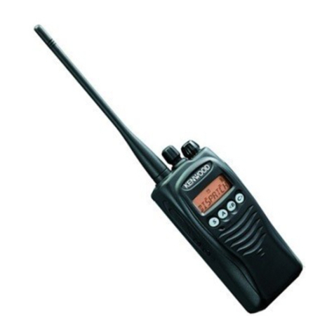
Icom IC-E92D User manual

S-14416XZ-C1
Jan. 2008
VHF/UHF DIGITAL TRANSCEIVER

This service manual describes the latest service information
for the IC-E92D VHF/UHF DIGITAL TRANSCEIVER at the
time of publication.
NEVER connect the transceiver to an AC outlet or to a DC
power supply that uses more than specifed. This will ruin
the transceiver.
DO NOT reverse the polarities of the power supply when
connecting the transceiver.
DO NOT apply an RF signal of more than 20 dBm (100 mW) to
the antenna connector. This could damage the transceiver’s
front-end.
To upgrade quality, any electrical or mechanical parts and
internal circuits are subject to change without notice or
obligation.
MODEL VERSION SUPPLIED
CHARGER
IC-E92D [EUR] BC-167D
Be sure to include the following four points when ordering
replacement parts:
1. 10-digit Icom parts numbers
2. Component name
3. Equipment model name and unit name
4. Quantity required
<ORDER EXAMPLE>
1110003491 S.IC TA31136FNG IC-E92D MAIN UNIT 5 pieces
8820001210 SCREW 2438 SCREW IC-E92D Top cover 3 pieces
Addresses are provided on the inside back cover for your
convenience.
Icom, Icom Inc. and logo are registered trademarks of Icom Incorporated (Japan) in the United States, the United
Kingdom, Germany, France, Spain, Russia and/or other countries.
ORDERING PARTS
1. Make sure the problem is internal before disassembling
the transceiver.
2. DO NOT open the transceiver until the transceiver is
disconnected from its power source.
3. DO NOT force any of the variable components. Turn
them S-Lowly and smoothly.
4. DO NOT short any circuits or electronic parts. An
insulated tuning tool MUST be used for all adjustments.
5. DO NOT keep power ON for a long time when the
transceiver is defective.
6. DO NOT transmit power into a Standard Signal
Generator or a Sweep Generator.
7. ALWAYS connect a 50 dB to 60 dB attenuator between
the transceiver and a Deviation Meter or Spectrum
Analyzer when using such test equipment.
8. READ the instructions of test equipment throughly
before connecting a test equipment to the transceiver.
REPAIR NOTES
INTRODUCTION
CAUTION
UNIT ABBREVIATIONS:
F=FRONT UNIT
L=LOGIC UNIT
M=MAIN UNIT
R=RF UNIT
V=VCO UNIT

CONTENTS
SECTION 1 SPECIFICATIONS
SECTION 2 INSIDE VIEWS
SECTION 3 DISASSEMBLY INSTRUCTION
SECTION 4 CIRCUIT DESCRIPITON
4-1 RECEIVER CIRCUITS. . . . . . . . . . . . . . . . . . . . . . . . . . . . . . . . . . . . . . . . . . . . . . . . . . . . . . . . 4-1
4-2 TRANSMITTER CIRCUITS . . . . . . . . . . . . . . . . . . . . . . . . . . . . . . . . . . . . . . . . . . . . . . . . . . . . 4-5
4-3 FREQUENCY SYNTHESIZER CIRCUITS . . . . . . . . . . . . . . . . . . . . . . . . . . . . . . . . . . . . . . . . 4-6
4-4 CPU PORT ALLOCATION . . . . . . . . . . . . . . . . . . . . . . . . . . . . . . . . . . . . . . . . . . . . . . . . . . . . . 4-7
4-5 VOLTAGE DIAGRAMS. . . . . . . . . . . . . . . . . . . . . . . . . . . . . . . . . . . . . . . . . . . . . . . . . . . . . . . . 4-8
SECTION 5 ADJUSTMENT PROCEDURES
5-1 PREPARATION . . . . . . . . . . . . . . . . . . . . . . . . . . . . . . . . . . . . . . . . . . . . . . . . . . . . . . . . . . . . . 5-1
5-2 TRANSMIT AMPLIFIER ADJUSTMENT . . . . . . . . . . . . . . . . . . . . . . . . . . . . . . . . . . . . . . . . . . 5-3
5-3 FREQUENCY ADJUSTMENT . . . . . . . . . . . . . . . . . . . . . . . . . . . . . . . . . . . . . . . . . . . . . . . . . . 5-10
5-4 DEVIATION ADJUSTMENTS . . . . . . . . . . . . . . . . . . . . . . . . . . . . . . . . . . . . . . . . . . . . . . . . . . 5-11
5-3 RECEIVE ADJUSTMENTS . . . . . . . . . . . . . . . . . . . . . . . . . . . . . . . . . . . . . . . . . . . . . . . . . . . . 5-14
5-3 FREQUENCY ADJUSTMENT . . . . . . . . . . . . . . . . . . . . . . . . . . . . . . . . . . . . . . . . . . . . . . . . . . 5-10
SECTION 6 PARTS LIST
SECTION 7 MECHANICAL PARTS
SECTION 8 BOARD LAYOUTS
SECTION 9 BLOCK DIAGRAM
SECTION 10 VOLTAGE DIAGRAM

1 - 1
SECTION 1 SPECIFICATIONS
‡Selectable depending on the operating frequency band.
P GENERAL
• Frequency coverage : (unit: MHz)
Version A band B band
EUR Tx: 144–146, 430–440
Rx: 0.495–999.990*1, *2
Tx: 144–146, 430–440
Rx:
118–174*
2
, 350–470*
1
*
1Guaranteed 430–440 MHz only, *2Guaranteed 144–146 MHz only,
• Mode :
FM, FN-N, AM (Rx only), WFM (Rx only), DV
• No. of memory channels : 1304
(incl. 100 scan edges and 4 call channels)
• Usable temp. range : –20°C to +60°C
• Tuning steps : 5‡, 6.25‡, 8.33‡, 9‡, 10, 12.5, 15, 20,
25, 30, 50, 100, 125 and 200 kHz
• Frequency stability : ±2.5 ppm (–20°C to +60°C)
• Power supply : 10.0–16.0 V DC for external DC power,
or specified Icom’s battery pack
• Digital transmission speed: 4.8 kbps
• Voice coding speed : 2.4 kbps
• Current drain (at 7.4 V DC) :
Tx High 144 MHz 1.8 A typical
430/440 MHz 2.1 A typical
Tx Mid. 144 MHz 1.2 A typical
430/440 MHz 1.5 A typical
Tx Low 144 MHz 0.6 A typical
430/440 MHz 0.7 A typical
Tx S-Low 0.4 A typical
Rx Rated output 150 mA typical (single watch; FM)
180 mA typical (dualwatch; FM/FM)
200 mA typical (single watch; DV)
220 mA typical (dualwatch; FM/DV)
Rx Power save 38 mA typical
(single watch; FM)
(Duty 1:4)
43 mA typical (dualwatch; FM/FM)
47 mA typical (single watch; DV)
50 mA typical (dualwatch; FM/DV)
standby 65 mA typical (single watch; FM)
90 mA typical (dualwatch; FM/FM)
110 mA typical (single watch; DV)
130 mA typical (dualwatch; FM/DV)
• Antenna connector : SMA (50 Ω)
• Dimensions : 59(W)×112(H)×34.2(D) mm;
(projections not included)
• Weight (approx.) : 325 g (with antenna and BP-256)
P TRANSMITTER
• Modulation system :
FM Variable reactance freq. modulation
DV (Digital) GMSK reactance freq. modulation
• Output power (at 7.4 V DC)
(Typical) : High 5.0 W, Mid. 2.5 W, Low 0.5 W,
S-Low 0.1 W
• Max. frequency deviation : ±5.0 kHz (FM wide: approx.)
±2.5 kHz (FM narrow: approx.)
• Spurious emissions : Less than –60 dBc at High/Mid.
Less than –13 dBm at Low/Slow
• Ext. mic. impedance : 2 kΩ
P RECEIVER
• Receive system :
Except WFM Double-conversion superheterodyne
WFM Triple-conversion superheterodyne
• Intermediate frequencies :
1st A band 61.65 MHz/59.25 MHz (WFM only)
B band 46.35 MHz
2nd 450 kHz/13.35 MHz (WFM only)
3rd 1.95 MHz (WFM only)
• Sensitivity (except spurious points):
AM
(1 kHz/30% Mod.; 10 dB S/N)
0.495–4.995 MHz 1.3 µV typ.
5.000–29.995 MHz 0.56 µV typ.
118.000–137.000 MHz 0.5 µV typ.
222.000–246.995 MHz 0.79 µV typ.
247.000–329.995 MHz 1 µV typ.
FM
(1 kHz/3.5 kHz Dev.; 12 dB SINAD)
VHF (Amateur band only) 0.14 µV typ.
UHF (Amateur band only) 0.16 µV typ.
1.625–29.995 MHz 0.4 µV typ.
30.000–117.995 MHz 0.25 µV typ.
118.000–173.995 MHz 0.14 µV typ.
174.000–259.995 MHz 0.32 µV typ.
260.000–349.995 MHz 0.32 µV typ.
350.000–469.995 MHz 0.16 µV typ.
470.000–599.995 MHz 0.32 µV typ.
600.000–999.990 MHz 0.56 µV typ.
WFM
(1 kHz/52.5 kHz Dev.; 12 dB SINAD)
76.000–108.000 MHz 1 µV typ.
175.000–221.995 MHz 1.8 µV typ.
470.000–770.000 MHz 2.5 µV typ.
DV
(digital/PN9 4.8 kbps; BER 1%)
VHF (Amateur band only) 0.22 µV typ.
UHF (Amateur band only) 0.22 µV typ.
• Audio output power : More than 200 mW at 10% distortion
(at 7.4 V DC) with an 8 Ωload
• Selectivity :
FM (Wide), AM More than 50 dB
FM (Narrow), DV More than 45 dB
WFM More than 300 kHz/–3 dB
Less than 700 kHz/–20 dB
• Ext. speaker connector : 3-conductor 3.5(d) mm; (1⁄8˝)/8 Ω
• Spurious and image rejection ratio :
VHF More than 60 dB
UHF More than 50 dB
(Intermediate freq.; More than 60 dB)
• Squelch Sensitivity (except spurious points):
AM (1 kHz/30% Mod.)
0.495–4.995 MHz 1.3 µV typ.
5.000–29.995 MHz 0.56 µV typ.
118.000–137.000 MHz 0.5 µV typ.
222.000–246.995 MHz 0.79 µV typ.
247.000–329.995 MHz 1 µV typ.
FM (1 kHz/3.5 kHz Dev.)
1.625–29.995 MHz 0.4 µV typ.
30.000–75.995 MHz 0.25 µV typ.
76.000–117.995 MHz 0.25 µV typ.
118.000–173.995 MHz 0.14 µV typ.
174.000–259.995 MHz 0.32 µV typ.
260.000–349.995 MHz 0.32 µV typ.
350.000–469.995 MHz 0.16 µV typ.
470.000–599.995 MHz 0.32 µV typ.
600.000–999.990 MHz 0.56 µV typ.
WFM
(1 kHz/52.5 kHz Dev.)
76.000–108.000 MHz 1 µV typ.
175.000–221.995 MHz 1.8 µV typ.
470.000–770.000 MHz 2.5 µV typ.

2 - 1
SECTION 2 INSIDE VIEWS
ANALOG SWITCH
(IC50: CD4066)
• LOGIC UNIT
RS-232 DRIVER
(IC52: MAX3221)
EEPROM
(IC51: 24LC512)
CPU3V REGULATOR
(IC100: R1150H022)
AF SWITCH
(IC301: TC7W53)
MODEM
(IC501: CMX589)
AF FILTER/IDC
(IC302: LMV324)
AF BUFFER
(IC504: NJM2115)
LINER CODEC
(IC503: AD73311)
DC-DC CONVERTER
(IC101: XC6371A551PR)
CPU CLOCK
(X1: CR-864)
AF PWR AMP
(IC400: NJM2070)
DATA I/O INVERTER
(IC33: TC7W04FU)
SHIFT REGISTER
(IC53: CD4094)
AF PWR AMP REGULATOR
(Q400: 2SB1201)
DC SWITCH
(Q100: HAT1024R)
DSP CODEC
(IC506: AMBE-2020)
CPU
(IC1: HD64F2239)
SWITCHING REGULATOR
(IC102: XC9201C05)

2 - 2
TONE FILTER
(IC150: LM2904)
IF IC (A BAND)
(IC100: TA31136FNG)
IF IC (A BAND)
(IC200: TA31136FNG)
(TOP VIEW)
• RF UNIT
(B-BAND)
DISCRIMINATOR
(X100: JTBM450)
RX VCOs (B BAND)
(TOP VIEW)
• MAIN UNIT
(BOTTOM VIEW)
(BOTTOM VIEW)
2ND IF FILTER (A BAND)
(FI100: LTWC450E1)
(B BAND)
DISCRIMINATOR
(X200: JTBM450)
D/A CONVERTER
(IC950: M62352)
D/A CONVERTER
(IC951: M62352)
APC CONTROLLER
(IC150: NJM3404)
TONE SELECTOR
(IC703: CD4066)
(B BAND)
2ND IF FILTER
(FI200: LTWC450E1)
(B BAND)
1st IF FILTER
(FI50: FL-335)
D/A CONVERTER
(IC600: M62364FP)
SHIFT REGISTER
(IC702: CD4094)
SHIFT REGISTER
(IC701: CD4094)
(B BAND)
2ND IF FILTER
(FI201: LTWC450E1)
AF FILTER
(IC502: NJM2904)
AF FILTER
(IC501: NJM2904)
VCO UNIT
(Under the cover)
TX POWER AMP
(Q100: 2SK3476)
HEAT SINK for
TX POWER AMP
(MP100: 2888 PA HEATSINK)
TX DRIVE AMP
(Q101: 2SK3475) DC SWITCH
(Q1000: HAT1026)

3 - 1
SECTION 3 DISASSEMBLY INSTRUCTION
1. Removing the front panel
qUnscrew 6 screws from the CHASSIS.
w
Disconnect the flat cable between MAIN UNIT and
FRONT assembly, and remove the FRONT assembly from
the CHASSIS.
3. Removing outer parts
qRemove the dial knobs.
wRemove the rubber cap, and unscrew the ANT nut.
eUnscrew the side screws, and remove the side panel.
2. Removing the FRONT UNIT
qUnscrew 8 screws from the FRONT UNIT.
wUnsolder 2 points to remove the speaker leads, then
remove the FRONT UNIT from the front panel.
Flat cable
FRONT assy
CHASSIS Unsolder
2 points
Speaker leads
FRONT UNIT
Front panel
ANT nut
Rubber cap
Dial knobs
Side panel
Side screws
(Contiued to next page)

3 - 2
4. Removing MAIN UNIT
qUnscrew 3 screws from the MAIN UNIT.
wUnsolder 6 points at the control dial, and remove the
MAIN UNIT.
MAIN UNIT
Unsolder
6 points
Control dial
Unsolder
4 points
RF UNIT
Unsolder
1 point
5. Removing RF UNIT
qUnsolder 4 points at the contact pins.
wUnsolder 1 point at the bottom of ANT connector.
eUnscrew 7 screws from the RF UNIT, and remove the RF
UNIT from the CHASSIS.
RF UNIT
Chassis

4 - 1
SECTION 4 CIRCUIT DESCRIPTION
• 118–173.995 MHz
The RX signals are passed through two LPFs, ANT SW,
ATT and band SW, then applied to the RF AMP (Q400). The
amplified RX signals are passed through the tuned BPF,
and applied to another RF AMP (Q401). The amplified RX
signals are passed through tuned BPF, then applied to the
1st IF mixer (IC900) via the band SW.
• 174–259.995 MHz
The RX signals are passed through the LPF, HPF, ANT SW,
ATT, band SW, HPF and another band SW insequence,
then applied to the RF AMP (Q300) via the tuned BPF. The
amplified RX signals are passed through another tuned BPF,
then applied to another RF AMP (Q301). The amplified RX
signals are applied to the 1st mixer (IC900) via the band SW.
• 260–349.995 MHz and 470–599.995 MHz
The RX signals are passed through the LPF, HPFANT SW,
ATT, BAND SW and tuned BPF in sequence, then applied to
the RF AMP (Q500). The amplified RX signals are passed
through another 2pole tuned BPF, and applied to another
RF AMP (Q501). The amplified RX signals are then applied
to the 1st mixer (IC900) via the band SW.
• 350–469.995 MHz
The RX signals are passed through the LPF, HPF, ANT
SW, ATT, band SW and HPF in sequence, then applied to
the RF AMP (Q600). The amplified RX signals are passed
through the tuned BPF, and applied to the RF AMP (Q601).
The amplified RX signals are passed through the BPF, then
applied to the 1st mixer (IC900) via the band SW.
4-1 RECEIVER CIRCUITS
RF CIRCUITS (RF UNIT)
RX signals from the antenna are sorted by its frequency by
the filters and gone through RF circuits for each bands. And
this transceiver also has two RX lines for two independent
operating bands; A BAND and B BAND.
<A BAND>
• 76 MHz and below
The RX signals are passed through two LPFs, ANT SW,
ATT, band SW and LPF. The RX signals are sorted by its
frequency by band SWs.
• 0.495–29.995 MHz
The RX signals are passed through the band SW (D201)
and LPF, and applied to tuned RF AMP (Q200). The
amplified RX signals are applied to the 1st mixer (IC900) via
the band SW (D203).
• 30–75.995 MHz
The RX signals are passed through the band SW (D250)
and tuned BPF, and applied to the RF AMP (Q250). The
amplified RX signals are passed through tuned BPF, then
applied to the 1st IF mixer (IC900) via the band SW (D256).
• 76–117.995 MHz
The RX signals are passed through two LPFs, ANT SW, ATT,
band SW, LPF and another band SW in sequence, then applied
to the RF AMP (Q300) via the tuned BPF. The amplified RX
signals are passed through another tuned BPF, then applied to
another RF AMP (Q301). The amplified RX signals are applied
to the 1st mixer (IC900) via the band SW (D311).
• RF CIRCUITS
RF
AMP
ANT
SW
RF
AMP
RF
AMP
LPF
BAND
SW
BPF
ATT
BAND
SW
RF
SW
RF
AMP
BAND
SW
RF
SW
LPF
BAND
SW
BPF
BPF
RF
AMP
HPF
RF
SW
BPF
HPF
BPF
BAND
SW ATT
RF
AMP
LPF
BAND
SW
RF
AMP
BPF
RF
AMP
BPF
LPF
BPF
RF
AMP
RF
SW
BAND
SW
ATT
LPF
BPF
BAND
SW
RF
AMP
BPF
BPF
BAND
SW
BPF
RF
AM P
ANT
SW
RF
AMP
BAND
SW
BAND
SW
BAND
SW
BAND
SW
BPF
BAND
SW
BAND
SW
BPF
BAND
SW
BPF
RF
AMP
RF
AMP
HPF
BPF
D9
Q1,2,150
D1,3,4,10,151,160
Q1,3,D6-8
D304,305
Q601
D604,605
D606
D400
D702
Q401
Q701
D402,403
D405
D200
D250
D254,255
D508
D253
D705
D603
D311
D655
Q400
Q700
Q450
D454
D201
Q500
D252
D600
D300
D650,651
Q300
Q651
D653,654
D302
D700
D401
D703,704
D404
D706
D451,452
D500
Q200
D503
D251
D256
Q600
D301
D306-309
D652
Q301
D303
D 701
D450
D453
D5
D501,502
D203
D504,507
Q250
Q501
D202
D601,602
To 1st mixer
(IC50)
for B BAND
To 1st mixer
(IC900)
for A BAND
D310
A:0.5−30MHz
A:30−76MHz
Tx:430.000−450.000MHz
Tx:144.000−148.000MHz
A:174−260MHz
A:76−118MHz
A:118−174MHz
B:118−174MHz
A:470−600MHz
A:260−350MHz
A:350−470MHz
A:350−470MHz
B:350−470MHz
A:600−1000MHz
HPF
L1-3
C1-6
L4,C7-9
L200,201
C201-204
L300,301
C301-305
L600,608
C600-602,630,631
L8,9
C18-20
L302,303
C306-310
L202,203
C205-9
L5-7
C10-14

4 - 2
• 600–999.990 MHz
The RX signals are passed through the HPF, band SW, ATT
and tuned BPF in sequence, then applied to the RF AMP
(Q700). The amplified RX signals are passed through the
BPF, and applied to another RF AMP (Q701). The amplified
RX signals are applied to the 1st mixer (IC900) via the band
SW.
The RF attenuation which reduces RX signal level to –10 dB is
carried out by D5, D9 and D701, by turning these PIN diodes
ON using "ATT" signal.
1ST IF CIRCUIT (MAIN UNIT)
<A BAND>
The RX signals from the RF circuits are applied to the 1st
mixer (RF: IC900) to be converted into the 1st IF signal,
by being mixed with the 1st Local Oscillator (LO) signals
from the VCO UNIT. The 1st LO signals from the VCO UNIT
are applied to the 1st mixer via the LO SW, or doubler (in
receiving of 600 MHz and above).
The converted 1st IF signal is passed through the IF SW (D2)
which toggles the path of the 1st IF signaL: WFM mode or
other than WFM mode.
• FM/AM MODE
The 1st IF signal from the 1st mixer (RF: IC900) is entered
to the MAIN UNIT, and passed through the 1st IF filter (FI1)
via IF SWs (D2, 3) to remove unwanted signals. The filtered
1st IF signals are applied to the 1st IF AMP (Q100), and the
amplified 1st signal is applied to the 2nd IF circuit.
<B BAND>
• 118–173.995 MHz
The RX signals for B BAND are passed through 2 LPFs,
ANT SW, ATT and band SW, then applied to the RF AMP
(Q400). The amplified RX signals are passed through
the BPF, and applied to the tuned RF AMP (Q450). The
amplified RX signals are passed through tuned 2-pole BPF,
then applied to the 1st mixer (M: IC50) via the band SW.
• 350–469.995 MHz
The RX signals are passed through the LPF, HPF, ANT SW,
ATT, band SW and another HPF in sequence, then applied
to the RF AMP (Q600). The amplified RX signals are
passed through 2-pole tuned BPF, and applied to tuned RF
AMP (Q651). The amplified RX signals are passed through
another tuned BPF, then applied to the 1st mixer (M: IC50)
via the band SW.
• WFM MODE (Incl. 2nd IF circuit)
When receiving in WFM mode, the 1st IF signal from the 1st
mixer (RF: IC900) is entered to the MAIN UNIT and passed
through the BPF, then applied to the 1st IF AMP (Q1). The
amplified 1st IF signal is applied to the 2nd mixer (Q2) to
converted into the 13.35 MHz 2nd IF signal, by being mixed
with the 45.9 MHz 2nd LO signal (generated by X450,
tripled by Q451). The converted 2nd IF signal is passed
through the 2nd IF filter (FI2) to remove sideband noise,
then applied to the 2nd IF AMP (Q100) via the IF SW (D3).
The amplified 2nd IF signal is applied to the 3rd IF circuit.
Q1
R18
Q2
C6
D2
R14
C29
C8
C17
C24
C10
D10
R11
C12
R25
D3
R15
L10
C19
FI1
1
IN
2OUT 3
GND
4GND
56
C3
R8
C20
0
.01
C
102
C30
C16
C792
R9
5
L1
0.01
C9
C5
R17
6.8K
R101
R10
R6
FI2
IO
C13
C7
L30
R23
8
0
0R7
C18
C4
1st IF filter
2nd mixer
2nd IF filter
1st IF AMP
FM/AM mode
WFM mode
1st IF filter
<B BAND>
The RX signals from the RF circuits are entered to the MAIN
UNIT, and applied to the 1st mixer (IC50) to be converted
into the 1st IF signal, by being mixed with the 1st Local
Oscillator (LO) signals from the B BAND VCO (Q350, 351)
via the buffer (Q353). The converted 1st IF signal is passed
though the 1st IF filter (FI50) to remove unwanted signals,
then applied to the 1st IF AMP (Q200). The amplified 1st IF
signal is applied to the 2nd IF circuits.
C51
C50
C54
X200
R202
C52
R201
R
209
C205
C206
C58
Q200
C207
C60
FI50
1
IN
2OU T 3
GND
4GND
56
C208
C204
R52
R51
L200
R205
EP50
C203 C57
IC50
1
RFI
2
GND
3
LO
4PS
5VCC
6IFO
C59
L50
1st IF filter
1st mixer
1st IF AMP
BAND RX MODE 1st IF 1st LO 2nd IF 2nd LO 3rd IF 3rd LO
A BAND NFM/AM 61.65 MHz 62.15–538.345 MHz (<600 MHz)
269.175–469.17 MHz (>600 MHz) 450 kHz 61.2 MHz - -
WFM 59.25 MHz 16.75–355.375 MHz(76–770 MHz) 13.35 MHz 45.9 MHz 1.95 MHz 15.3 MHz
B BAND NFM/AM 46.35 MHz 71.65–423.65 MHz
(118–174, 350–470 MHz) 450 kHz 45.9 MHz - -
• FREQUENCY CONFIGULATION
• 1ST IF CIRCUIT (For FM/AM mode) AND 2ND IF CIRCUIT (For WFM mode) (A BAND)
• 1st IF CIRCUIT (B BAND)

4 - 3
2ND IF AND DEMODULATOR CIRCUITS
(MAIN UNIT)
<A BAND>
The 1st IF signal from the 1st IF AMP (Q100) is applied to
the IF IC (IC100). The applied 1st IF signal is mixed with
the 61.2 MHz 2nd LO signal (generated by X450, buffered
by Q450) at the internal 2nd mixer, to be converted into the
2nd IF signal. The converted 2nd IF signal is output from pin
3, then passed through the 2nd IF filter (FI100) via IF SWs
(D102, 103).
• FM MODE
The filtered 2nd IF signal is backed to the IF IC from
pin 5, and saturation-amplified by the internal limit AMP.
The amplified 2nd IF signal is FM-demodulated by the
discriminator (X100), and the recovered AF signals (RX
AF signals) are output from pin 9, then applied to the AF
circuits via the AF mute SW (IC500, pins 8, 9).
• AM MODE
The filtered 2nd IF signal is amplified by 2nd IF AMP (Q103),
then applied to the AM demodulator circuit (Q104, 105,
D105) to be recovered to the AF signals. The demodulated
AF signals are applied to the AF circuits.
<B BAND>
The 1st IF signal from the 1st IF AMP (Q200) is applied to
the IF IC (IC200). The applied 1st IF signal is mixed with
45.9 MHz 2nd LO signal (generated by X450, tripled by
Q451) at the internal 2nd mixer, to be converted into the
450 kHz 2nd IF signal. The converted 2nd IF signal is output
from pin 3, then passed through one of the 2nd IF filters.
The 2nd IF signal is passed through FI200 in FM/AM mode,
and passed through FI1201 in FM-N mode.
• FM/FM-N/DV MODE
The filtered 2nd IF signal is backed to the IF IC from pin
5, then saturation-amplified by the internal limit AMP.
The amplified 2nd IF signal is FM-demodulated by the
discriminator (X200), and the recovered AF signals (RX
AF signals) are output from pin 9, then applied to the AF
circuits via the AF mute SW (IC500, pins 4, 3).
• AM MODE
The filtered 2nd IF signal is amplified by another 2nd
IF AMP (Q202), then applied to the AM demodulator
circuit (Q203, 204, D205) to be AM-demodulated. The
demodulated AF signals are applied to the AF circuits.
C113
X100
C124
R107
R114
R117 R108
C111
C126
C123
IC100
1OSCIN
2OSCOUT
3MIXOUT
4VCC
5IFIN
6DEC
7FILOUT
8FILIN 9
AFOUT
10
QUAD
11
IFOUT
12
RSSI
13
N-DET
14
N-REC
15
GND
16
MIXIN
C138
C116
C114
FI100
IO
R116
R119
D102
C136
R111
C125
C117
0
C
D103 R106
L101
C122
R115
C108
C137
R112
C115
4
5
R113 C121
R118 C109
C112
R105
C143
C134
47K
R124
R131
R120
C133
R123
C130
.1
1
31
R121
R122
Q104
1
2
34
5
6
C142
R133
R127
R125
C129
R130
C135
D104
R126
R132
D105
100
C128
C127
Q103
1
2
34
5
6
1
1
44
AM demodulator
2nd IF AMP
for AM mode
3RD IF CIRCUIT (MAIN UNIT)
(FOR A BAND, WFM MODE ONLY)
The 2nd IF signal from the 2nd IF AMP (Q100) is applied to
the IF IC.
The applied 2nd IF signal is mixed with the 15.3 MHz 3rd
LO signal (generated by X450, buffered by Q450), to be
converted into the 1.95 MHz 3rd IF signal by the internal 3rd
mixer. The converted 3rd IF signal is output from pin 3, and
passed through the IF SWs (D102, 103), then backed to the
IF IC (bypassing FI100). The 3rd IF signal is FM-demodulated
by the discriminator (X100), and the recovered AF signals
(RX AF signals) are output from pin 9, then applied to the AF
circuits via the AF mute SW (IC500, pins 8, 9).
C237
R227
IC200
1OSCIN
2OSCOUT
3M IXOUT
4VCC
5IFIN
6DEC
7FILOUT
8FILIN 9
AFOUT
10
QUAD
11
IFOUT
12
RSSI
13
N-DET
14
N -REC
15
GND
16
MIXIN
EP200
C236
C213
C212
R231
R210
X200
C220
C211
R214
R209
C206
C215
C221 C207
0.1
C241
C216
FI200
IO
C208
C222
C214
D202
R205
C238
FI201
IO
C224
R215
C223
R216
R206
C225
D203
R218
R220
R221
C230
K
5
Q202
1
2
34
5
6
C232
R233
R217
C233
R224
Q203
1
2
34
5
6
D205
R234
1
6
2
R306
100
C229
D204
1
C261
0
.1
2
34
R219
R223
C226
C227
C228
C231
R225
R305
AM demodulator
2nd IF AMP
for AM mode
• 2ND IF AND FM DEMODULATOR CIRCUITS (A BAND)
• 2ND IF AND FM DEMODULATOR CIRCUIT (B BAND)
• AM DEMODULATOR CIRCUIT (A BAND)
• AM DEMODULATOR CIRCUIT (B BAND)

4 -4
RX AF CIRCUITS (LOGIC UNIT)
<A BAND>
The AF signals from the FM/AM demodulator circuits are
passed through the mode SW (M: IC500D) and one of the
AF filters (IC502 and Q501, or, Q502 only) whose audio
frequency response is set as stable for each RX mode (FM/
AM or WFM).
FM/AM-demodulated AF signals are filtered by IC502, and
FM (WFM)-demodulated AF signals are filtered by Q502.
The filtered AF signals are passed through the D/A
converter (DAC; IC600, pins 21, 22; 24, 23) for level
adjustment. The level-adjusted AF signals are entered to the
LOGIC UNIT via the RX AF mute SW (M: IC700, pins 8, 9),
and applied to the AF power AMP (IC400) to obtain audio
output power. The power-amplified AF signals are applied to
the internal speaker or output from [DATA/SP/MIC] jack.
<B BAND>
• FM MODE
The FM-demodulated AF signals from the mute SW (M:
IC500B) are passed through the mode SW (IC500A) and
AF filter (M: IC501).
• AM MODE
The AM-demodulated AF signals from the AM detector (M:
Q203, 204, D205) are directly passed through the AF filter
(M: IC501, pin 2).
• DV MODE
The FM-demodulated signals from the IF IC (M: IC200) are
passed through the tone filter (M: IC250). The filtered signals
are applied to the modem (IC501) via the tone selector (M:
IC703) and buffer (IC504B), to be converted into the DV data.
The DV data is applied to the CPU (IC1), and converted into
the AMBE signals. The AMBE signal is then applied to the
DSP CODEC IC (IC506) and decoded. The decoded AMBE
signals are converted into the analog audio signal by liner
CODEC IC (IC503). The converted AF signals are passed
through the mode SW (M: IC500A) and AF filter (M: IC501).
The filtered AF signals are passed through the D/A
converter (DAC; M: IC600, pins 13, 14; 16, 15) for level
adjustment. The level-adjusted AF signals are entered to
the LOGIC UNIT via RX AF mute SW (M: IC700C/D), and
applied to the AF power AMP (IC400) to obtain audio output
power. The power-amplified AF signals are applied to the
internal speaker or output from [DATA/SP/MIC] jack.
SP
AF
AMP
BUFF
LPF
LPF
CPU
Q400,401
POWER AMP
CONTROLLER
MODEM
DSP
CODEC
LINEAR
CODEC
IC600
IC400
LOGIC UNIT MAIN UNIT
CHASSIS
[DATA/MIC/SP]
IC503
IC506
IC504B
IC501
IC1
SP
SW
FIL
IC501
SEL
SW
IC150
SW
FILTER
FILTER
FIL
IC500A
M ODE
TONE
IC500D
M ODE
IC250
AF
IC703
<B-BAND>
FM-demodulated
AF signals from IF IC (IC200)
<B-BAND>
FM-demodulated
AF signals from MUTE SW (IC500)
FM-demodulated AF signals from IF IC (IC200)
Level-adjusted AF signals to IF IC (IC200)
Level-adjusted AF signals to IF IC (IC100)
FM-demodulated AF signals from IF IC (IC100)
<B-BAND>
AM-demodulated
AF signals from AM demodulator (D205)
<A-BAND>
AM/FM-demodulated AF signals from
AM demodulator (D105)/mute SW (IC500)
TONE
TONE
AF
D/A
AFON
SPSW
Q402-405
IC502
AF
FIL
Q502
RX AF MUTE
SW
11
13
1
2
3
8
7
11
9
2
2
2
7
14
6711
20,21
72,73
3297
42
16
15
8
2
11
37
10
69,10
IC700C/D:CD4066
22 21
11
12
9
10
24
23
SQUELCH CIRCUIT
The squelch circuit cuts off the AF output signals when
no RF signals are received. Detecting noise components
(approx. 30 kHz signals) in the demodulated AF signals, the
squelch circuit stops audio signals being emitted.
A portion of FM-demodulated AF signal from the IF IC
(M: IC100/IC200) is passed through the DAC (M: IC600)
for level (=threshould) adjustment. The level-adjusted AF
signals are passed through the noise filter (IC100, pins 7, 8
and R111–113, C121, 122/IC200, pins 7, 8 and R214–216,
C221, 222) to filter the noise components (approx. 30 kHz
signals) only. The noise components are rectified to produce
DC voltage corresponding to the noise level.
If the noise level is higher than the preset one, the internal
comparator set the "ANOISE"/"BNOISE" signal to the
CPU to "High", then the CPU turns the "AFON" signal
which controlls the AF power AMP (L: IC400) to "Low," to
inactivate the AF power AMP (L: IC400). At the same time,
the CPU turns the "ARMUTE"/"BRMUTE" signal which
controlls the RX AF mute SW (L: IC700) to "Low," to cut-off
the RX AF line.
DAC Noise
AMP
Noise filter
From IF IC
(IC100, Pin16)
To RX AF circuits
Noise
detector
Com-
parator
NOISE SQUELCH DIAGRAM (A BAND)
“ANOIS”
IC600
IC100
9
8
7
13
10
DAC Noise
AMP
Noise filter
From IF IC
(IC200, Pin16)
To RX AF circuits
Noise
detector
Com-
parator
NOISE SQUELCH DIAGRAM (B BAND)
“BNOIS”
IC600
IC200
9
8
7
13
10
• RX AF CIRCUITS

4 - 5
• TX AF CIRCUITS
4-2 TRANSMIT CIRCUITS
TX AF CIRCUITS (LOGIC UNIT)
• FM MODE
MIC signals from the internal/external microphone (MIC
signals) are passed through the MIC gain SW (Q303),
and applied to the MIC AMP (Q302, 304). The amplified
MIC signals are passed through the mode SW (IC301)
which toggles the MIC line according to the operating
mode; FM or DV. The MIC signals are applied to the IDC
(Instance Deviation Controller; IC302) circuit which limits
the amplitude of MIC signals (=deviation) to prevent over
deviation.
The amplitude-limited MIC signals are passed through the
splatter filter (IC302) which cuts off the 3 kHz and higher
audio signals. The frequency-limited MIC signals are entered
to the MAIN UNIT via the mode SW (IC303), then applied
to the DAC (M: IC600) for level (deviation) adjustment. The
level-adjusted MIC signals are applied to the modulation
circuits.
Modulation signals
to the VCO UNIT
MC300
MIC
AM P
BUFF
BUFF
LPF
ID C LPF
ALC
AM P
CPU
MODEM
DSP
CODEC
LINEAR
CODEC
SW
MODE
IC302B
IC302C
IC302D
IC600
Q306,307
Q309
LOGIC UNIT
IC503
IC504A
IC506
IC501,502
IC1
MAIN UNIT
D/A
Q302,304
MODE
SW
IC301
IC300
CTCSS
SW
GAIN
IC303
Q303
From ext. microphone
1
6
7
1
2
16
5798
5
21
?
?
12 14
7
• DV MODE
The MIC signals from the microphone (MC300) are passed
through the MIC gain SW (Q303) and applied to the MIC
AMP (Q302, 304). The amplified MIC signals are applied
to the ALC AMP (IC300) which automatically adjusts the
level of MIC signals to stable for digital proccessing, via
the mode SW (IC301). The level-adjusted MIC signals are
applied to the IDC circuit (IC302) for amplitude-limitting.
The amplitude-limited MIC signalsn are passed through the
splatter filter (IC302) which cuts off the 3 kHz and higher
audio signals.
The frequency-limited MIC signals are applied to the liner
CODEC IC (IC503) via the buffer (IC504A), and encoded
into the digital audio signal. The digital audio signal is then
applied to the DSP CODEC IC (IC506) and converted into
the AMBE signal. The AMBE signal is applied to the modem
IC (IC501) via the CPU (IC1). The modem IC converts
the AMBE signal into the analog signal, and output to the
DAC (IC600, pin 1) via the buffer (IC302D) and the mode
SW (IC303). The tone signal is level-adjusted by DAC
(M: IC600), then applied to the modulation circuits as the
modulation signals.
MODULATION CIRCUITS (VCO UNIT)
The modulation signals from the DAC (M: IC600, pin 2)
are entered to the VCO UNIT, and applied to the variable
capacitors of VCOs.
• OPERATING ON VHF BAND
The modulation signals are applied to the D55 of the
VHF VCO (Q51, D51, 54) to obtain FM modulation. The
FM-modulated VCO output is buffer-amplified by Q200,
amplified by Q201 then entered to the RF UNIT as TX
signal.
• OPERATING ON UHF BAND
The modulation signals are applied to the D100 of the UHF
VCO (Q101, D101, 104) to obtain FM modulation. The
FM-modulated VCO output is buffer-amplified by Q200,
amplified by Q201 then entered to the RF UNIT as TX
signal.
TX AMPLIFIERS (RF UNIT)
TX signal from VCO UNIT is applied to the LO AMP
(IC100) via the LO SW (D100). The amplified TX signal is
passed through the ATT (D158, 159) which is a port of the
APC circuit. The level-adjusted TX signal is amplified by
YGR (Q102), drive (Q101) and power (Q100) amplifiers in
sequence, to obtain TX output power. The power-amplified
TX signal is passed through the TX filters, power detector
and ANT SWs.
• OPERATION ON VHF BAND
The power-amplified TX signal from the power AMP (Q100)
is passed though the LPF, power detector, ANT SW and two
LPFs (as a harmonic filter), then applied to the antenna via
ANT connector (CHASSIS; J1).
• OPERATION ON UHF BAND
The power-amplified TX signal from the power AMP (Q100)
is passed though the BPF, power detector, ANT SW, HPF
and LPF (as a harmonic filter), then applied to the antenna
via ANT connector (CHASSIS; J1).

4 - 6
• FREQUENCY SYNTHESIZER CIRCUITS (A BAND)
4-3 FREQUENCY SYNTHESIZER CIRCUITS
VCOs
This transceiver has total of five VCOs; one RX VCO and
RX/TX VCOs on the VCO UNIT, and two RX VCOs on the
MAIN UNIT.
<A BAND>
• BC BAND VCO (VCO UNIT; Q1, D1, 3, 5, 6)
The BC BAND VCO generates the 1st LO for BC band (0.495
–75.995 MHz) RX.
• VHF BAND VCO (VCO UNIT; Q51, D51, 54)
The VHF BAND VCO generates the 1st LO for VHF band (76
–173.995 MHz) RX, and also TX signal for the operation on
the VHF band.
• UHF BAND VCO (VCO UNIT; Q101, D101, 104)
The UHF BAND VCO generates the LO for UHF band (174
–599.995 MHz) RX, and also TX signal for the operation on
the UHF band.
When receiving 600 MHz and higher signals, the UHF BAND
VCO oscillates 269.175–469.17 MHz 1st LO signals, and the
output signal is doubled by the doubler (MAIN UNIT; Q850,
D851) before being applied to the mixer (MAIN UNIT; IC900).
<B BAND>
• VHF BAND VCO (MAIN UNIT; Q301, D300, 301)
The VHF BAND VCO generates the 1st LO for VHF band
(118–174 MHz) RX for B BAND.
• UHF BAND VCO (MAIN UNIT; Q351, D350, 352)
The UHF BAND VCO generates the 1st LO for UHF band
(350–470 MHz) RX for B BAND.
PLLs
The PLL circuit provides stable oscillation for both of the
transmit and 1st LO frequencies. By comparing the fedback
VCO output and the reference frequency signal, the oscillating
frequency is stabilized. The PLL output frequency is controlled
by the serial data including divide ratio from the CPU.
<A BAND> (VCO AND MAIN UNITS)
A portion of output signals from each VCO are fedback
to the PLL IC (M: IC800) via buffers (V: Q200, 202) and
LPF. The applied VCO outputs are divided by the prescaler
and programmable divider, then phase-compared with
divided reference frequency from X450 (MAIN). The phase
difference is output via the charge pump, and applied to the
VCOs as lock voltage via the loop filter.
<B BAND> (MAIN UNIT)
A portion of output signals from each VCO are fedback
to the PLL IC (IC400) via buffer (Q353). The applied VCO
outputs are divided by the prescaler and programmable
divider, then phase-compared with divided reference
frequency from X450. The phase difference is output via the
charge pump, and applied to the VCOs as lock voltage via
the loop filter.
When the oscillation frequency drifts, its phase changes
from that of the reference frequency, causing a lock voltage
change to compensate for the drift in the VCO oscillating
frequency.
APC CIRCUIT (RF UNIT)
The APC (Automatic Power Control) circuit stabilizes
transmit output power to prevent transmit output power level
change which is caused by load mismatching or heat effect,
etc.
TX signal is passed through the power detector (VHF; D154
–156/UHF; D150, 152,153). The power detector rectifies
a portion of the TX signal and converts it into DC voltage
which is in proportion to the transmit output power. The
detected voltage is applied to the APC controller (IC150B).
The TX power setting voltage “PSET” is applied to another
input terminal as the reference voltage.
The output voltage is applied to the ATT (D158, 159) to con-
trol the attenuation level, to adjust the input level of the YGR
AMP (Q102) so that the TX output power is stable.
The setting of TX power is carried out by applying voltage
“DSET” to the APC controller (IC150A).
The output voltage of
the controller controls the bias of the drive and power AMPs
to reduce/increase the gain of these amplifiers to set the TX
output power to High, Mid., Low and S-Low.
ATT ANT
SW
PWR
DET
PWR
AM P LPF
LPF
APC
CTRL
YGR
AM P DRIVE
AM P
LPF
GATE
CTRL
HPF
TX/RX
SW
PWR
DET
ANT
SW
LO
AMP BPF
D158,159
IC150B
PSET
D6,7
Q100Q102
D1
Q101
IC100
D 100,850
IC150A
Q152 L1-3
C1-6
L100.101.153
C100-103,192
L102,103
C106,107
L5-7
C10-14
L4,C7-9
ANT
Q153
D154-156
D150,152,153
DSET
VHF TX signal
UHF TX signal
X3
X4
BUFF
VCO
FIL
LOOP VCO
PLL
IC
BUFF
Q300,301,D300,301
15.3 MHz
X450,D451
Q450
VHF: 164.350-220.350MHz
MODE
Q353,D351
Q451,D452
UHF: 333.650-426.345MHz
SW
IC50
Q350,351,D350,D352
IC400
Q452
Q151,453,D450
FILTER
LOOP
VCO
BUFF
BUFF
PLL
IC
VCO
LO
AMP
VCO
LPF
RF UNIT
Q201
IC800
UHF:
319.175-538.345MHz
VCO UNIT
Q101,102,100-102,104
Q1,2,D1-3,5,6
Q51,52,D1,2,4,5
Q200
BC: 62.145−131.645MHz
Q202
VHF:
131.350-235.645MHz
15.3MHz reference frequency
Modulation signals
• TX AMPLIFIERS AND APC CIRCUIT
• FREQUENCY SYNTHESIZER CIRCUITS (B BAND)

4 - 7
LINE
NAME DESCRIPTION IN/OUT STATUS CONDITION
POWER [POWER] key input. (Pull-up). IN L –
PKEY [PWR] key input (Pull-up). IN L The key is pushed
DICK [DIAL] input(Phase A). IN – –
DIUD [DIAL] input(Phase B). IN – –
PTT [PTT] key input (Pull-down). IN H The key is pushed
SQL [SQL] key input (Pull-up). IN L The key is pushed
I0–I3 Initial matrix ports. IN – –
KR0–KR4 Key detect signal.
(Pushed bottom is detected according to the input voltage.) IN – –
KS0–KS3 Key matrix ports. OUT – –
ESIO Serial data to the EEPROM. IN/OUT – –
ECK Clock to the EEPROM. OUT – –
TXC T6 line regulator (M: Q650–652) control signal. OUT H While transmitting.
BLED [BUSY] LED driver (L: Q201) control signal. OUT H RX(Squelch open)
LIGHT LCD/Key backlight driver (L: Q202) control signal. OUT L Lights ON.
LCDDT Serial data to the LCD driver (L: DS1). OUT – –
LCDCS Chip select signal to the LCD driver (L: DS1). OUT – –
LCDCK Clock to the LCD driver (L: DS1). OUT – –
LCDRS Strobe signal to the LCD driver (L: DS1). OUT – –
LCDRES Reset signal to the LCD driver (L: DS1). OUT – –
AMBEC DSP IC power line regulator (L:IC508) control signal. OUT H In DV mode operation.
DVC Liner CODEC IC power line regulator (L: Q503,504) control signal. OUT H In DV mode operation.
TX232 RS-232 data (TXD). OUT – –
RX232 RS-232 data (RXD). IN – –
TXCK TX clock to the modem (L: IC501). IN – –
TXDT TX data to the modem (L: IC501). OUT – –
RXCK RX clock to the modem (L: IC501). IN – –
RXDT RX data to the modem (L: IC501). IN – –
ACQ ACQ signal to the modem (L: IC501). OUT H Synchronized
DCEL DCEL signal to the modem (L: IC501). OUT H Synchronized
AMBERES Reset signal to the liner CODEC IC and DSP CODEC IC (L: IC503 and
IC506). OUT – –
AMBECLK AMBE clock signal to the DSP CODEC IC (L: IC506). OUT – –
AMBESTB AMBE strobe signal to the DSP CODEC IC (L: IC506). OUT – –
AMBETXD AMBE TX data to the DSP CODEC IC (L: IC506). OUT – –
AMBERXD AMBE RX data to the DSP CODEC IC (L: IC506). IN – –
AMBEEPR AMBE EPR signal to the DSP CODEC IC (L: IC506). IN – –
CLSFT Clock frequency shift signal to the clock oscillator (L:X1, D13). OUT H
DICK2 [DIAL] (VR) input (Phase A). IN – –
DIUD2 [DIAL] (VR) input (Phase B). IN – –
CHGC Charging control signal to the charge circuit (L:Q150–153, D150, 151) OUT H While charging.
CHGH Charging current control signal to the charging controller (L: Q150, 152). OUT H Charging current increase.
CPUHV Externalpower supply detection. IN L External power supply is
connected.
AFON Control signal to the AF power AMP controller (L: Q400, 401). OUT H AF power AMP (L: IC400) is
activated (Squelch open).
BATT Power supply select signal to the power supply selector (L: IC50, Q53). OUT H/L
H=Operated by the battery pack.
L=Operated by an external
power source.
SPSW Speaker select signal to the Internal speaker SW (L: Q402–405). OUT – –
ANOIS Noise detect signal from the A BAND IF IC (M: IC100). IN – –
BNOIS Noise detect signal from the B-AND IF IC (M: IC200). IN – –
CK Common clock signal to the the PLL ICs and DAC (LMX2313/
ME15E03SL/M62352AGP). OUT – –
DATA Common serial data to the PLL ICs and DAC (LMX2313/ME15E03SL/
M62352AGP). OUT – –
4-4 CPU PORT ALLOCATION

4 - 8
4-5 VOLTAGE BLOCK DIAGRAMS
Voltage from the attached battery pack is routed to the whole of the transceiver via regulators and switches.
LINE
NAME DESCRIPTION IN/OUT STATUS CONDITION
DASTB1 Strobe signal to the DAC (R: IC950). OUT – –
DASTB2 Strobe signal to the DAC (M: IC600). OUT – –
IOSTB1 Strobe signal to the expander (R: IC951). OUT – –
IOSTB3 Strobe signal to the expanders (M: IC701, 702). OUT – –
IOSTB4 Strobe signal to the expander (L: IC53). OUT – –
APLLSTB Strobe signal to the A BAND PLL IC (M: IC800). OUT – –
BPLSTB Strobe to the B BAND PLL IC (M: IC400). OUT – –
BPS Power save mode control signal to the A/B BAND PLL ICs (M: IC800/
IC400). OUT L In power save mode.
UNLK Unlock signal from the A BAND PLL IC (M: IC800). IN H PLL is locked.
CLIN Key detect signal. (Pushed bottom is detected by refering input voltage.) IN A/D –
ATONE Tone signals; tone and WX A BAND. IN A/D –
BTONE Tone signals; tone and WX B BAND. IN A/D –
VIN DC voltage divided by the voltage detect resisters (L: R159 and R160).
(Remaining battery capacity detection.) IN A/D –
OPTV External device detect. IN A/D –
TEMP The voltage in proportion to the internal temperature.
The voltage divided by R66 (thermistor; LOGIC) and R67 (LOGIC). IN A/D –
S-TXV
• While operated by battery
RSSI voltage from the IF IC (M: IC100).
• While perated by external power supply
Current in TX from the I-V converter (M: IC704).
IN A/D –
BRSSI RSSI voltage from the B BAND IF IC (M: IC200). IN A/D –
CTCOUT CTCSS/DTCS signals. OUT D/A –
DTMF Tone signals; DTMF, EUR tone, OUT D/A –
RESET Reset signal from the reset IC (L:IC100). IN H –
DC-IN VCC +5V +3CPU CPU
DC
SW
SW
REG
V5.5+
V3+
V3+
V3+
R3V
T
Q1000,
D1000, 1001 IC102
Q650−652
Q400,401
IC100
Q800,801,830
IC103 IC101,D101
Q202
Q150−153
D150, 151
TAB
Battery pack
T5
NOCP
CHGH CHGC TXC
VCOA, B, C
AF PWR AMP
(IC400)
LIGHT
COCVC
COCVB
COCVA
AFON
C3R
V3䇭EBMAV5D
AMBEC
MEDOM
CVD
CODEC CODEC
3V
CHG
MAINR3V
RFR3V
T6
AF6V
REG
DC-DC
LED3V
MODEM3V
REG
+3V
REG
VCO3V
AMBE
REG
4-4 CPU PORT ALLOCATION (continued)

5 - 1
SECTION 5 ADJUSTMENT PROCEDURE
5-1 PREPARATION
¤ REQUIRED INSTRUMENTS
INSTRUMENTS SPECIFICATION INSTRUMENTS SPECIFICATION
DC Cable OPC-254L (Optional product) JIG cable
(See the illust below)
Power Supply Output voltages : 5.0–13.5 V DC
Current capacity : More than 3 A Multimeter Input impedance : 50 kΩ
Measuring range : 0.1–10V/0.01–5 A
RF Power Meter
(terminated type)
Measuring range : 0.1–10 W
Frequency range : 100–500 MHz
Impedance : 50
Ω
SWR : Less than 1.2 : 1
Standard Signal
Generator (SSG)
Frequency range : 0.1–1000 MHz
Output level : 0.04 µV to 32 mV
(–28 dBu to 90 dBu)
Frequency Counter
Frequency range : 0.1–600 MHz
Frequency accuracy : ±1 ppm or better
Input level : Less than 1 mW
AC Millivoltmeter Measuring range : 10 mV to 10 V
Attenuator Power attenuation : 30 dB
Capacity : More than 10 W
Modulation
Analyzer
Frequency range : 30–600 MHz
Measuring range : 0 to ±10 kHz Audio Generator Frequency range : 300–3000 Hz
Output level : 1–500 mV
¤ JIG CABLE CONNECTION
CAUTION!: BACK UP originally programmed contents (Memory channels, Common settings, etc.) in the transceiver using optional
RS-92 REMOTE CONTROL SOFTWARE before starting adjustment.
When all adjustments are completed, these contents in the transceiver will be cleared.
OPC-1797
(Optional product)
3-conductor 2.5 (d) mm
[MIC]
To the [DATA/MIC/SP] jack
JIG cables
[SP]
plug
(MIC)
(GND)
33 k
+−
AC
MILLIVOLTMETER
(10 mV to 10 V)
AUDIO GENERATOR
(300–3000 Hz/1–500 mV)
+−
PTT
+
4.7 µF
3-conductor 3.5 (d) mm plug
(CLONE)
(GND)
1 kΩ
(4
#(/
5.1

5 - 2
MENTERING ADJUSTMENT MODE
qTurn the power OFF.
wConnect
the JIG cable to the [DATA/SP/MIC] jack.
eWhile pushing [SQL] and [8] keys, turn the power ON.
MKEY ASSIGNMENTS FOR THE ADJUSTMENT MODE
MQUITTING ADJUSTMENT MODE
qTurn the power OFF.
wWhile pushing [VFO], [MR] and [BAND] keys, turn the power ON. (All reset)
Adjusts the value for the item
Stores adjustment value
Starts automatic adjustment
Selects previous adjustment item
Selects next adjustment item
(without storing value)
(4
#(/
5.1
[SQL] Adjustment frequency
Adjustment value
Adjustment item
[PWR]
[8]
(4
(4
#(/
#(/
5.1
5.1
TX power
Band: Mode
During adjustment mode, the display shows adjustment conditions as above.

5 - 3
5-2 TRANSMIT AMPLIFIER ADJUSTMENT
Select an adjustment item using [2] / [8] keys, then set the adjustment value as specified using [DIAL].
ADJUSTMENT ADJUSTMENT CONDITION OPERATION
ADJUSTMENT
ITEM VALUE
IDLING CURRENT
(@5.0 V)
[PREPARATION]
0 • Supply voltage : 5.0 V 1) Connect an RF power meter
to the antenna connector.
2) Connect a multimeter
between the external power
supply and transceiver.
––
[VHF BAND] 1 • Displayed freq. : ""
• Transmitting
• Adjust the current using
[DIAL], then release the PTT
and push [BAND] to store the
adjustment value.
[KF]200–300
mA
[UHF BAND] 2 • Displayed freq. : ""
• Transmitting
TRANSMIT
POWER (@5.0 V)
[VHF (BAND LOW)]
1 • Displayed freq. : ""
• TX power : "5.1"
• Transmitting
• Adjust the TX power using
[DIAL], then release the PTT
and push [BAND] to store the
adjustment value.
[2Q] 50–150 mW
[VHF (BAND HIGH)] 2 • Displayed freq. : ""
• TX power : "5.1"
• Transmitting
[UHF (BAND LOW)] 3 • Displayed freq. : ""
• TX power : "5.1"
• Transmitting
[UHF (BAND HIGH)] 4 • Displayed freq. : ""
• TX power : "5.1"
• Transmitting
To the battery contact pins
JIG cable
(See the page 5-1)
5.0 V
Fusese
(3A)
DC power supply
⊕
−
–
+
MULTIMETER
(10 mA to 3 A)
+
−
RF POWER METER
(10 W/50 Ω)
Be sure the polarity.
(4
#(/
5.1

5 - 4
5-2 TRANSMIT AMPLIFIER ADJUSTMENT (continued)
Select an adjustment item using [2] / [8] keys, then set the adjustment value as specified using [DIAL].
ADJUSTMENT ADJUSTMENT CONDITION OPERATION
ADJUSTMENT
ITEM
VALUE
IDLING
CURRENT (@7.4 V)
[PREPARATION]
0 • Supply voltage : 7.4 V 1) Connect an RF power meter
to the antenna connector.
2) Connect a multimeter
between the external power
supply and transceiver.
––
[VHF BAND]
(Hi power)
1 • Displayed freq. : ""
• TX power : "*K"
• Transmitting
• Adjust the current using
[DIAL], then release the PTT
and push [BAND] to store the
adjustment value.
[KF]
1.1– 1.2 A
(Mid power) 2 • Displayed freq. : ""
• TX power : "/KF"
• Transmitting
600–700
mA
(Low power) 3 • Displayed freq. : ""
• TX power : ".QY"
• Transmitting 200–300
mA
(S-Low power) 4 • Displayed freq. : ""
• TX power : "5.1"
• Transmitting
[UHF BAND]
(Hi power)
5 • Displayed freq. : ""
• TX power : "*K"
• Transmitting
1.1– 1.2 A
(Mid power) 6 • Displayed freq. : ""
• TX power : "/KF"
• Transmitting
600–700
mA
(Low power) 7 • Displayed freq. : ""
• TX power : ".QY"
• Transmitting 200–300
mA
(S-Low power) 8 • Displayed freq. : ""
• TX power : "5.1"
• Transmitting
To the battery contact pins
JIG cable
(See the page 5-1)
7.4 V
RF POWER METER
(10 W/50 Ω)
Fusese
(3A)
DC power supply
⊕
−
Black
White
MULTIMETER
(10 mA to 3 A)
+
−
Be sure the polarity.
(4
#(/
5.1
Other manuals for IC-E92D
2
This manual suits for next models
1
Table of contents
Other Icom Transceiver manuals