4 - 4
4-2 TRANSMITTER CIRCUITS
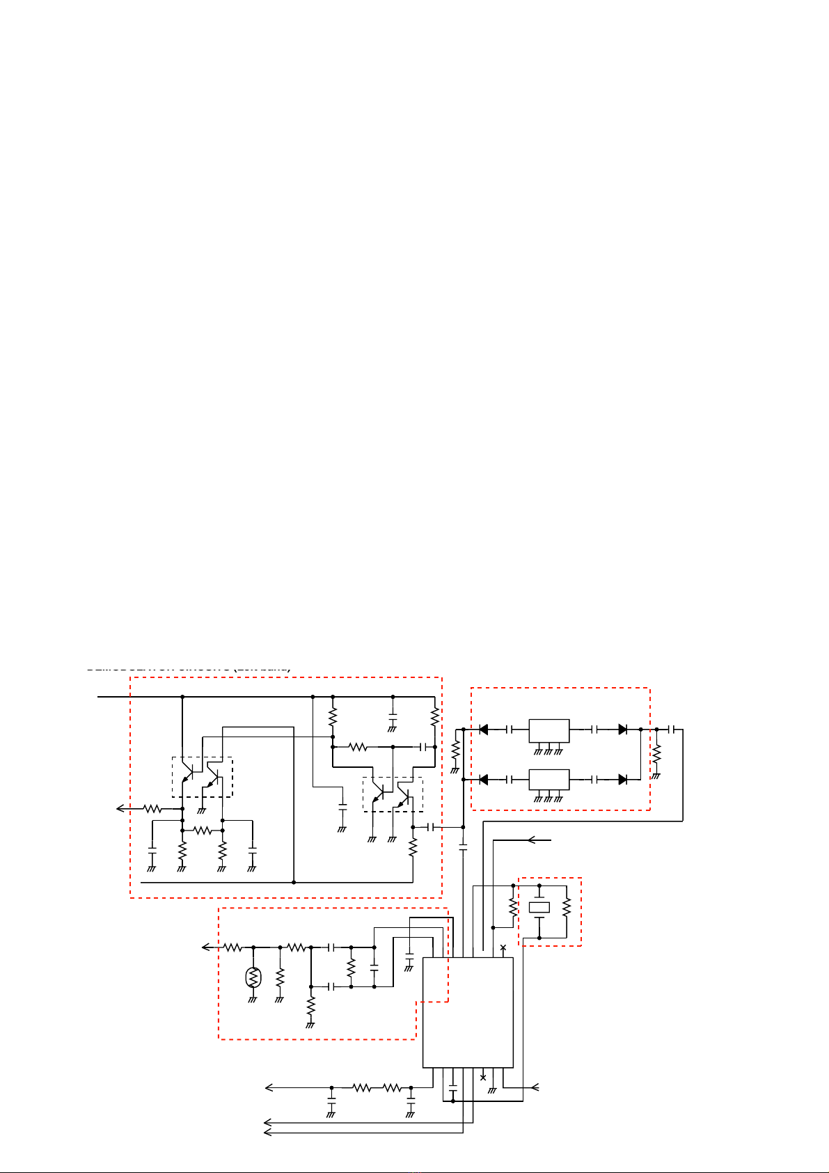
MICROPHONE AMPLIFIER CIRCUITS
The audio signals from the microphone (MIC signals) are
applied to the microphone amplifier (IC28) via J2 and HPF
(Q87). The amplified MIC signals are passed through the
microphone gain switch (Q88) and MIC mute switch (IC30),
then passed through or by-passed ALC amplifier (IC32) via
AF switches (IC29 and IC52).
The MIC signals from the AF switch (IC52) are passed
though the HPF (IC48), LPF (IC48) and AF switch (IC51),
and then applied to the AF amplifier (IC48). The amplified
MIC signals are applied to the D/A converter (IC8) for level
(deviation) adjustment. The level adjusted MIC signals are
applied to the VCO as the modulation signals via modulation
signal selector.
<OPERATION ON THE LEFT BAND>
The modulation signals are applied to the variable capacitor
D147 of the left band VCO (Q111, D145–147) via the
modulation selector (IC9) and modulation mute switch
(Q109), and modulated. The modulated VCO output are
amplified by the buffer (Q113) and LO amplifier (IC44), and
applied to the transmit amplifiers as the TX signal, via the LO
switches (D155, 157), LPF(L157, C818, 820) and attenuator
(R33, 37, 46).
TRANSMIT POWER AMPLIFIERS
TX signal from the attenuator (R33, 37, 46) is amplified by
pre-drive (Q25) and drive (Q27) amplifiers to obtain RF level
for power module (IC3). The amplified TX signal is applied
to the power amplifier which is a VHF band PA module
composed by two power MOS-FETs. The power-amplified
TX signal is passed through the LPF, power detector,
antenna switch (D59) and LPF, before being applied to the
antenna connector (CHASSIS; J1).
APC CIRCUITS
A portion of the TX signal from IC3 is rectified at the power
detector (D39, D47), and converted into the DC voltage
which is in proportion to the RF power, and applied to the
operational amplifier (IC4, pin 6). IC4 is an APC amplifier
for both of V/UHF bands. The TX power setting voltage
“PCON_V” from the D/A converter (IC1, pin 7) is applied
to the pin 5 as a reference. IC4 is rolled as a differential
amplifier which outputs voltage in inverse proportion to
rectified one. When the TX power increased, the rectified
voltage also increased, that causes the decrease of output
voltage of differential amplifier. The decrease of output
voltage of differential amplifier causes the drop of the gate
voltage of IC3, Thus the TX power maintained to keep stable
level.
TX muting is carried out by TX mute SW (Q36) controlled
by “TX_mute” signal. Applying “TX_mute” signal to the base
terminal of Q36 to turn it ON, 8 V DC appears on the pin 6 of
IC4 and its output voltage downs to 0 V DC to inactivate IC3.
SQUELCH CIRCUITS
• NOISE SQUELCH
A portion of FM-demodulated AF signals from the IF IC
(IC18, pin 9) are level-adjusted by D/A converter (IC8), and
passed throuhgh the noise fltier (IC18 and some R and C) to
be filtered noise components (30 kHz and above signals) in
the AF signals. The filtered noise components are detected
in the IC18 and output from pin 13, then applied to the CPU
as “R_SQL” signal.
Then the CPU outputs “R_AF_MUTE” signal from pin 51 to the
speaker mute switch (Q102), according to the “R_SQL” signal
level. Thus the AF line is connected to the GND to turn the AF
output OFF.
• CTCSS/DTCS
CTCSS/DTCS signals in the demodulated AF signals from
the AF switch (IC16) are passed through the tone filter (Q42)
. The filtered CTCSS/DTCS signals are applied to the CPU
IC12) as “R_DTCS” signal.
The CPU (IC25) compares the applied signal and the set
CTCSS/DTCS, then outputs control signal as same as “NOISE
SQUELCH.”
R764
R784
C656
R589
C625
R765
IC30
1
2
C620
C636
R767
C687
R802
C644
R804
C623 C624
IC48
1
2
3
5
6
7 8
9
10
12
13
14
C855
C856
R763
C645
R578
IC51
1
6
7
R664
R575
C619
5VS
R660
R628
R527
R545
C649
C648
R785
R532
33K
R533
R547
IC28
1
2
3
4
5
C866
R537
R560
R562
R577
R774
C862
AN6123MS
IC32
1
VCC
2
DET
3INPUT
4GND
5OUTPUT
R801
R574
C857
R766
R541
C637
R771
R775
R762
IC29
1
6
7
C635
Q88
Q87
R549
C858
C861
R550
R640
IC52
1
6
7
R538
R566
MIC_SENC
MIC signals from
the microphone
• MICROPHONE AMPLIFIER CIRCUITS
Modulation signals
to the modulation circuits
HPF Microphone
amplifier
ALC
MIC
mute
switch
HPF
HPF
LPF
Amplifier
AF switch
AF
switch
AF
switch
• DTMF
DTMF signals in the demodulated AF signals from the AF
switch (IC16) are passed through two AF switches (IC57
and IC58), then applied to the DTMF decoder (IC56) to be
decoded.
AF CIRCUITS
The AM/FM-demodulated AF signals from the AF switch
(IC12) are passed through the AF filter (Q48). The filtered
AF signals are applied to the electric volume (IC33) to be
adjusted its level. The level-adjusted AF signals are applied
to the dual AF power amplifiier (IC38) to obtain AF output
power level, then applied to the an external speaker via
external speaker jack (J8).