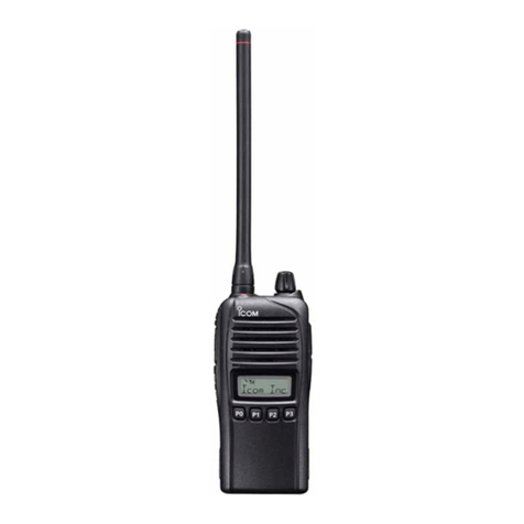
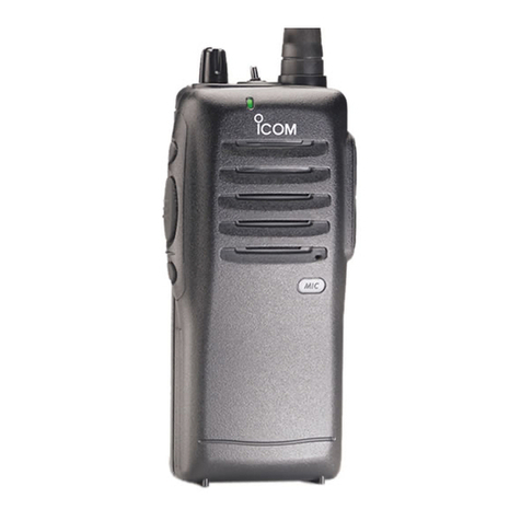
Icom IC-F3 User manual

Count on us!
6-9-16, Kamihigashi, Hirano-ku, Osaka 547-0002, Japan A-5452MI-S-1
© 1997 Icom Inc.
SERVICE
MANUAL
VHF FM TRANSCEIVERS
iC-f3
iC-f3s
UHF FM TRANSCEIVERS
iC-f4
iC-f4s
iC-f3 iC-f3s iC-f4 iC-f4s
*IC-F3/F3S,F4/F4S cover(GB) 99.6.8 3:24 PM Page 1

REPAIR NOTES
1. Make sure a problem is internal before disassembling the transceiver.
2. DO NOT open the transceiver until the transceiver is disconnected from its power source.
3. DO NOT force any of the variable components. Turn them slowly and smoothly.
4. DO NOT short any circuits or electronic parts. An insulated tuning tool MUST be used for all adjustments.
5. DO NOT keep power ON for a long time when the transceiver is defective.
6. DO NOT transmit power into a signal generator or a sweep generator.
7. ALWAYS connect a 40 dB or 50 dB attenuator between the transceiver and a deviation meter or spectrum analyser when
using such test equipment.
8. READ the instructions of test equipment thoroughly before connecting equipment to the transceiver.
INTRODUCTION
DANGER
This service manual describe the latest information for the
IC-F3/IC-F3S and IC-F4/IC-F4S at the time of publication.
NEVER connect the transceiver to an AC outlet or to a DC
power supply that uses more than 16 V. Such a connection
could cause a fire hazard and/or electric shock.
DO NOT expose the transceiver to rain, snow or any
liquids.
DO NOT reverse the polarities of the power supply when
connecting the transceiver.
DO NOT apply an RF signal of more than 20 dBm (100
mW) to the antenna connector. This could damage the
transceiver’s front end.
Be sure to include the following four points when ordering
replacement parts:
1. 10-digit order numbers
2. Component part number and name
3. Equipment model name and unit name
4. Quantity required
<SAMPLE ORDER>
1110001810 S.IC TA7368F IC-F3S MAIN UNIT 1 piece
8810009510 Screw B0 2 ×4 NI-ZU IC-F4 MAIN PCB 6 pieces
Addresses are provided on the inside back cover for your
convenience.
ORDERING PARTS
IC-F3 IC-F4S
6-9-16, Kamihigashi, Hirano-ku, Osaka 547-0002, Japan
Phone : 06 6793 5302
Fax : 06 6793 0013
Communication Equipment
Himmelgeister Str. 100, D-40225 Düsseldorf, Germany
Phone: 0211 346047 Fax : 0211 333639
URL : http://www.icomeurope.com
Unit 9, Sea St., Herne Bay, Kent, CT6 8LD, U.K.
Phone: 01227 741741 Fax : 01227 741742
URL : http://www.icomuk.co.uk
Zac de la Plaine, Rue Brindejonc des Moulinais
BP 5804, 31505 Toulouse Cedex, France
Phone: 561 36 03 03 Fax : 561 36 03 00
URL : http://www.icom-france.com
Crta. de Gracia a Manresa Km. 14,750
08190 Sant Cugat del Valles Barcelona, SPAIN
Phone: (93)589 46 82 Fax : (93)589 04 46
<
Corporate Headquarters
>
2380 116th Avenue N.E., Bellevue, WA 98004, U.S.A.
Phone: (425)454-8155 Fax : (425)454-1509
URL : http://www.icomamerica.com
<
Customer Service
>
Phone: (425)454-7619
A.C.N. 006 092 575
290-294 Albert Street, Brunswick, Victoria, 3056, Australia
Phone: 03 9387 0666 Fax : 03 9387 0022
URL : http://www.icom.net.au
6F No. 68, Sec. 1 Cheng-Teh Road, Taipei, Taiwan R.O.C.
Phone: (02) 2559 1899 Fax : (02) 2559 1874
A Division of Icom America Inc.
3071 #5 Road, Unit 9, Richmond, B.C., V6X 2T4, Canada
Phone: (604)273-7400 Fax : (604)273-1900
*IC-F3/F3S,F4/F4S cover(GB) 99.6.8 4:16 PM Page 2

TABLE OF CONTENTS
SECTION 1 SPECIFICATIONS
SECTION 2 INSIDE VIEWS
2 - 1 IC-F3/S................................................................................................................................................2-1
2 - 2 IC-F4/S................................................................................................................................................2-2
SECTION 3 DISASSEMBLY AND OPTION INSTRUCTIONS
3 - 1 DISASSEMBLY INSTRUCTION..........................................................................................................3-1
3 - 2 OPTIONAL UNIT INSTALLATIONS ....................................................................................................3-2
SECTION 4 CIRCUIT DESCRIPTION
4 - 1 RECEIVER CIRCUITS........................................................................................................................4-1
4 - 2 TRANSMITTER CIRCUITS.................................................................................................................4-2
4 - 3 PLL CIRCUIT ......................................................................................................................................4-3
4 - 4 POWER SUPPLY CIRCUITS..............................................................................................................4-3
4 - 5 CPU PORT ALLOCATIONS................................................................................................................4-4
SECTION 5 ADJUSTMENT PROCEDURES
5 - 1 PREPARATION...................................................................................................................................5-1
5 - 2 PLL ADJUSTMENT for IC-F3/S ..........................................................................................................5-3
5 - 3 TRIMMER ADJUSTMENT for IC-F3/S................................................................................................5-4
5 - 4 TRANSMITTER ADJUSTMENT for IC-F3/S.......................................................................................5-5
5 - 5 RECEIVER ADJUSTMENT for IC-F3/S..............................................................................................5-6
5 - 6 PLL ADJUSTMENT for IC-F4/S..........................................................................................................5-7
5 - 7 TRIMMER ADJUSTMENT for IC-F4/S................................................................................................5-8
5 - 8 TRANSMITTER ADJUSTMENT for IC-F4/S.......................................................................................5-9
5 - 9 RECEIVER ADJUSTMENT for IC-F4/S............................................................................................5-10
SECTION 6 PARTS LIST
6 - 1 IC-F3/S................................................................................................................................................6-1
6 - 2 IC-F4/S................................................................................................................................................6-5
SECTION 7 MECHANICAL PARTS AND DISASSEMBLY
SECTION 8 SEMI-CONDUCTOR INFORMATION
SECTION 9 BOARD LAYOUTS
9 - 1 IC-F3/S MAIN UNIT.............................................................................................................................9-1
9 - 2 VR BOARD..........................................................................................................................................9-1
9 - 3 IC-F4/S MAIN UNIT.............................................................................................................................9-3
SECTION 10 BLOCK DIAGRAM
10 - 1 IC-F3/S..............................................................................................................................................10-1
10 - 2 IC-F4/S..............................................................................................................................................10-2
SECTION 11 VOLTAGE DIAGRAM
11 - 1 IC-F3/S ..............................................................................................................................................11-1
11 - 2 IC-F4/S ..............................................................................................................................................11-2

All stated specifications are subject to change without notice or obligation.
Frequency coverage
Type of emission
Number of channels
Power supply requirement
TX at High
Current drain at Low
(approx.) RX rated audio
stand-by
Frequency stability
Usable temperature range
Dimensions (proj. not included)
Weight (BP-196)
Output power
Modulation system
Max. freqequency deviation
Spurious emissions
Adjacent channel power
Transmitter audio distortion
Limitting charact of modulator
Ext. microphone connector
Receive system
Intermediate frequencies
Sensitivity (typical)
Squelch sencitivity
(at threshold)
Adjcent chnnel selectivity
Spurious response
Intermoduration rejection ratio
Audio output power
(at 9.6 V DC)
External SP connector
IC-F3/F3S IC-F4/F4S
RECEIVER TRANSMITTER GENERAL
400.000–430.000 MHz (L-band)
136.000–150.000 MHz (L-band) 440.000–470.000 MHz (ML-band)
470.000–500.000 MHz (MH-band)
146.000–174.000 MHz (H-band) 490.000–512.000 MHz (H1-band)
490.000–520.000 MHz (H2-band)
16K0F3E (W-type), 14K0F3E (M-type: F3/S only), 8K50F3E (N-type)
32 ch (16 channels ×2 banks: 2-BANK version), 16 ch (16 channel version)
9.6 V DC (negative ground; supplied battery pack)
1.3 A 1.4 A
600 mA 700 mA
250 mA 250 mA
60 mA (typ.) 60 mA (typ.)
±0.0005% (EIA), ±2000 Hz (ETS/CEPT; W, M-types), ±2.5 kHz (ETS/CEPT; N-type)
+22˚F to +140˚F (EIA) +22˚F to +140˚F (EIA)
–20˚C to +55˚C (ETS/CEPT) –30˚C to +60˚C (ETS/CEPT)
57(W) ×140(H) ×37(D) mm; 21⁄4(W) ×51⁄2(H) ×115⁄32(D) inch
390 g; 13.8 oz
High 5 W High 4 W
Low 1 W Low 1 W
Variable reactance frequency modulation
±5.0 kHz (W-type), ±4.0 kHz (M-type), ±2.5 kHz (N-type)
70 dB typical (EIA)
0.25 µW (ETS/CEPT)
70 dB typical (W, M-types)
60 dB (N-type)
Less than 5 % at 1 kHz, 60 % deviation
70–100 % of max.deviation
3-conductor 2.5(d) mm (1⁄10")/2 kΩ
Double-conversion superheterodyne system
1st: 31.05 MHz 1st: 46.350 MHz
2nd: 450 kHz 2nd: 450 kHz
0.25 µV at 12 dB SINAD 0.3 µV at 12 dB SINAD
0.63 µV (emf) at 20 dB SINAD 0.79 µV (emf) at 20 dB SINAD
0.25 µV 0.3 µV
70 dB (W, M-types)
60 dB (N-type)
70 dB
65 dB
500 mW typical at 10% distortion with a 8 Ωload
3-conductor 3.5 (d) mm (1⁄8")/8 Ω
SECTION 1 SPECIFICATIONS
1 - 1

2 - 1
F3/S
SECTION 2 INSIDE VIEWS
2-1 IC-F3/S
• MAIN UNIT
Low-pass filter circuit
Current detector circuit
RF amplifier
(Q12: 3SK239)
Crystal filter
(FI1)
T/R switching circuit
(D4: MA77)
1st mixer circuit
(Q13: 3SK166-2)
PLL reference oscillator
(X1: CR-575, 15.3 MHz)
CPU (IC8)
EEPROM (IC7)
VCO circuit
APC control circuit
Mute switch
(IC4: BU4066BCFV)
PLL IC
(IC1: µPD3140GS)
Microphone amplifier
circuit
FM IF IC
(IC2: TA31136FN)
Antenna switching
circuit (D1: MA77)
Power amplifier
(Q1: 2SK2595)
T/R switching
circuit (D3: MA77)
Expander IC
(IC10: M62354GP)
TOP VIEW BOTTOM VIEW
*IC-F3/S,F4/S.doc 99.6.14 5:17 PM Page 2 - 1

F4/S
2 - 2
2-2 IC-F4/S
• MAIN UNIT
Low-pass filter circuit
Current detector circuit
RF amplifier
(Q12: 3SK239)
Crystal filter
(FI1)
T/R switching circuit
(D4: MA77)
PLL reference oscillator
(X1: 15.3 MHz)
CPU (IC8)
EEPROM (IC7)
VCO circuit
APC control circuit
Mute switch
(IC4: BU4066BCFV)
PLL IC
(IC1: µPD3140GS)
Microphone amplifier
circuit
FM IF IC
(IC2: TA31136FN)
Antenna switching
circuit (D1: MA77)
Power amplifier
(Q1: 2SK2595)
T/R switching
circuit (D3: MA77)
Expander IC
(IC10: M62354GP)
1st mixer circuit
(Q13: 3SK241 R)
TOP VIEW BOTTOM VIEW
*IC-F3/S,F4/S.doc 99.6.14 5:17 PM Page 2 - 2

3 - 1
SECTION 3 DISASSEMBLY INSTRUCTIONS
3-1 DISASSEMBLY INSTRUCTION
• Removing the chassis panel
qUnscrew 1 nut A, and remove 1 knob B.
wUnscrew 2 screws, C.
eTake off the chassis in the direction of the arrow.
rUnplug J6 to separate front panel and chassis.
• Removing the MAIN unit
qRemove the sealing rubber.
wUnsolder 3 points Dand unscrew 1 nut E.
eUnscrew 2 screws, F, and 6 screws G(silver, 2 mm), to separate the chassis and MAIN unit.
rTake off the MAIN unit in the direction of the arrow.
Chassis C(nickel, 2 mm) × 2
J6 (Speaker connector)
Front panel
ANut
BKnob
F(black, 2 mm) ×2
Guide holes
Shield cover
(IC-F4/F4S only)
G
G
MAIN unit
Sealing rubber
ENut Chassis
G
GG
D
G(silver, 2 mm) ×6

3 - 2
3-2 OPTIONAL UNIT INSTALLATIONS
1Remove the option cover.
2Remove the bottom protective paper of sponge.
3Connect either a UT-80, UT-96 or UT-105 optional unit to J5.
4Attached the 1556 sponge to the specified position at the unit as following illustration.
5Replace the option cover to the chassis-hole.
Option cover
Option unit
J5
SPONGE
Parts name : 1556 sponge
Order No. : 8930013545
UT-80 UT-96

SECTION 4 CIRCUIT DESCRIPTION
4 - 1
4-1 RECEIVER CIRCUITS
4-1-1 ANTENNA SWITCHING CIRCUIT
Received signals are passed through the low-pass filter
(L1–L3, C1–C7 for IC-F3/S, L1–L3, C3, C5, C7 for IC-F4/S).
The filtered signals are applied to the λ⁄4type antenna
switching circuit (D8 for IC-F3/S D406, D8 for IC-F4/S).
The antenna switching circuit functions as a low-pass filter
while receiving. However, its impedance becomes very high
while D8 (IC-F3/S)/D406 and D8 (IC-F4/S) is/are turned ON.
Thus transmit signals are blocked from entering the receiv-
er circuits. The antenna switching circuit employs a λ⁄4type
diode switching system. The passed signals are then
applied to the RF amplifier circuit.
4-1-2 RF CIRCUIT
The RF circuit amplifies signals within the range of frequen-
cy coverage and filters out-of-band signals.
The signals from the antenna switching circuit are amplified
at the RF amplifier (Q12) after passing through the tuneable
bandpass filter (D9, D10, C83 for IC-F3/S, D10, L413, C79
for IC-F4/S). The amplified signals are applied to the 1st
mixer circuit (Q13) after out-of-band signals are suppressed
at the tuneable bandpass filter (D11, D12, D21, D22, C94 for
IC-F3/S, D11, D12, D401, C94 for IC-F4/S).
Varactor diodes are employed at the bandpass filters that
track the filters and are controlled by the CPU (IC8) via the
expander IC (IC10) using T1–T4 signals. These diodes tune
the centre frequency of an RF passband for wide bandwidth
receiving and good image response rejection.
4-1-3 1ST MIXER AND 1ST IF CIRCUITS
The 1st mixer circuit converts the received signal to a fixed
frequency of the 1st IF signal with a PLL output frequency.
By changing the PLL frequency, only the desired frequency
will be passed through a crystal filter at the next stage of the
1st mixer.
The signals from the RF circuit are mixed at the 1st mixer
(Q13) with a 1st LO signal coming from the VCO circuit to
produce a 31.05 MHz (IC-F3/S) or 46.35 MHz (IC-F4/S) 1st
IF signal.
The 1st IF signal is applied to a pair of crystal filters (FI1) to
suppress out-of-band signals. The filtered 1st IF signal is
applied to the IF amplifier (Q14 for IC-F3/S, Q400 for IC-
F4/S), then applied to the 2nd mixer circuit (IC2, pin 16).
4-1-4 2ND IF AND DEMODULATOR CIRCUITS
The 2nd mixer circuit converts the 1st IF signal to a 2nd IF
signal. A double conversion superheterodyne system (which
converts receive signals twice) improves the image rejection
ratio and obtains stable receiver gain.
The 1st IF signal from the IF amplifier is applied to the 2nd
mixer section of the FM IF IC (IC2, pin 16), and is mixed with
the 2nd LO signal to be converted to a 450 kHz 2nd IF sig-
nal.
The FM IF IC contains the 2nd mixer, limiter amplifier, quad-
rature detector and active filter circuits. A 2nd LO signal
(30.6 MHz for IC-F3/S, 45.9 MHz for IC-F4/S) is produced at
the PLL circuit by dividing it’s reference frequency.
The 2nd IF signal from the 2nd mixer (IC2, pin 3) passes
through a ceramic filter (FI2) to remove unwanted hetero-
dyned frequencies. It is then amplified at the limiter amplifi-
er (IC2, pin 5) and applied to the quadrature detector (IC2,
pins 10, 11) to demodulate the 2nd IF signal into AF signals.
4-1-5 AF CIRCUIT
AF signals from the FM IF IC (IC2 pin 9) are applied to the
mute switch (IC4, pin 1) via the AF filter circuit (IC3b, pins 6,
7). The output signals from pin 11 are applied to the AF
power amplifier (IC5, pin 4) after being passed through the
[VOL] control (VR board, R1).
• 2nd IF AND DEMODULATOR CIRCUITS
Mixer
16
Limiter
amp.
2nd IF filter
450 kHz PLL IC
IC1
X1
15.3 MHz
IC2 TA31136F
12 1st IF from the IF amp.
"SD" signal to the CPU pin 98
11109
87 5 3
AF signal "DET" R5
X3
Squelch level
adjustment pot
R92
2
17 16
Active
filter
FI2
Noise
detector
FM
detector
13
"NOIS" signal to the CPU pin 19
RSSI
Noise
comp.
×2 or ×3

4 - 2
The applied AF signals are amplified at the AF power ampli-
fier circuit (IC5, pin 4) to obtain the specified audio level. The
amplified AF signals, output from pin 10, are applied to the
internal speaker (SP1) via the [SP] jack when no plug is con-
nected to the jack.
4-1-6 SQUELCH CIRCUIT
Asquelch circuit cuts out AF signals when no RF signals are
received. By detecting noise components in the AF signals,
the squelch switches the AF mute switch.
Aportion of the AF signals from the FM IF IC (IC2, pin 9) are
applied to the active filter section (IC2, pin 8) where noise
components are amplified and detected with an internal
noise detector. The squelch level adjustment pot (R92) is
connected in parallel to the active filter input (pin 8) to con-
trol the input noise level.
The active filter section amplifies noise components. The fil-
tered signals are rectified at the noise detector section and
converted into “NOIS” (pulse type) signals at the noise com-
parator section. The “NOIS” signal is applied to the CPU
(IC8, pin 19).
The CPU detects the receiving signal strength from the
number of the pulses, and outputs an “RM” signal from pin
43. This signal controls the mute switch (IC4) to cut the AF
signal line.
4-2 TRANSMITTER CIRCUITS
4-2-1 MICROPHONE AMPLIFIER CIRCUIT
The microphone amplifier circuit amplifies audio signals with
+6 dB/octave pre-emphasis characteristics from the micro-
phone to a level needed for the modulation circuit.
The AF signals from the microphone are applied to the
microphone amplifier circuit (IC3c, pin 10). The amplifiedAF
signals are passed through the low-pass filter circuit (IC3d,
pins 13, 14) via the mute switch (IC4, pins 2–4). The filtered
AF signals are applied to the modulator circuit after being
passed through the mute switch (IC4, pins 8–10) and the
deviation adjustment pot (R119; IC-F4/S only).
4-2-2 MODULATION CIRCUIT
The modulation circuit modulates the VCO oscillating signal
(RF signal) using the microphone audio signal.
The audio signals change the reactance of a diode (D6 for
IC-F3/S, D404 for IC-F4/S) to modulate an oscillated signal
at the VCO circuit (Q7, Q8). The oscillated signal is ampli-
fied at the buffer-amplifiers (Q4, Q6), then applied to the T/R
switching circuit (D3, D4).
4-2-3 DRIVE/POWER AMPLIFIER CIRCUITS
The signal from the VCO circuit passes through the T/R
switching circuit (D3) and is amplified at the buffer(s) (Q3 for
IC-F3/S, Q3, Q403 for IC-F4/S), drive (Q2) and power ampli-
fier (Q1) to obtain 5 W (IC-F3/S)/4 W (IC-F4/S) of RF power
(at 9.6 V DC). The amplified signal passes through the
antenna switching circuit (D1), and low-pass filter and is
then applied to the antenna connector.
The bias current of the drive (Q2) and the power amplifier
(Q1) is controlled by the APC circuit.
4-2-4 CURRENT DETECTOR CIRCUIT
The current detector circuit (Q9, Q28) detects the total dri-
ving current of the drive and the power amplifiers, using the
current sensor (R161). The differential amplifier (Q9) detects
the voltage difference of the current sensor input and output
voltages, then outputs control voltage to the APC circuit (IC-
F3/S only) and the CPU (IC8, pin 97).
4-2-5 POWER DETECTOR CIRCUIT (IC-F4/S ONLY)
The power detector circuit (D2) detects the transmit power
output level and converts it to DC voltage. The detected sig-
nal is applied to the APC circuit.
4-2-6 APC CIRCUIT
The APC circuit (IC3a, Q37) protects the drive and the
power amplifiers from excessive current drive, and selects
HIGH or LOW output power.
•APC circuit
Q1
Power
amp.
Q2
Driver
amp.
IC3a
+
–
T5
VCC
Q9
"ISENS" signal
to the CPU
Q28
R161
RF signal
from PLL to antenna
T4
TXC Q37
S5
Current sensor circuit
APC control circuit
IC-F3/S only
Power detector
circuit (D2; IC-F4/S only)

4 - 3
The signal output from the current sensor circuit (Q9, Q28;
IC-F3/S) or the power detector circuit (D2; IC-F4/S) is
applied to the differential amplifier (IC3a, pin 2), and the “T4”
signal from the expander (IC10, pin 14), controlled by the
CPU (IC8), is applied to the other input for reference.
When the driving current is increased, input voltage of the
differential amplifier (pin 2) will be increased. In such cases,
the differential amplifier output voltage (pin 1) is decreased
to reduce the driving current.
4-3 PLL CIRCUIT
A PLL circuit provides stable oscillation of the transmit fre-
quency and receive 1st LO frequency. The PLL output com-
pares the phase of the divided VCO frequency to the refer-
ence frequency. The PLL output frequency is controlled by
the divided ratio (N-data) of a programmable divider.
The PLL circuit contains the VCO circuit (Q7, Q8). The oscil-
lated signal is amplified at the buffer-amplifiers (Q5, Q6) and
then applied to the PLL IC (IC1, pin 2).
The PLL IC contains a prescaler, programmable counter,
programmable divider, phase detector and charge pump,
etc. The entered signal is divided at the prescaler and pro-
grammable counter section by the N-data ratio from the
CPU. The divided signal is detected on phase at the phase
detector using the reference frequency.
If the oscillated signal drifts, its phase changes from that of
the reference frequency, causing a lock voltage change to
compensate for the drift in the oscillated frequency.
A portion of the VCO signal is amplified at the buffer-ampli-
fier (Q4) and is then applied to the receive 1st mixer or trans-
mit buffer-amplifier circuit via the T/R switching diode (D3,
D4).
4-4 POWER SUPPLY CIRCUITS
VOLTAGE LINE
• PLL circuit for IC-F3/S
Shift register
×2
Prescaler
Phase
detector
Loop
filter
Programmable
counter
Programmable
divider
X1
15.3 MHz
30.6 MHz signal
to the FM IF IC
16
Q7, Q8
VCO circuit
Buffer
Q6 Buffer
Q4
Buffer
Q5
3
4
5PLST
SCK
SO
to transmitter circuit
to 1st mixer circuit
D4
D3
17
82
Line
HV
VCC
CPU5
5V
T5
R5
S5
OPT
Description
The voltage from the attached battery pack.
The same voltage as the HV line (battery volt-
age) which is controlled by the power switch
([VOL] control).
Common 5 V converted from the VCC line by
the reference regulator circuit (IC6). The output
voltage is applied to the CPU (IC8) and the 5V
regulator circuit.
Common 5 V converted from the VCC line by
the 5 V regulator circuit (Q18, Q19) using the
reference regulator (IC6).
5 V for transmitter circuits regulated by the T5
regulator circuit (Q22).
5 V for receiver circuits regulated by the R5 reg-
ulator circuit (Q21).
Common 5 V converted from the 5V line by the
S5 regulator circuit (Q20).
The same voltage as the 5V line for the optional
HM-75A or HS-51 through a resistor (R132).

4 - 4
4-5 CPU PORT ALLOCATIONS
4-5-1 CPU (IC8) CPU (IC8) — continued
Pin
number
1
11
12
13
14
15
18
19
26
36–41
(IC-F3/S)
40, 41
(IC-F4/S)
42
43
44–47
48
49
50
51
52
53
54
60–62
63
Port
name
CTCIN
CSIFT
SCK
SI
SO
UNLK
PLST
NOIS
CONT
KS0–KS5
KS4, KS5
MM
RM
KR0–KR5
R5C
S5C
TXC
T5C
LIGHT
AFON
DST
CTDA0–
CTDA2
DUSE
Description
Input port for CTCSS/DTCS signals
for decoding.
Outputs reference oscillator for the
CPU control signal.
Outputs clock signal to the PLL IC
(IC1), EEPROM (IC7) and expander
IC (IC10), etc.
Input port for the data signals from
EEPROM (IC7), etc.
Outputs data signals to the PLL IC
(IC1), EEPROM (IC7) and expander
IC (IC10), etc.
Input port for PLL unlock signal from
the PLLIC (IC1). High level signal is
applied during unlock.
Outputs strobe signals to the PLL IC
(IC1).
Input port for noise signals (pulse
type) from the FM IF IC (IC2).
Outputs LCD contrast control signal.
High: When normal level is selected
Output ports for key matrix.
Outputs mic. mute control signal.
Low: When DTMF or 2/5-tone sig-
nal is selected
Outputs RX mute control signal.
Low: When muted
Input ports for key matrix.
Outputs R5 regulator control signal.
Low: While receiving
Outputs S5 regulator control signal.
Low: While power is ON
Outputs T5 regulator control signal.
Low: While transmitting
Outputs T5 regulator control signal.
Low: While transmitting
Outputs LCD backlight control signal.
High: Lights ON
Outputs the regulator circuit for the
AF amplifier control signal.
High: While AF amp. is activated.
Outputs strobe signals to the
expander IC (IC10).
Outputs CTCSS and DTCS encode
signals (3-bit, D/A type).
Outputs filter switch control signal
for the CTCSS and DTCS (Q38).
High: DTCS is activated.
Pin
number
90
91
Port
name
MTONE
DTMF
Description
Output port for:
Beep audio while receiving.
2/5-tone signals while transmitting.
Output port for DTMF signals while
transmitting.
Pin
number
2
3
4
11–13
14
Port
name
DST
SCK
SO
T1–T3
T4
Description
Input port for strobe signals.
Input port for clock signal.
Input port for data signal.
Output tuneable bandpass filter
control voltage.
Outputs tuneable bandpass filter
control signal while receiving.
Outputs RF output power control
signals while transmitting.
4-5-2 OUTPUT EXPANDER IC (IC10)

5 - 1
F3/S
F4/S
SECTION 5 ADJUSTMENT PROCEDURES
5-1 PREPARATION
■REQUIRED TEST EQUIPMENT
EQUIPMENT
DC power supply
RF power meter
(terminated type)
Frequency counter
FM deviation meter
Digital multimeter
GRADE AND RANGE
Output voltage : 9.6 V DC
Current capacity : 5 A or more
Measuring range : 1–10 W
Frequency range : 120–500 MHz
Impedance : 50 Ω
SWR : Less than 1.2 : 1
Frequency range : 0.1–500 MHz
Frequency accuracy : ±1 ppm or better
Sensitivity : 100 mV or better
Frequency range : DC–500 MHz
Measuring range : 0 to ±5 kHz
Input impedance : 10 MΩ/V DC or better
EQUIPMENT
Audio generator
Attenuator
Standard signal
generator (SSG)
DC voltmeter
Oscilloscope
AC millivoltmeter
GRADE AND RANGE
Frequency range : 300–3000 Hz
Output level : 1–500 mV
Power attenuation : 40 or 50 dB
Capacity : 10 W or more
Frequency range : 120–500 MHz
Output level : 0.1 µV–32 mV
(–127 to –17 dBm)
Input impedance : 50 kΩ/V DC or better
Frequency range : DC–20 MHz
Measuring range : 0.01–20 V
Measuring range : 10 mV–10 V
■TRIMMER ADJUSTMENT
When you adjust the contents on page 5-4 or 5-8, TRIMMERADJUSTMENT, the optional CS-F3 FIELD PROGRAMMING SOFTWARE
(Rev. 3.0 or later) and OPC-478 CLONING CABLE are required.
• STARTING TRIMMER ADJUSTMENT
Turn ON power to the transceiver, connect a computer to the [SP] jack using the optional OPC-478 CLONING CABLE, then
start up the “ADJUST” program in CS-F3.
• STARTING THE PROGRAM
qBoot up DOS.
wInsert the CS-F3 backup disk into drive A.
eType the following to start up the program:
ADJ>ADJUST [Enter]
• The adjustment screen appears after reading set data
from the transceiver.
rAfter the adjustment screen appears, set or modify the
data as desired.
NOTE: When the EEPROM (IC7) is replaced or the transceiver displays an error message and beeps, the following oper-
ation is necessary before starting the ADJUSTMENT.
1. Download the programmed frequency data using the CS-F3 FIELD PROGRAMMING SOFTWARE (Rev. 3.0 or later) from an
exact same version of the transceiver, then save it. (See the instructions for detailed operation.)
2. Return to DOS.
3. Copy the saved frequency data into the "ADJ" directory as follows:
A>COPY [file name].ICF A:\ADJ [ENT]
4. Connect the transceiver in which the EEPROM has been replaced, using the OPC-478 CLONING CABLE.
5. Change the directory to "ADJ", and type as follows:
A>CD ADJ [ENT]
A>ADJ>EEPROM [file name].ICF 1* [ENT]
When cloning is successful, the transceiver displays "CL GOOD".
*RS-232C port number. You have to type “A>EEPROM [file name].ICF 2” when the port number is set to “2”. This setting
can be confirmed in the SETUP window while CS-F3 is running.
A:\>CD ADJ Boot up DOS, and
change the directory.
Start up command.
Program starts up,
then the adjustment
screen appears after
reading set data from
the transceiver.
A:\>ADJ>ADJUST
***** Trimmer Control Software for IC–F3 Series *****
RX:174.00000MHz Base Freq : 174.00000MHzPWR : High
Memory CH : 1
Power(Lo) : 72
Power(Hi) : 142
MOD : 80
BPF 1 : 2
BPF 2 : 54
BPF 3 : 92
BPF 4 : 4
[TAB] : Display Parameters [F8] at BPF : Sweep [F9] at BPF : Sweep T1~T4
[Enter] at TXF : REF Set Mode ↑ / ↓: Cursor Up/Down / : +/– ESC : Quit
D/A 1 (REF) 120 : 78h 2.353V
D/A 2 (MODE) 131 : 83h 2.569V
D/A 3 (T1) 192 : C0h 3.765V
D/A 4 (T2) 198 : C6h 3.882V
D/A 5 (T3) 204 : CCh 4.000V
D/A 6 (T4/PWR) 114 : 72h 2.235V
A/D 1 (VIN) 171 : ABh 10.729V
A/D 2 (REMOTE) 255 : FFh 5.000V
A/D 3 (SD) 54 : 36h 1.059V
A/D 4 (ISENS) 177 : B1h 2.314V
A/D 5 (TEMPS) 186 : BAh 30.353'C
A/D 6 (LVIN) 108 : 6Ch 2.118V
TX:174.00000MHz

5 - 2
F3/S
F4/S
• SCREEN DISPLAY EXAMPLE
• CONNECTIONS
NOTE:
The above values for settings are examples only. Each transceiver has its
own specific values for each setting.
*DO NOT change the value when adjusting the IC-F4/S. A value of 80 is
necessary for the IC-F4/S.
Memory CH : 1
Power(Lo) : 72
Power(Hi) : 142
MOD : 80
BPF 1 : 2
BPF 2 : 54
BPF 3 : 92
BPF 4 : 4
TXF SET :
***** Trimmer Control Software for IC–F3 Series *****
A/D 1 (VIN) 171 : ABh 10.729V
A/D 2 (REMOTE) 255 : FFh 5.000V
A/D 3 (SD) 54 : 36h 1.059V
A/D 4 (ISENS) 177 : B1h 2.314V
A/D 5 (TEMPS) 186 : BAh 30.353'C
A/D 6 (LVIN) 108 : 6Ch 4.300V
D/A 1 (REF) 120 : 78h 2.353V
D/A 2 (MODE) 131 : 83h 2.569V
D/A 3 (T1) 192 : C0h 3.765V
D/A 4 (T2) 198 : C6h 3.882V
D/A 5 (T3) 204 : CCh 4.000V
D/A 6 (T4/PWR) 114 : 72h 2.235V
RX:174.00000MHz TX:174.00000MHz Base Freq : 174.00000MHzPWR : High
[TAB] : Display Parameters [F8] at BPF : Sweep [F9] at BPF : Sweep T1~T4
[Enter] at TXF : REF Set Mode ↑ / ↓: Cursor Up/Down / : +/– ESC : Quit
PLL lock voltage
Internal temperature
Operating channel
RF output power
FM deviation*
Receive sensitivity
Reference frequency
Connected battery voltage
to an RS-232C port
Personal
computer
OPC-478
to the antenna connector
to [MIC]
Audio generator
RF power meter
10 W / 50 Ω
Frequency
counter
Standard signal generator
0.1 µV to 32 mV
(–127 dBm to –17 dBm)
AC millivoltmeter
DB9 female plug
(incl. level converter circuit)
CAUTION:
DO NOT transmit while
SSG is connected to the
antenna connector.
Attenuator
40 dB or 50 dB FM deviation meter

5 - 3
5-2 PLL ADJUSTMENT for IC-F3/S
PLL LOCK
VOLTAGE 1
2
• Operating freq. :
150.000 MHz (L-band)
174.000 MHz (H-band)
• Transmitting
• Receiving
MAIN Connect a multi-meter
to check point CP1. 3.0 V (L-band)
4.3 V (H-band)
2.2–3.2 V
(L-band)
3.1–4.1 V
(H-band)
MAIN L11
Verify
ADJUSTMENT ADJUSTMENT CONDITIONS UNIT LOCATION VALUE UNIT ADJUST
MEASUREMENT ADJUSTMENT
connect (soldering) here
DC power supply
,
.
see detailed illustration
below
Power supply connection
VR board
connect (soldering)
,line here
CP1
PLL lock voltage
check point
L11
PLL lock voltage
adjustment
RF power meter
F3/S
• MAIN unit

5 - 4
Select an operation using [↑]/[↓] keys, then set the specified value using [←]/[→] keys on the connected computer keyboard.
*This output level of a standard signal generator (SSG) is indicated as SSG’s open circuit.
REFERENCE
FREQUENCY
OUTPUT
POWER
FM DEVIATION
BPF1–BPF4
CONVENIENT: The BPF T1–BPF T4 can be adjusted automatically.
q-1 Set each to 0, then push the [F9] key.
(The cursor must be set to the BPF T1 position.)
q-2 The connected PC tunes BPF T1–BPF T4 to peak levels.
or
w-1 Set the cursor to one of BPF T1, T2, T3 or T4 as desired.
w-2 Push [F8] to start tuning.
w-3 Pepeat w-1 and w-2 to perform additional BPF tuning.
• Operating freq. :
136.000 MHz (L-band)
146.000 MHz (H-band)
• High/Low switch : Low
• Transmitting
•Transmitting
• Operating freq. :
143.000 MHz (L-band)
146.000 MHz (H-band)
• High/Low switch : Low
• Transmitting
• High/Low switch : High
• Transmitting
• Operating freq. :
143.000 MHz (L-band)
160.000 MHz (H-band)
• High/Low switch : Low
• Connect an audio generator to the [MIC]
jack and set as:
1 kHz/150 mV
• Set an FM deviation meter as:
HPF : OFF
LPF : 20 kHz
De-emphasis : OFF
Detector : (P–P)/2
• Transmitting
• Operating freq. :
136.000 MHz (L-band)
146.000 MHz (H-band)
• Set an SSG as:
Level : 3.2 µV* (–97 dBm)
Modulation : 1 kHz
Deviation : ±3.5 kHz (W-type)
±1.75 kHz (N-type)
±2.8 kHz (M-type)
• Receiving
ADJUSTMENT ADJUSTMENT CONDITION MEASUREMENT VALUE
UNIT LOCATION
5-3 TRIMMER ADJUSTMENT for IC-F3/S
1
2
1
2
1
1
Top
panel
Top
panel
Top
panel
Top
panel
Loosely couple a frequency
counter to the antenna connec-
tor.
Connect an RF power meter to
the antenna connector.
Connect an FM deviation meter
to the antenna connector
through an attenuator.
Connect an SSG to the antenna
connector and a SINAD meter
with an 8 Ωload to the [SP] jack.
136.000000 MHz
(L-band)
146.000000 MHz
(H-band)
136.001360 MHz
(L-band)
146.001460 MHz
(H-band)
1.0 W
5.0 W
±4.2 kHz (W-type)
±2.1 kHz (N-type)
±3.4 kHz (M-type)
Minimum distortion
level
F3/S

The following adjustment must be performed after “REFERENCE FREQUENCY ADJUSTMENT” in section 5-3.
5 - 5
Set to flat wave
form
5-4 TRANSMITTER ADJUSTMENT for IC-F3/S
DTCS WAVE
FORM 1 • Operating freq. :
143.000 MHz (L-band)
160.000 MHz (H-band)
• High/Low switch: Low
• No audio applied to the [MIC] jack.
• DTCS code : 007
• Transmitting
Top
panel Connect an FM devia-
tion meter with an
oscilloscope to the
antenna connector
through an attenuator.
MAIN R150
ADJUSTMENT ADJUSTMENT CONDITIONS UNIT LOCATION VALUE UNIT ADJUST
MEASUREMENT ADJUSTMENT
connect (soldering) here
DC power supply
,
.
see detailed illustration
below
Power supply connection
VR board
connect (soldering)
,line here
R150
DTCS wave
form adjustment
FM deviation
meter
Oscilloscope
Attenuator
F3/S
• MAIN unit

5 - 6
F3/S
The following adjustment must be performed after “BPF1–BPF4 ADJUSTMENT” in section 5-3.
5-5 RECEIVER ADJUSTMENT for IC-F3/S
SQUELCH
LEVEL 1
2
• Operating freq. :
136.000 MHz (L-band)
146.000 MHz (H-band)
• Set the SSG as:
Modulation : 1kHz
Deviation : ±3.5 kHz (W-type)
±1.75 kHz (N-type)
±2.8 kHz (M-type)
• Receiving
• Turn R92 clockwise to close squelch.
• Receiving
Top
panel Connect an SSG to
the antenna connector
and SINAD meter with
an 8 Ωload to the [SP]
jack.
12 dB SINAD
At the point
where the audio
signals just
appears.
SSG
MAIN
Output
level
R92
ADJUSTMENT ADJUSTMENT CONDITIONS UNIT LOCATION VALUE UNIT ADJUST
MEASUREMENT ADJUSTMENT
connect (soldering) here
DC power supply
,
.
see detailed illustration
below
Power supply connection
VR board
connect (soldering)
,line here
R92
Squelch
adjustment
Standard signal
generator SINAD meter
Speaker (8 Ω)
• MAIN unit

5 - 7
F4/S
5-6 PLL ADJUSTMENT for IC-F4/S
PLL LOCK
VOLTAGE 1
2
3
4
• Operating freq. :
400.000 MHz (L-band)
440.000 MHz (ML-band)
470.000 MHz (MH-band)
490.000 MHz (H1/H2-bands)
• Receiving
• Transmitting
• Operating freq. :
430.000 MHz (L-band)
470.000 MHz (ML-band)
500.000 MHz (MH-band)
512.000 MHz (H1-band)
520.000 MHz (H2-band)
• Receiving
• Transmitting
MAIN Connect a multimeter
to check point CP1. 1.3 V
2.5–4.2 V
(H1-band)
3.0–4.5 V
(other)
MAIN L11
L405
Verify
ADJUSTMENT ADJUSTMENT CONDITIONS UNIT LOCATION VALUE UNIT ADJUST
MEASUREMENT ADJUSTMENT
connect (soldering) here
DC power supply
,
.
see detailed illustration
below
Power supply connection
VR board
connect (soldering)
,line here
L405
PLL lock voltage
adjustment for TX
L11
PLL lock voltage
adjustment for RX
CP1
PLL lock voltage
check point
RF power meter
• MAIN unit

5 - 8
F4/S
Select an item using [↑]/[↓] keys on the connected computer keyboard.
*This output level of a standard signal generator (SSG) is indicated as SSG’s open circuit.
5-7 TRIMMER ADJUSTMENT for IC-F4/S
REFERENCE
FREQUENCY
OUTPUT
POWER
BPF1–BPF4
1
2
1
2
3
4
1
• Operating freq. :
400.000 MHz (L-band)
440.000 MHz (ML-band)
470.000 MHz (MH-band)
490.000 MHz (H1/H2-bands)
• High/Low switch : Low
• Transmitting
• Transmitting
• Operating freq. :
415.000 MHz (L-band)
455.000 MHz (ML-band)
485.000 MHz (MH-band)
501.000 MHz (H1-band)
505.000 MHz (H2-band)
• High/Low switch : High
• Transmitting
• Operating freq. :
400.000 MHz (L-band)
440.000 MHz (ML-band)
470.000 MHz (MH-band)
490.000 MHz (H1/H2-bands)
• High/Low switch : High
• Transmitting
• High/Low switch : Low
• Transmitting
• Operating freq. :
400.000 MHz (L-band)
440.000 MHz (ML-band)
470.000 MHz (MH-band)
490.000 MHz (H1/H2-bands)
• Set an SSG as:
Level :
3.2 µV* (–97 dBm)
Modulation : 1 kHz
Deviation
: ±3.5 kHz (W-type)
±1.75 kHz (N-type)
• Receiving
Top
panel
Top
panel
Top
panel
Loosely couple a
frequency counter
to the antenna con-
nector.
Connected comput-
er screen “Power
(Hi)”.
Connect an RF
power meter to the
antenna connector.
Connect an SSG to
the antenna con-
nector and a SINAD
meter with an 8 Ω
load to the [SP]
jack.
400.000000 MHz
(L-band)
440.000000 MHz
(ML-band)
470.000000 MHz
(MH-band)
490.000000 MHz
(H1/H2-bands)
400.004000 MHz
(L-band)
440.004400 MHz
(ML-band)
470.004700 MHz
(MH-band)
490.004900 MHz
(H1/H2-bands)
180
Maximum output
4.2 W
1.1 W
Minimum distortion
level
Push [←] or [→]
keys on the com-
puter key-board.
Push [←] or [→]
keys on the com-
puter key-board.
Adjust C467 on
the MAIN unit.
(see detailed
illustration at
right)
Push [←] or [→]
keys on the com-
puter key-board.
Push [←] or [→]
keys on the com-
puter key-board.
ADJUSTMENT ADJUSTMENT CONDITION MEASUREMENT VALUE ADJUSTMENT
UNIT LOCATION
CONVENIENT: The BPF T1–BPF T4 can be adjusted automatically.
q-1 Set each to 0, then push the [F9] key.
(The cursor must be set to the BPF T1 position.)
q-2 The connected PC tunes BPF T1–BPF T4 to peak levels.
or
w-1 Set the cursor to one of BPF T1, T2, T3 or T4 as desired.
w-2 Push [F8] to start tuning.
w-3 Pepeat w-1 and w-2 to perform additional BPF tuning.
Other manuals for IC-F3
2
This manual suits for next models
4
Table of contents
Other Icom Transceiver manuals