Icom ic-f5021 User manual

S-14524XZ-C1
Feb. 2009
VHF MOBILE TRANSCEIVERS

This service manual describes the latest technical
information for the IC-F5021 IC-F5022 IC-F5023/H
IC-F5026/H IC-F5028H VHF MOBILE TRANSCEIVERS at
the time of publication.
NEVER connect the transceiver to an AC outlet or to a DC
power supply that uses more than specified. This will ruin
the transceiver.
DO NOT expose the transceiver to rain, snow or any liquids.
DO NOT reverse the polarities of the power supply when
connecting the transceiver.
DO NOT apply an RF signal of more than 20 dm (100 mW) to
the antenna connector. This could damage the transceiver’s
front-end.
To upgrade quality, any electrical or mechanical parts
and internal circuits are subject to change without notice
or obligation.
MODEL VERSION CHANNEL
SPACING
TX
POWER
FREQUENCY
RANGE
F5021 [USA-01] 12.5/25.0 50 W
136–174 MHz
F5022 [EUR-01] 12.5/20.0/
25.0 25 W
F5023 [EXP-01]
12.5/25.0
F5023H [EXP-02] 50 W
F5026 [RUS-01] 25 W 146–174 MHz
F5026H [RUS-02] 50 W
F5028H [CHN-01] 136–174 MHz
Be sure to include the following four points when ordering
replacement parts:
1. 10-digit Icom parts numbers
2. Component name
3. Equipment model name and unit name
4. Quantity required
<ORDER EXAMPLE>
1110003491 S.IC TA31136FNG IC-F5021 MAIN UNIT 5 pieces
8820001210 Screw 2438 screw IC-F5023H Top cover 10 pieces
Addresses are provided on the inside back cover for your
convenience.
Icom, Icom Inc. and ICOM logo are registered trademarks of Icom Incorporated (Japan) in the United States, the United
Kingdom, Germany, France, Spain, Russia and/or other countries.
ORDERING PARTS
1. Make sure that the problem is internal before
disassembling the transceiver.
2. DO NOT open the transceiver until the transceiver is
disconnected from its power source.
3. DO NOT force any of the variable components. Turn
them slowly and smoothly.
4. DO NOT short any circuits or electronic parts. An
insulated tuning tool MUST be used for all adjustments.
5. DO NOT keep power ON for a long time when the
transceiver is defective.
6. DO NOT transmit power into a Standard Signal
Generator or a Sweep Generator.
7. ALWAYS connect a 50 dB to 60 dB attenuator between
the transceiver and a Deviation Meter or Spectrum
Analyzer when using such test equipment.
8. READ the instructions of test equipment throughly
before connecting a test equipment to the transceiver.
REPAIR NOTES
INTRODUCTION CAUTION
UNIT ABBREVIATIONS:
F=FRONT UNIT
M=MAIN UNIT

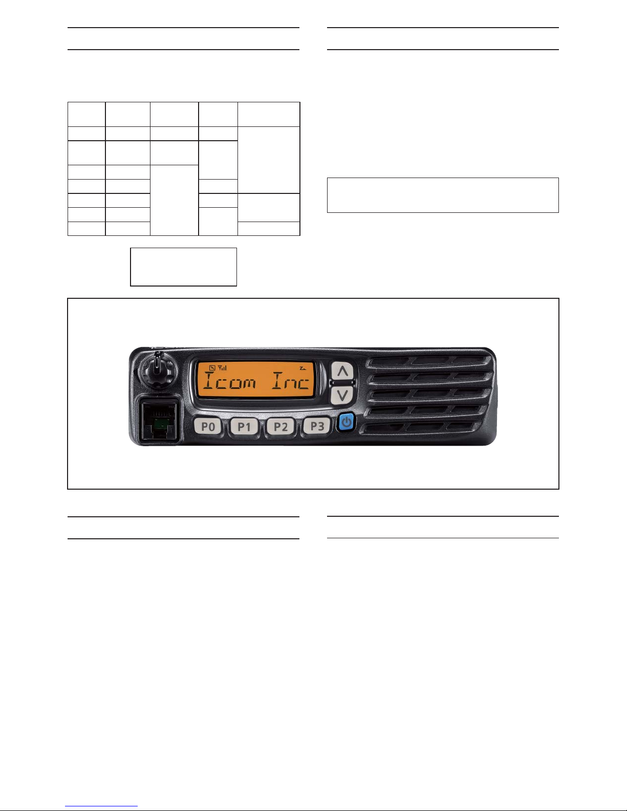
TABLE OF CONTENTS
SECTION 1 SPECIFICATIONS
SECTION 2 INSIDE VIEWS
SECTION 3 DISASSEMBLY INSTRUCTION
SECTION 4 OPTIONAL UNIT INSTALLATION
SECTION 5 CIRCUIT DESCRIPITON
5-1 RECEIVER CIRCUITS. . . . . . . . . . . . . . . . . . . . . . . . . . . . . . . . . . . . . . . . . . . . . . . . . . . . . . . . 5-1
5-2 TRANSMITTER CIRCUITS . . . . . . . . . . . . . . . . . . . . . . . . . . . . . . . . . . . . . . . . . . . . . . . . . . . . 5-3
5-3 FREQUENCY SYNTHESIZER CIRCUITS . . . . . . . . . . . . . . . . . . . . . . . . . . . . . . . . . . . . . . . . 5-4
5-4 VOLTAGE DIAGRAM . . . . . . . . . . . . . . . . . . . . . . . . . . . . . . . . . . . . . . . . . . . . . . . . . . . . . . . . . 5-4
5-5 PORT ALLOCATIONS . . . . . . . . . . . . . . . . . . . . . . . . . . . . . . . . . . . . . . . . . . . . . . . . . . . . . . . . 5-5
SECTION 6 ADJUSTMENT PROCEDURE
6-1 PREPARATION . . . . . . . . . . . . . . . . . . . . . . . . . . . . . . . . . . . . . . . . . . . . . . . . . . . . . . . . . . . . . 6-1
6-2 FREQUENCY ADJUSTMENT . . . . . . . . . . . . . . . . . . . . . . . . . . . . . . . . . . . . . . . . . . . . . . . . . . 6-4
6-3 TRANSMIT ADJUSTMENT . . . . . . . . . . . . . . . . . . . . . . . . . . . . . . . . . . . . . . . . . . . . . . . . . . . . 6-5
6-4 RECEIVE ADJUSTMENT . . . . . . . . . . . . . . . . . . . . . . . . . . . . . . . . . . . . . . . . . . . . . . . . . . . . . 6-6
SECTION 7 PARTS LIST
SECTION 8 MECHANICAL PARTS
SECTION 9 BOARD LAYOUTS
SECTION 10 GENERAL WIRING
SECTION 11 BLOCK DIAGRAM
SECTION 12 VOLTAGE DIAGRAM

1 - 1
SECTION 1
.
SPECIFICATIONS
[USA], [RUS], [CHN], [EXP] [EUR]
GENERAL
• Frequency coverage 136–174 MHz [USA], [CHN], [EXP]
146–174 MHz [RUS] 136–174 MHz
• Type of emission Wide 16K0F3E (25.0 kHz)
Middle – 14K0F3E (20.0 kHz)
Narrow 11K0F3E (12.5 kHz) 8K50F3E (12.5 kHz)
• Number of programable channels 128 channels (8 zones)
• Antenna impedance 50 Ω(nominal)
• Operating temperature range –30˚C to +60˚C (−22˚F to +140˚F) –25˚C to +55˚C
• Power supply requirement (nominal) 13.6 V DC (Negative ground) 13.2 V DC (Negative ground)
• Current drain
(approx.) RX Stand-by 300 mA
Max.audio 1200 mA
TX at 25 W 7.0 A
at 50 W 14.0 A
• Dimensions
(projections not included)
[25 W ver.] 150 (W) × 40 (H) × 117.5 (D) mm; (5 29/32 (W) × 1 9/16 (H) × 4 5/8(D) in)
[50 W ver.] 150 (W) × 40 (H) × 167.5 (D) mm;
(5 29/32 (W) × 1 9/16 (H) × 6 19/32 (D) in) –
• Weight [25 W ver.] 0.8 kg (1 3/4Ib) 0.8 kg
[50 W ver.] 1.1 kg (2 7/16 Ib) –
TRANSMITTER
• Transmit output power [25 W ver.] 25 W (High), 10 W (Low2), 2.5 W (Low1)
[50 W ver.] 50 W (High), 25 W (Low2), 5.0 W (Low1) –
• Modulation Variable reactance frequency modulation
• Max. permissible deviation Wide ±5.0 kHz
Middle – ±4.0 kHz
Narrow ±2.5 kHz
• Frequency error ±2.5 ppm ±1.5 kHz
• Spurious emission 70 dB typ. 0.25 μW (≤1 GHz), 1.0 μW (>1 GHz)
• Adjacent channel power Wide 70 dB min.
Middle – 70 dB min.
Narrow 60 dB min.
• Audio frequency response +1 dB to –3 dB of 6 dB/octave (from 500–2500 Hz)
• Audio harmonic distortion 3% typ. (with 1 kHz AF 40% deviation)
• FM hum and noise
(without CCITT filter)
Wide More than 40 dB (46 dB typ.) –
Narrow More than 34 dB (40 dB typ.) –
• Residual modulation
(with CCITT filter)
Wide – More than 45 dB (55 dB typ.)
Middle – More than 43 dB (53 dB typ.)
Narrow – More than 40 dB (50 dB typ.)
• Limiting charact of modulation 70–100% of max. deviation
• Microphone impedance 600 Ω

1 - 2
[USA], [RUS], [CHN], [EXP] [EUR]
RECEIVER
• Receive system Double-conversion superheterodyne
• Intermediate frequencies 1st IF; 46.35 MHz, 2nd IF; 450 kHz
• Sensitivity 0.25 μV typ. at 12 dB SINAD −4 dBμV (EMF) typ. at 20 dB SINAD
• Squelch sensitivity (at threshold) 0.25 μV typ. −4 dBμV (EMF) typ.
• Adjacent channel
selectivity
Wide More than 70 dB (75 dB typ.) Other than [RUS]
82 dB typ. [RUS]
Middle − More than 70 dB (75 dB typ.)
Narrow More than 60 dB (65 dB typ.)
• Spurious response 70 dB min.
• Intermodulation More than 70 dB (75 dB typ.) More than 65 dB (67 dB typ.)
• FM hum and noise
(without CCITT filter)
Wide More than 40 dB (45 dB typ.) –
Narrow More than 34 dB (40 dB typ.) –
• Residual modulation
(with CCITT filter)
Wide – More than 45 dB (55 dB typ.)
Middle – More than 43 dB (53 dB typ.)
Narrow – More than 40 dB (50 dB typ.)
• Audio output power 4.0 W typ. at 5% distortion with a 4 Ωload
• Audio output impedance 4 Ω

2 - 1
SECTION 2
.
INSIDE VIEWS
• FRONT UNIT
(TOP VIEW)
CPU
(IC1)
LCD DRIVER
(IC6)
TONE LPF
(IC5)
TONE FILTER SWITCH
(Q3)
EEPROM
(IC3)
CLOCK FREQUENCY
SHIFT DIODE
(D6)
BACKLIGHT CONTROLLER
(Q5)
DIMMER CONTROLLER
(Q2)
BACKLIGHT DRIVER
(Q1)
RESET IC
(IC2)

2 - 2
• MAIN-A UNIT
(TOP VIEW)
IF IC
(IC1)
LPF
(Q39)
PLL IC
(IC4)
CPU5 LINE REGULATOR
(IC10)
RIPPLE FILTER
(Q17)
VCO SWITCH
(Q15)
POWER SWITCH
(Q23)
+8 REGULATOR
(IC9)
LOCK VOLATGE BUFFER
(Q18)
WIDE/NARROW
PHASE SHIFTER SWITCH
(Q5)
R8 REGULATOR
(Q30)
POWER SWITCH
(Q24)
APC AMP
(IC2)
WIDE/NARROW
2ND IF FILTER SWITCH
(Q40)
1ST IF FILTER
(FI1)

2 - 3
VCO
• MAIN-A UNIT
(BOTTOM VIEW)
AF/TONE FILTER
(IC16)
AF POWER AMP
(IC8)
AF MUTE SWITCH
(Q35, Q36)
Ext. MODULATION
LINE SWITCH
(Q31)
REFERENCE FREQUENCY
OSCILLATOR (X2)
REFERENCE OSCILLATOR
MODULATION AMP
(IC19)
D/A CONVERTER
(IC18)
AF PRE-AMP
(IC15)
EXPANDER
(IC17)
ANALOG SWITCH
(IC14)
D/A CONVERTER
(IC20)
DRIVE AMP
(Q9)
RF AMP
(Q9)
1ST MIXER
(Q3)
2ND IF FILTER
(FI2)
2ND IF FILTER
(FI6)
+5V REGULATOR
(Q27,Q28) T8 REGULATOR
(Q25)

3 - 1
SECTION 3
.
DISASSEMBLY INSTRUCTION
FLAT
CABLE
TOP COVER
FRONT PANEL
SPEAKER
CABLE
MAIN UNIT
UNSOLDER
Solder
remover
MAIN UNIT
MAIN UNIT
1) Unscrew 4 screws from the top cover, and remove the top
cover.
2) Disconnect the flat cable and speaker cable.
3) Unscrew 2 screws from the both sides, and remove the
front panel in the direction of the arrow.
5) Unscrew 9 screws from the MAIN UNIT.
6) Unsolder total of 9 points; 3 points at the antenna
connector, 6 points at the PA module.
7) Take off the MAIN UNIT from the CHASSIS.

4 - 1
SECTION 4 OPTIONAL PRODUCTS INSTALLATION
Install optional UT-108 as follows;
1) Turn the transceiver OFF, then disconnect the DC cable.
2) Unscrew 4 screws, then remove the bottom cover.
3) Install the unit as shown below.
4) Recover the bottom cover, screws and DC power cable.
Install optional OPC-1939 as follows;
1) Turn the transceiver OFF, then disconnect the DC power
cable.
2) Unscrew 4 screws, then remove the bottom cover.
3) Install the cable as shown below.
Install optional UT-109R or UT-110R as follows;
1) Turn the transceiver OFF, then disconnect the DC power
cable.
2) Unscrew 4 screws, then remove the bottom cover.
3) Cut the pattern on the PCB at "MIC" and "DISC" as
showon below.
4) Install the unit as shown below.
5) Recover the bottom cover, screws and DC power cable.
OPC-1939
Cut off the bushing as in the illustration,
when you install the optional OPC-1939.
K
I
MIC
DISC
4) Cut or short the patterns as below. (For AF output)
6) Recover the bottom cover, screws and DC power cable.
NOTE: Be sure to recover the patterns when you remove the optional product. Otherwise no TX modulation or AF output is available.
Solder
remover
D
5) Short the pattern as below. (For modulation input)

5 - 1
1ST IF CIRCUITS
The RX signals from the BPF are mixed with the 1st LO
signals to be converted into the 46.35 MHz 1st IF signal.
The 1st LO signals are generated by the RX VCO (Q14,
D33, D34, L26, L39, etc.), and passed through the LO SW
(D15) and attenuator, then applied to the 1st mixer (Q3)
The converted 1st IF signal is filtered by the crystal filter (FI1)
and amplified by the 1st IF AMP (Q4), then applied to the IF
IC (IC1).
5-1 RECEIVER CIRCUITS
RF CIRCUITS
RF signals from the antenna are passed through the LPF (as
the harmonic filter for transmitting) and antenna SW, then
applied to the RX BPF circuit.
The applied RX signals are passed through the 2-staged
tuned BPF (D4, D8) to remove unwanted out-of-band
signals, and amplified by the low-noise RF AMP (Q2), then
applied to the 1st mixer (Q3) via another 2-staged tuned
BPF (D9, 10).
Total of 4 stage BPF are tuned to the RX frequency by the
tuning voltage “T1” and “T2” from the D/A converter (IC20),
to obtain required IMD characteristic.
2ND IF AND DEMODULATOR CIRCUITS
The amplified 1st IF signal is mixed with the 2nd LO signal
at the internal 2nd IF mixer of the IF IC (IC1), to obtain the
450 kHz 2nd IF signal.
The 15.3 MHz signal generated by the reference oscillator
(X2) is passed through the filter AMP (Q34, L33, 35, C305–
308) to extract the 45.9 MHz 3rd harmonic component. The
45.9 MHz signal is then applied to pin 2 of IF IC (IC1) as
the 2nd LO signal.
The converted 2nd IF signal is output from pin 3 of IF IC
(IC1), and filtered by the ceramic filters (FI2 and FI6 for
Narrow mode; FI2 only for Wide mode) to remove unwanted
out-of-band signals, then applied to the internal frequency-
demodulator of IF IC (IC1) from pin 5.
The demodulator is a quadrature type which uses X1 as the
phase shifter.
The frequency-demodulated AF signals are output from pin 9
to AF circuits.
• RF CIRCUITS
• 2ND IF AND DEMODULATORCIRCUITS
• 1ST IF CIRCUITS
SECTION 5
.
CIRCUIT DESCRIPTION
LPFLP F PWR
DET
D1,D11
ANT
SW
D2,3,5,6,48
BPF
D10
BPF
D9
BPF
D4
BPF
D8
RF
AMP
Q2
AGC
Q1
Tuning voltage “T2”
To 1st IF circuits
Tuning voltage “T1”
136-174 MHz
RSSI
From the TX AMP
TX/RX
SW
D15
Q3
1st mixer
BPF
XTAL
FI1
IF
AMP
Q4
LPF
From RF circuits
To IF IC 46.35 MHz
1st LO signals
(182.35 MHz-220.35 MHz)
REF X2
X3 Q34
X1
BPF
BPF
CERAMIC
FI6
W/N
SW
Q5
BPF
CERAMIC
FI2
W/N
SW
D56
Q40
W/N
SW
D57
D/A
IF IC
From 1st IF circuits
IC1:TA31136FN
IC18
AK2330
NWC
15.3MHz
45.9MHz
DISC
SQIN
450kHz
To the AF circuits
NWC

5 - 2
• RX AF CIRCUITS
AF CIRCUITS
The demodulated AF signals from the IF IC (IC1) are
amplified and filtered by the HPF (IC16), and passed
through the AF line SW (IC14) and LPF (IC16). The filtered
AF signals are adjusted its level (=loudness) by the D/A
converter (IC18), and applied to the AF AMP (IC15) via the
AF line SW (IC14).
The amplified AF signals are applied to the AF power AMP
(IC8) and power-amplified to obtain AF output level.
The power-amplified AF signals are applied to the internal
speaker on the FRONT UNIT or output from the external
speaker jack on the rear panel.
SIGNALING (DECODING)
Demodulated signals from pin 9 of the IF IC (IC1) are
passed through the LPF to extract tone signals contained in
the demodulated signals.
2/5 tone signals are extracted by the LPF (IC16). CTCSS/
DTCS signals are extracted by the LPF (Q39).
These extracted tone signals are applied to the CPU (FRONT
UNIT: IC1) for decoding.
LPF
IC16
LPF
IC16
LPF
Q39
HPF
IC16
AF
AMP
IC15 AF
POWER
AMP IC8
LA4425A
AF
MUTE
Q35,36,D29
Int. speaker
Ext. speaker jack
J4
ANALOG
SW
SDEC
To CPU (FRONT UNIT: IC1)
CDEC
IC14
CD4066
D/A
IC18
AK2330
(2/5 TONE signals)
(TCSS/DTCS signals)
FRONT UNIT
AF ON
DISC
From the IF IC
DISC
DISC
VRAF TMONI
RXAF

• TX AF CIRCUITS
• MODULATION CIRCUITS
• TX AMPLIFIERS APC CIRCUIT
5 - 3
5-2 TRANSMITTER CIRCUITS
MIC AMPLIFIER (FRONT UNIT)
Audio signals from the connected microphone are applied to
the MIC AMP (IC5) via the microphone connector (J1). The
amplified MIC signals are applied to the MAIN UNIT.
TX AF CIRCUITS
The MIC signals from the FRONT UNIT are passed through
the D/A converter (as a MIC gain controller; IC18) for level
adjustment, and applied to the limiter AMP which is also
rolled to the pre-emphasis circuit (IC16).
MIC MUTE SWITCH
The pre-emphasized MIC signals are passed through the
MIC mute SW (IC14).
While receiving, the MIC mute SW (IC14) cuts the MIC line
off, and is controlled by “MMUT” signal from the expander
(IC17).
SPLATTER FILTER
The MIC signals from the MIC mute SW (IC14) are applied
to the splatter filter (IC16).
The splatter filter (IC16) is also used as the AF Summing
AMP for tone signals modulation (CTCSS, 2/5 TONE).
MODULATION CIRCUIT
MIC signals from the splatter filter (IC16) is level-adjusted
(=deviation adjustment) by the D/A converter (IC18), and
applied to the TX VCO (Q13, D16, 31) via modulation mute
SW (IC14) as the modulation signals.
The MIC signals are also applied to the reference frequency
oscillator (X2) as the modulation signals via D/A converter
(IC18) and REF AMP (IC19).
CTCSS/DTCS SIGNALS ENCODING (FRONT UNIT)
The CTCSS/DTCS encoding signals from the CPU (IC1)
“CENC0–CENC2” are passed through the LPF (IC5) for
waveform conversion, and applied to the MAIN UNIT as tone
modulation signals.
2/5 TONE, DTMF ENCODING (FRONT UNIT)
Encoding signal from the CPU (IC1) named “SENC” is
passed through the LPF (IC5), and applied to the MAIN
UNIT as tone modulation signals.
TX AMPLIFIERS
The frequency-modulated signal from the TX VCO is buffer-
amplified by two buffers (Q11 and Q10), and applied to the
drive AMP (Q9) as the TX signal via the LO SW (D14). The
amplified TX signal is applied to the FET HPA module (IC3)
via the LPF, and power-amplified to obtain TX output power
level.
The power-amplified TX signal is passed through the
antenna SW (D3) and LPF as a harmonic filter, then fed to
the antenna.
APC CIRCUIT
A portion of TX signal rectified by D1, D11 and D12 on the
TX line to detect TX power level. The rectified voltage is
applied to the APC AMP (IC2), and the APC AMP controls
the gain of HPA module (IC3) automatically by comparing
the rectified voltage and the power setting voltage "T1."
Splat.
IC16
Limiter
Pre-empha.
IC16
AMP
IC5
HPF MIC
line
SW
MIC
D/A
IC14
CD4066
IC18
A K2330
MICROPHONE
CONNECTOR
J1
FRONT UNIT
MIC
BAL
To the Reference
frequency oscillator
MODI
MCOT
MCGO
TONE
CDTS
MODVRAF
TX VCO
SPIN
REF
OSC
X2
CR-794
TX/RX
SW
D14,D15
Q13,D16,31
FIL
LOOPPLL
IC
IC4
MB15A02
FM
MOD
D18
BUFF
Q10
BUFF
Q11
IC19
AMP
REF
TX VCO
BAL
15.3 MHz
From the D/A converter From the MIC line SW
To TX AMPs
LV
LPFLPF LP FLP F PWR
DET
D11,D12
MUTE
SW
D28
ANT
SW
D3
PWR
AMP
IC
RX circuits
3
APC
AMP
IC2
DRIVE
AMP
Q8
T1 TMUT
136-174 MHz
From TX VCO

5 - 4
5-3 FREQUENCY SYNTHSIZER CIRCUITS
VCOs
The TX VCO which generates TX signal is composed
by Q13, D16, D31, L25, L38, etc., and the frequency
modulation is carried out by applying modulation signals to
D18.
The RX VCO which generates 1st LO signals is composed
by Q14, D33, D34, L26, L39, etc.
These two VCOs are switched by the VCO SW (Q15, 16)
using “RXC” signal.
The output signals from each VCO are amplified by the
buffer AMP (Q11) and LO AMP (Q10), then applied to the
TX or RX circuits.
A portion of oscllated signals is applied to the PLL IC (IC4)
via buffer AMP (Q12).
PLL
The applied VCO output is divided according to the serial
data including divide ratio from the CPU, at the prescaler
and programmable divider. In the same way, the reference
frequency signal from the reference frequency signal
oscillator is applied to the PLL IC and divide so that these
are the same frequency.
The frequency-matched signals are applied to the phase
comparator and phase-compared. The resulted phase
difference is detected as a phase-type signal, and level-
adjusted at the charge pump then output. The output pulse
type signal is passed through the loop filter to be converted
into the DC voltage (=Lock Voltage).
Applying the lock voltage to the variable capacitors
(VD) which composes a part of the resonator of VCO,
the capacitance of VDs changes corresponding to the
applied lock voltage. This causes the change of resonation
frequency that determines the VCO oscillating frequency to
keep the VCO frequency constant.
When the oscillation frequency drifts, its phase changes
from that of the reference frequency, causing a lock voltage
change to compensate for the drift in the VCO oscillating
frequency.
• FREQUENCY SYNTHESIZER CIRCUITS
5-4 VOLTAGE DIAGRAM
Voltage from the power supply is routed to the whole of the transceiver via regulators and switches.
LPF
REF
X2
CR-794
TX/RX
SW
D14,D15
Q14,D33,34
Q13,D16,31
FIL
RIPPLE
Q17
VCO
SW
Q15,16
FIL
LOOPPLL
IC
IC4
MB15A02
X3
Q34
FM
MOD
D18
BPF
BUFF
Q10
BUFF
Q11
LPF
IC19
AMP
X2
Q12
BPF
D54,55
TLV
AD J
D53
RLV
AD J
D52
IF IC
8V
RXC
RX VCO
TX VCO
IC1:TA31136FN
REF 15.3MHz
Clock,Data,Strobe
45.9MHz
182.35 MHz-220.35 MHz
136/146 MHz-1740 MHz
TXC
T8V
RLVA
TLVA
LVLV
SW
POWER
Q23 Q24
+5
5V
REG
Q27 Q28
+8
REG
IC9
T8
REG
Q25 Q29
D23
W2
Power supply cable
REG
CPU5
IC10
Q26 Q30
R8
REG
Driver(Q9), APC AMP(IC2), etc.
IF IC (IC1), PLL IC(IC4), etc.
RF AMP(Q2), 1st IF AMP(Q4), 1st mixer(Q3), etc.
External output(from J6)
VCOs, FRONT UNIT
T8V
R8V
8V
VCC
TMUT
RXC
PWON
HV
CPU5CPU5
VCC
8V
8V
8V
HPA module(IC3)
HV

5 - 5
5-5-1 CPU (FRONT UNIT; IC1)
Pin
No.
Port
Name Description
1−3 KR1−
KR3 Input ports for dealer-programmable keys.
4−8 KS0−
KS4 Output ports for dealer-programmable keys.
10 CCS Outputs chip-select signal to the attached optional
unit.
19−
21
CENC0−
CENC2 Output ports for CTCSS/DTCS signal.
23 DUSE
Frequency response of tone filter (FRONT UNIT;
IC5) switching signal.
“Low”=While transmitting.
24 IPTT PTT input from connected microphone.
“Low”=PTT is pushed.
25 HANG Microphone on/off hook detect.
“Low”=The microphone is off hook.
30 PLST Outputs PLL strobe signal to the PLL IC (MAIN UNIT;
IC4, pin 11).
34 ULCK
Input port for PLL unlock detect signal from the
PLL IC (MAIN UNIT; IC4, pin 7).
“Low”=While the PLL circuit is unlocked.
39 DSDA Outputs serial data to the D/A converter (MAIN
UNIT; IC20, pin 6).
43 SENC Outputs DTMF signals to the LPF (FRONT UNIT;
IC5, pin 3).
44 BEEP Outputs beep sounds to the LPF (FRONT UNIT;
IC5, pin 7).
45 SDEC Input port for DTMF signals.
46 CDEC Input port for CTCSS/DTCS signals.
48 BATV Input port for power supply voltage.
49 LVIN Input port for VCO lock voltage.
50 RSSI Input port for receive signal strength level signal
from the IF IC (MAIN UNIT; IC1, pin 12).
51 TEMP Voltage divided by thermal register (MAIN UNIT;
R209) and R210. (temperature monitor)
52 AFVI [VOL] dial (FRONT UNIT; R14) input. (divided
voltage of 5V line)
59 RES
Input port for CPU reset signal from the reset IC
(FRONT UNIT; IC8, pin 1).
“Low”=When the CPU is reset.
69 CSFT Outputs CPU clock shift signal to the clock
frequency shift switch (FRONT UNIT; D6).
71 DAST Outputs strobe signal to the D/A converter (MAIN
UNIT; IC18, pin 7).
72 IGSW/
DIM
• Ignition SW control input.
Or
• Dimmer control input.
75 NOIS
Input port for noise signal from the IF IC (
MAIN UNIT;
IC1, pin 13).
79 CLO Cloning data output.
80 CLI Cloning data input.
82 ESDA Outputs serial data to the EEPROM (FRONT UNIT;
IC3, pin 5).
85 ESCL Outputs clock signal to the EEPROM (FRONT
UNIT; IC3, pin 6).
86 PWON Transceiver's power control.
“High”=Power ON.
91 LSO Outputs serial data to the LCD driver (FRONT UNIT;
IC6, pin 48).
92 LSCK Outputs clock signal to the LCD driver (FRONT UNIT;
IC6, pin 47).
93 LCS Outputs chip-enable signal to the LCD driver
(FRONT UNIT; IC6, pin 46).
94 LINH Outputs display inhibit signal to the LCD driver
(FRONT UNIT; IC6, pin 45).
95 LIGT2
Outputs LCD backlight control signal to the
backlight LEDs (FRONT UNIT; DS1–9) driver
(FRONT UNIT; Q5).
“High”=While the backlight is ON.
Pin
No.
Port
Name Description
98 SCK
Outputs serial clock signal to the PLL IC (IC4, pin
9) and D/A converters (IC17, pin 3/IC18, pin 8/
IC20, pin 7).
99 SO Outputs serial data to the PLL IC (IC4, pin 9) and D/
A converters (IC17, pin 3/IC18, pin 8/IC20, pin 7).
100 KR0 Input ports for dealer-programmable keys.
5-5-2 EXPANDER (MAIN UNIT; IC17)
Pin
No.
Line
Name Description
1 EXST Strobe (load enable) input.
2 SO Serial data input.
3 SCK Serial clock input.
4 RXC T8V, R8V lines and RX VCO ON/OFF control.
5 AFON AF mute SW (Q35) control.
“Low”=Mute
6 NWC
• RX band width switching signal to the 2nd IF
filter SW (D56, 57).
“Low”=Narrow mode
• RX band width switching signal to the phase
shifter SW (Q5).
“Low”=Wide mode
7 RMUT
Outputs AF mute signal to the analog switch
(IC3, pins 12, 13).
“Low”=While the squelch is close or transmitting.
12 HORNO External device control.
“Low”=Pin 6 of OPC-1939 (if connected) is “Low.”
13 TMUT
Outputs transmit mute signal to the transmit
mute switch (Q46).
“High”=Transmitting is muted.
5-5-3 D/A CONVERTER (MAIN UNIT; IC18)
Pin
No. Description
2, 3 MIC signal level adjustment.
4, 5 RX AF/MIC signal level adjustment.
16, 17 Tone signal level adjustment.
18, 19 Oscillation frequency control voltage to the reference
frequency oscillator (X2).
20, 21 Modulation signal level adjustment.
22, 23 Beep sound loudness adjustment.
24, 25 Squelch threshold level adjustment.
5-5-4 D/A CONVERTER (MAIN UNIT; IC20)
Pin
No.
Line
Name Description
1T1
• While receiving
Tuning voltage to the tuned BPF (D4, 8).
• While transmitting
TX power level setting signal to the APC AMP
IC2).
2 T2 Tuning voltage to the tuned BPF (D9, 10).
3TLVA
Oscillation frequency correcting voltage to the TX
VCO (Q13, D16, 18, 31, 53).
4RLVA
Oscillation frequency correcting voltage to the RX
VCO (Q14, D33, 34, 52).
5-5 PORT ALLOCATIONS

6 - 1
SECTION 6
.
ADJUSTMENT PROCEDURE
EQUIPMENT GRADE AND RANGE EQUIPMENT GRADE AND RANGE
Cloning Software CS-F5020 : Revision 1.0 or later JIG Cable Modified OPC-1122U
(see the illust below)
DC Power Supply
Output voltage
Current capacity
: 13.6 V DC except [EUR]
13.2 V DC [EUR]
: More than 20 A
Attenuator
Power attenuation
Capacity
: 40 or 50 dB
: 30 W [25 W ver.]
60 W [50 W ver.]
Modulation
Analyzer
Frequency range
Measuring range
: DC–300 MHz
: 0 to ±10 kHz External Speaker Input impedance
Capacity
: 4 Ω
: 20 W or more
Frequency Counter
Frequency range
Frequency accuracy
Sensitivity
: 0.1–300 MHz
: ±1 ppm or better
: 100 mV or better
Standard Signal
Generator (SSG)
Frequency range
Output level
: 0.1–300 MHz
: 0.1 µV to 32 mV
(–127 to –17 dBm)
RF Power Meter
Measuring range
Frequency range
Impedance
SWR
: 0.1–30 W [25 W ver.]
0.1–60 W [50 W ver.]
: 100–300 MHz
: 50 Ω
: Better than 1.2 : 1
Oscilloscope Frequency rang
Measuring range
: DC–20 MHz
: 0.01–20 V
6-1 PREPARATION
MREQUIRED EQUIPMENTS
MJIG CABLE
Add a jumper wire here
OPC-1122U (USB type Cloning cable)
+
GND
MIC
PTT
GND
GND
SP
PTT SWITCH
+−
AC MILLIVOLTMETER
(10 mV to 10 V)
AUDIO GENERATOR
(300–3000 Hz/1–500 mV)
+−
+−
4.7 µF
EXT. SPEAKER
(5 W/4 Ω)
SETTING;
Frequency : 1 kHz
Level : 40 mVrms
Waveform : Sine wave

6 - 2
MADJUSTMENT FREQUENCIES
Before starting adjustment, clone adjustment frequencies and settings into the transceiver as below.
• For except [F5026]
• For [F5026]
Select “Middle”
NOTE: FOR [F5022], when adjust “Deviation,” “Modulation Balance,” “RX SENSITIVITY”
and “S-meter” in the middle band, change the bandwidth to “Middle” as below.

6 - 3
MADJUSTMENT UTILITY WINDOW (example)
MCONNECTION
Modulation analyzer
(DC measurable)
Attenuator
40 dB or 50 dB
to the antenna connector
to DC cable
Standard signal generator
–127 to –17 dBm
(0.1 V to 32 mV)
CAUTION:
DO NOT transmit while
SSG is connected to
the antenna connector.
RF power meter
30 W [25 W ver.]
60 W [50 W ver.]
DC power supply
13.6 V / 20 A except [EUR]
13.2 V / 20 A [EUR]
Frequency
counter
Oscilloscope
AC millivoltmeter
Audio generator
to the MIC
connector
JIG CABLE
to USB port
PC
TX POWER
MOD. BALANCE
DEVIATION
CTCSS\DTCS
SQUELCH
REF. FREQUENCY
RX SENSITIVITY
LOCK VOLTAGE
RSSI
(S3 and S1 level)
ADJ. CHANNEL
Click to open the
“I/O Check window”

6 - 4
6-2 FREQUENCY ADJUSTMENT
1) Select an adjustment item using cursor or [↑] / [↓] keys of the PC’s keyboard.
2) Set or modify the adjustment value as specified using [←] / [→] keys of the PC’s keyboard, then push the [ENTER] key.
ADJUSTMENT ADJUSTMENT CONDITION OPERatio VALUE
PLL LOCK
VOLTAGE
-adjustment-
[RX LVA]
1 • Channel
• Receiving
: 1-1 Select the item [RX LVA], then adjust the
voltage (LVIN) using [←] / [→] keys of the
PC’s keyboard.
1.1 V
Other than
[F5026], [F5026H]
1.7 V
[F5026], [F5026H]
[TX LVA] 2 • Channel
• Transmitting
: 1-1 Select the item [TX LVA], then adjust the
voltage (LVIN) using [←] / [→] keys of the
PC’s keyboard.
1.06 V
Other than
[F5026], [F5026H]
1.4 V
[F5026], [F5026H]
PLL LOCK
VOLTAGE
-verification-
1 • Channel
• Receiving
: 1-2 Click [Reload (F5)] button, then check the
“LVIN” item on the “I/O Check window.”
3.0–4.0 V
2 • Channel
• Transmitting
: 1-2 2.5–3.5 V
REFERENCE
FREQUENCY
[REF]
1 • Channel : 1-3
• Connect an RF power meter to the
antenna connector.
• Transmitting
Loosely couple a frequency counter to the
antenna connector.
174.000000 MHz
Lock voltage
• I/O Check window
(The values shown in the above screen are example only.
Each transceiver has their own values.)

6 - 5
6-3 TRANSMIT ADJUSTMENT
1) Select an adjustment item using cursor or [↑] / [↓] keys of the PC’s keyboard.
2) Set or modify the adjustment value as specified using [←] / [→] keys of the PC’s keyboard, then push the [ENTER] key.
ADJUSTMENT ADJUSTMENT CONDITION OPERatio VALUE
OUTPUT
POWER
[Power (Hi)]
1 • Channel : 1-4
• Transmitting
Connect an RF power meter to the an-
tenna connector.
25 W
[25W ver.]
50 W
[50 W ver.]
[Power (L2)] 2 • Channel : 1-5
• Transmitting
10 W
[25W ver.]
25 W
[50 W ver.]
[Power (L1)] 3 • Channel : 1-6
• Transmitting
2.5 W
[25W ver.]
5.0 W
[50 W ver.]
MODULATION
BALANCE
[BAL]
1 • Channel : 1-7
• No audio signals applied to the JIG cable.
• Set a modulation analyzer as;
HPF : OFF
LPF : 20 kHz
De-emphasis : OFF
Detector : (P–P)/2
• Transmitting.
Connect the Modulation Analyzer with
an oscilloscope to the antenna connec-
tor through an attenuator.
Set to square
waveform
DEVIATION
-PREPARA-
TION-
1• Connect an audio generator to the JIG
cable and set as;
Frequency : 1.0 kHz
Level : 40 mVrms
• Set the modulation analyzer to the
same condition as “MODULATION BAL-
ANCE.”
Connect a Modulation Analyzer with an
oscilloscope to the antenna connector
through an attenuator.
–
(NARROW)
[MOD N]
2• Channel : 1-8
• Transmitting ±2.05 to ±2.15 kHz
(WIDE)
[MOD Ratio]
3• Channel : 1-9
• Transmitting
±4.05 to ±4.15 kHz
(MIDDLE)*
[MOD Ratio]
4• Channel : 1-10
• Transmitting
±3.25 to ±3.35 kHz
CTCSS/DTCS
DEVIATION
[CTCSS/DTCS]
1• Channel : 1-11
• No audio signals applied to the JIG cable.
• Set the Modulation Analyzer to the
same condition as “MODULATION BAL-
ANCE.”
• Transmitting
Connect a Modulation Analyzer with an
oscilloscope to the antenna connector
through an attenuator.
±0.65 to ±0.75 kHz
*: [EUR] only
Other manuals for ic-f5021
1
This manual suits for next models
6
Table of contents
Other Icom Transceiver manuals

Icom
Icom IC-92AD User manual

Icom
Icom IC-M33 User manual

Icom
Icom IC-M423 User manual

Icom
Icom IC-756PROIII Quick start guide

Icom
Icom IC-726 User manual

Icom
Icom IC-F3210D Series User manual

Icom
Icom IC-12GAT User manual

Icom
Icom iF3102D User manual

Icom
Icom IC-80AD User manual

Icom
Icom IC-F4GT Building instructions