IDT 82P33731 User manual
USER GUIDE
REVISION C 09/29/14 1 ©2014 Integrated Device Technology, Inc.
82P33731/33831 Evaluation Board
Introduction
The 82P33731/33831 evaluation board is designed to help the customer evaluate the IDT82P33731 and IDT82P33831 devices.
This user guide will accomplish the following:
•Introduce the board on its power supply and jumper settings
•Describe the input and output connectors for normal operation
•How to bring up the board by using Timing Commander software GUI
•How to configure and program the board to generate standard-compliant frequencies
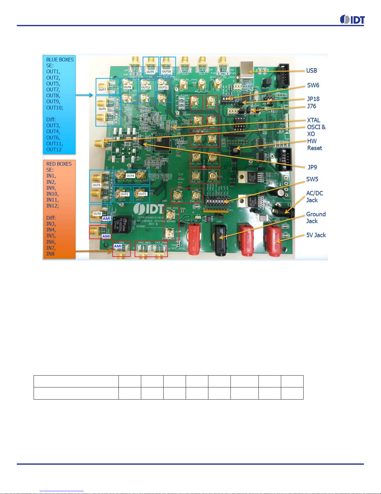
Board Overview
Use Figure 1 to identify various components of the board: Input and output SMA connectors; Power supply jacks and some
jumper settings necessary for the board operations. Detailed descriptions are as follows:
•Input SMA Connectors – There are a total of 14 inputs, of which IN1, 2 are AMI inputs; IN9, 10, 11, 12, 13, 14 are
single-ended inputs; IN3, 4, 5, 6, 7, 8 are differential inputs.
•Output SMA Connectors – There are a total of 12 outputs, of which OUT1, 2, 7, 9, 10 are single-ended outputs; OUT3, 4, 5,
6, 11, 12 are differential outputs; OUT8 is an AMI output.
•USB connector – Type-B connector for GUI communications. No power is drawn from USB connector other than to power
the FTDI USB chip.
•Dip Switch SW6 – Used to configure EEPROM write protection, master or slave selection and communication protocols
between PC/GUI and the board. For typical I2C mode, set MPU_MODE[1:0] = 00 ('I2C ON').
•J76 – This is a 2x12 pin header used to set communication mode between PC and the board. Table 1 shows how to jump the
header pairs for the intended mode. Use JP18 (described below) to set I2C mode by default.
Table 1: Jumper Setting on J76
•JP18 – By default, I2C mode will be selected with JP18 shunted (jumped).
FTDI SPI Aardvark SPI/I2C FTDI I2C Motherboard SPI/I2C FTDI UART FTDI to Aardvark
3-4 Jumper 1-3 Jumper 3-4 Jumper 3-5 Jumper 4-6 Jumper 1-2 Jumper
9-10 Jumper 7-9 Jumper 9-10 Jumper 9-11 Jumper 9-10 Jumper 7-8 Jumper
15-16 Jumper 13-15 Jumper 14-16 Jumper 15-17 Jumper 15-16 Jumper 13-14 Jumper
21-22 Jumper 19-21 Jumper 21-23 Jumper 19-20 Jumper
2 REVISION C 09/29/14
82P33731/33831 EVALUATION BOARD
Figure 1. Board Overview
•APLL3 Crystals – Crystals for APLL3 in the device. Three frequencies are supported – 24.8832MHz, 25MHz and
25.78125MHz – generating three different mode frequencies for SONET, Ethernet and Ethernet LAN, respectively. On the
board, two crystals are installed and supported at the same time.
•OSCI input and XO – System reference clock input. Refer to JP9 for clock source selection. The frequency of this input clock
is selected by XO_FREQ[2:0] pins described in SW5.
•HW Reset button – Pressing this button will reset the device to default condition.
•JP9 – 3-pin header used to select the system reference clock to be from OSCI or XO. Please see board silkscreen for source
selection.
•Dip Switch SW5 – This dip switch contains the following bit configurations:
◦System clock frequency selection – switch the 3 bits to match OSCI frequency. Default frequency is 12.8MHz.
Table 2: OSCI frequency Selections by SW5
◦SONET/SDH selection: This bit determines the value of IN_SONET_SDH during reset.
◦I2C address bits: I2C_AD[2:1] sets the lower 3-bit address of 7-bit I2C address with the least significant bit, I2C_AD0
being ignored. Higher 4 bits is fixed at 4'b1010. This only applies to I2C mode (MPU_MODE[1:0] = 00 in SW6).
•AC/DC Power Jack – Using a wall adapter AC/DC power supply (output 5VDC/3A with center-positive jack) can power the
board, if 5VDC Power Jack is not supplied with a 5VDC power source.
XO_FREQ[2:0] 000 001 010 011 100 101 110 111
Osc Frequency (MHz) 10.0 12.8 13.0 19.44 20.0 24.576 25.0 30.72

REVISION C 09/29/14 3
82P33731/33831EVALUATIONBOARD
•5VDC Power Jack – If AC/DC power source is not used, a 5VDC power source can be plugged into the jack to power the
board. Please note: Power Jacks labeled 3.3V and 1.8V are for other purposes. They can be left unused.
•5VDC Ground Jack – Paired with 5VDC Power Jack (above) to provide power return when 5VDC bench power supply is
used.
Board Power Supply
There are two ways to power up the board:
•Use an AC/DC adapter which provides 5VDC to on-board voltage regulators to generate 3.3V and 1.8V.
•Connect a 5VDC power source (i.e., a bench power supply) to the power jack that is labeled s “5V”.
There are power jacks labeled 3.3V and 1.8V. Do not use them to power the board. They are connected to the output of 3.3V
and 1.8V voltage regulators powered by either J54 or the 5VDC power jack. They can be supplied with 3.3V and 1.8V to power
the board but only if 5V is not supplied. They are used for testing purposes only; it is not recommended to use them.
USB connector is only used for communicating with the PC running Timing Commander. It is not used to provide any power
source for the board. When plugged in to PC's USB port, a green LED is lit.
Connecting the Board to PC and Power
Other than input and output cables, the only connection you need to make to operate the board is a USB cable connecting to a
PC USB port, and a power supply connection (either an AC/DC adapter or a 5VDC power source, as described above). See
Figure 2 below for different powering options.
Figure 2. Connecting the Board to the Power Supply and USB Port
4 REVISION C 09/29/14
82P33731/33831 EVALUATION BOARD
On-Board Crystal Installation
Although threecrystal frequencies (24.88320MHz, 25.00000MHz and 25.78125MHz) are supported for APLL3, only two crystals
are installed on the board. Table 3 lists the crystals with different frequencies installed on two versions of 82P33x31 evaluation
boards.
Table 3: Crystals installed on Two Versions of 82P33x31 Boards
Board Default Frequency Output
Upon power-up, the following default frequencies will be available:
•OUT1 = 25MHz
•OUT2 = 125MHz
•OUT3 = 156.25MHz
•FRSYNC = 8kHz
•MFRSYNC = 2kHz
Working with TimingCommand for Configuration
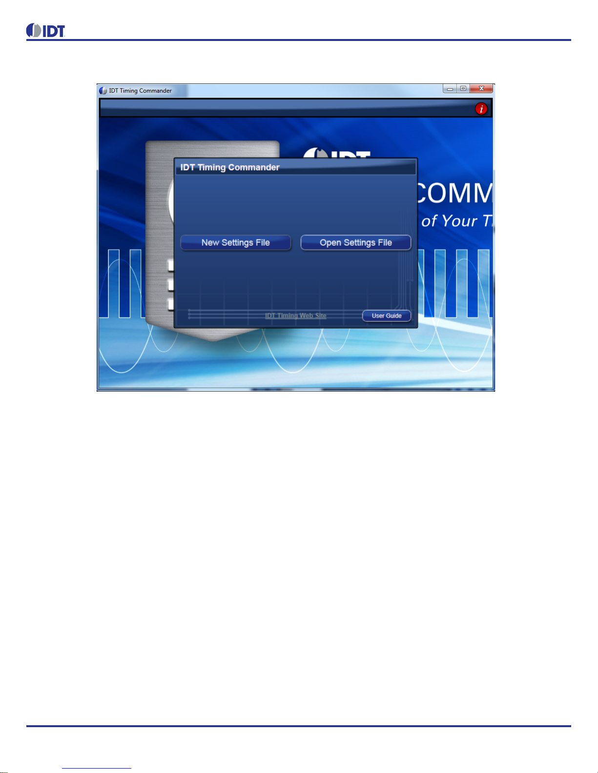
Use the following steps to start the configuration of the Timing Commander GUI and program the board using I2C:
1. Connect the board as shown in Figure 2. Press hardware reset button to reset the device. Reset is not necessary if the
board is powered up for the first time).
2. Start Timing Commander® software. You will see options of “New Setting File” and “Open Setting file”. For a new
configuration, select “New Setting File”.
EVB 12.8MHz TCXO X1 X2
82EBP33831-1 E6241LF 25.000MHz 24.576MHz
82EBP33831-2 E6241LF 24.8832MHz 25.78125MHz
REVISION C 09/29/14 5
82P33731/33831EVALUATIONBOARD
Figure 3. Starting up Timing Commander GUI
3. After selecting “New Settings File”, a device selection window will pop up. In the window, choose the intended device in
the list (82P33831 was selected in the following example). Click the button at the lower right corner of the window to
browse and select the correct personality file, then click OK.
Note: Due to the hardware structure of the chip, two personality files will need to be used to configure and program
82P33x31 board: (1) IDT82P33x31_v1.0_TC_1.5.1.2.tcp; (2) IDT82P33x31_APLL3_v1.0_TC_v1.5.1.2.tcp. To begin
with, use the personality file (1). See Figure 4 below.
Personality file (2) is used only for programming APLL3 and is deferred until Step 9 below.

6 REVISION C 09/29/14
82P33731/33831 EVALUATION BOARD
Figure 4. Select 82P33831 and Open personality file "IDT82P33x31_v1.0_TC_v1.5.1.2.tcp"
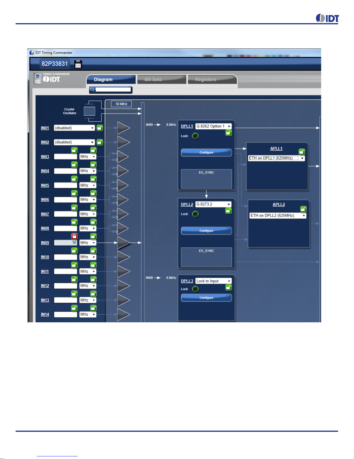
4. The GUI window with 82P33831 block diagram is open for configurations (Figure 5). Overall, the configuration window
shows 14 inputs on the left and 12 outputs are on the right side of the window. In the center of the window, DPLL1~3 and
APLL1~3 are displayed.
◦Each DPLL can be individually configured (see Step 6 below).
◦APLL1 and APLL2 each has pull-down menu to choose different base frequencies. If "Custom on DPLL" is selected, a
configuration will be needed for the associated DPLL (see Step 7 below).
◦APLL3 on the lower right corner of the window is the source for OUT11 and OUT12 only. Configuration of APLL3 is
explained in Step 7 below.
The programming of APLL3 requires a separate personality file (see Step 9) below.

REVISION C 09/29/14 7
82P33731/33831EVALUATIONBOARD
Figure 5. Top Configuration Window for 82P33831: Left – Input; Right – Output; Center – Device Block
Diagram
5. For Input configuration, most frequencies can be entered for IN01 ~ IN14 and they will be automatically configured to be
available to both DPLLs.
For each frequency entry, click outside the entry box for it to take effect. In this example, 10MHz is entered in IN09.
8 REVISION C 09/29/14
82P33731/33831 EVALUATION BOARD
Figure 6. Enter input and Output Frequencies
To associate an input clock (i.e., IN09) with a sync signal (such as 1PPS), click on the Input Buffer of IN09 (the triangle
symbol following frequency entry box), a sub-configuration window for IN09 is shown below. In the window, IN10 is
selected as sync signal.

REVISION C 09/29/14 9
82P33731/33831EVALUATIONBOARD
Figure 7. IN10 is selected as Sync Signal for IN09 (green oval)
If IN10 is only used as a sync signal for IN09, then disable IN10 to the DPLL as an input in the Input Buffer window of
IN10, shown below.
Figure 8. IN10 is disabled as an input clock to DPLL (orange oval)
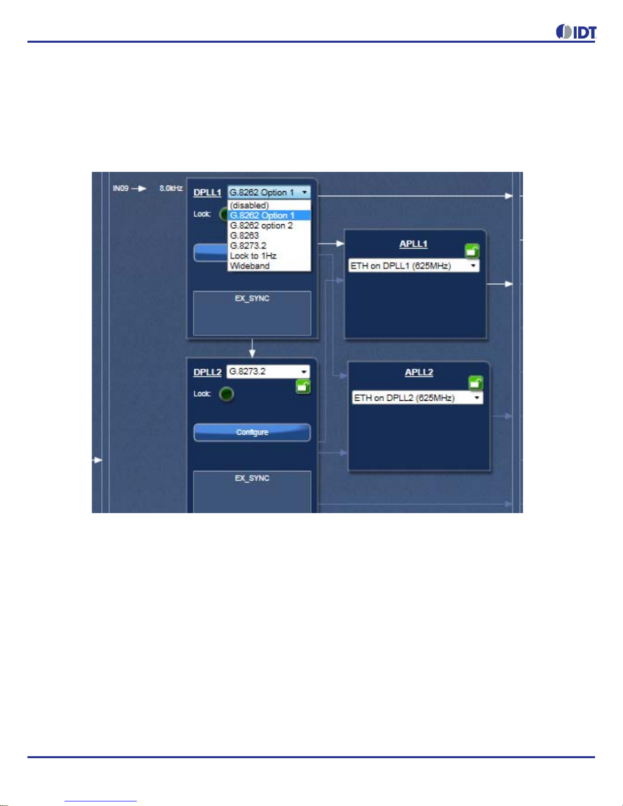
6. Each DPLL has Profile Selection and a “Configure” button. In general, the pull-down Profile Selection should be sufficient
to automatically pre-configure the DPLL and reference monitor for the specific ITU-T recommendation.
Frequency profiles selection for each DPLL from its pull-down menu include (see Figure 9 below).
◦G.8262 Option 1: to configure the DPLL for SyncE for Europe
◦G.8262 Option 2: to configure the DPLL for SyncE for NA/Japan
◦G.8263: to configure the DPLL for PEC-S-F, which occurs when typically a IEEE-1588 algorithm is controlling the
DCO with frequency offsets
10 REVISION C 09/29/14
82P33731/33831 EVALUATION BOARD
◦G.8273.2: to configure the DPLL for T-BC (Telecom Boundary Clock), which occurs when a IEEE-1588 stack is
directly controlling the DCO with phase offsets. It also puts the DPLL in combo mode to synchronize to the other PLL
running G.8262-Option 1 profile
◦Lock to 1Hz: to configure the DPLL for GPS application and locking to 1PPS only
◦Wideband: to configure the DPLL to operate in line card mode or lock to a 10MHz + 1PPS from GPS
Figure 9. Frequency Profiles for DPLL1
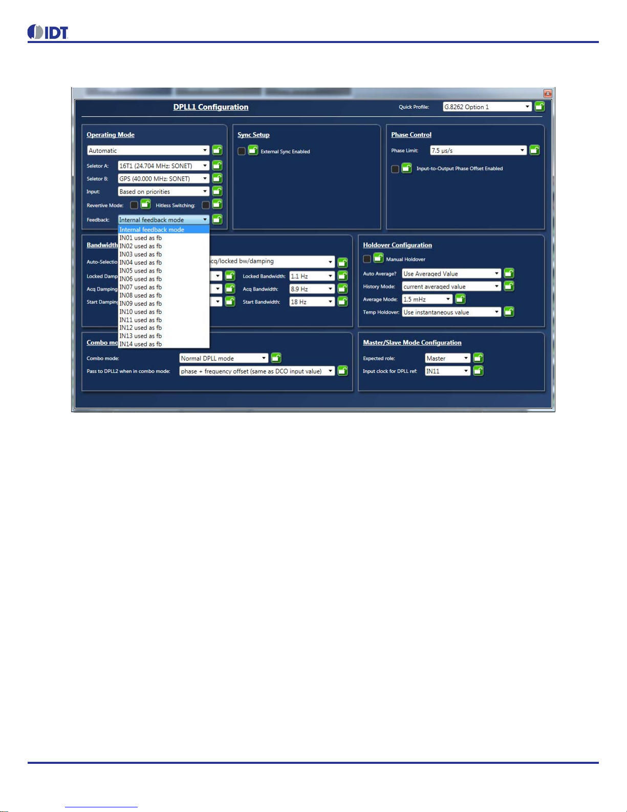
Click “Configure” button to open up configuration window for respective DPLL for additional or customized configuration.
There are pull-down items for each configuration parameter. For example, in “Operation Mode” section, you can select:
◦Automatic, or Free-up to force Lock or Free-run;
◦Different base frequencies can be selected from pull-down items in Selector A or Select B;
◦Input reference can be set manually set to a particular input, or set it in “Automatic” mode, in which case a input
reference is selected based on priority among multiple input references;
◦Feedback can be “Internal feedback mode” or use one of the input references as an “external feedback mode”. When
in external feedback mode, a clock source must be supplied to the input chosen at the same frequency as the input
to the DPLL (typically, it's 8kHz).
REVISION C 09/29/14 11
82P33731/33831EVALUATIONBOARD
Figure 10. DPLL Configuration Window - Operation Mode Settings
In “Bandwidth and Damping” section, there are two options to select DPLL's bandwidth and damping factors during start,
acquisition and locked phases:
◦Always use Locked bandwidth/damping: this option will use the bandwidth and damping factor that are available
when DPLL is locked;
◦Automatically select start/acq/locked bw/damping: preset bandwidth and damping factor values are used for the
DPLL during start, acquisition and locked phases.

12 REVISION C 09/29/14
82P33731/33831 EVALUATION BOARD
Figure 11. DPLL Configuration Window – Bandwidth/Damping Factor Settings
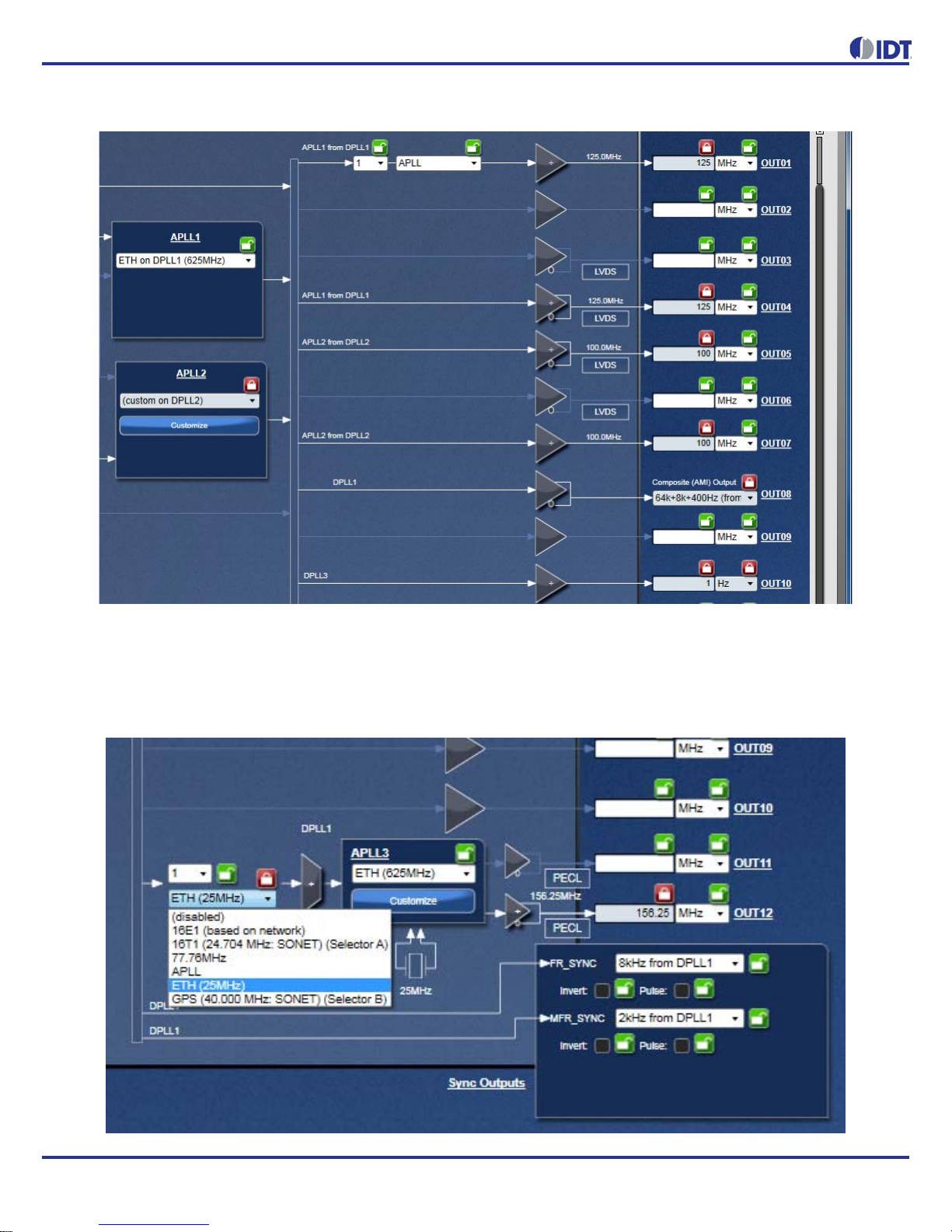
7. Output Configuration. Most output frequencies can be entered for OUT01~OUT12 and they will be automatically
configured. However, 19.2MHz and 10MHz-based clocks are not supported by the default hardware profiles for the
APLLs. Therefore, APLL1/APLL2 needs to be pre-configured to the applicable VCO frequency.
◦To configure APLL1, select “(custom on DPLL1)” as shown in Figure 12.
Figure 12. APLL1 Parameters for VCO = 614.4MHz
Click on the “Customize” button and ignore the initial Timing Commander error. Enter the values as shown in Figure 13
below to get a VCO of 614.4MHz.

REVISION C 09/29/14 13
82P33731/33831EVALUATIONBOARD
Figure 13. APLL1 Parameters for VCO = 614.4MHz
◦To configure APLL2, select “(custom on DPLL1)” as shown in Figure 12. Then click on “Customize” button and ignore
the initial Timing Commander error. Enter the values as shown in Figure 14 below.
Figure 14. Configure APLL2 Parameters for VCO = 600.0MHz
◦Once APLL1 and APLL2 have been configured, output frequencies can now be entered at OUT01 ~ OUT04 (APLL1),
OUT05~OUT07(APLL2) and OUT08~OUT10 (DPLLs).
14 REVISION C 09/29/14
82P33731/33831 EVALUATION BOARD
Figure 15. Output Frequencies Entered after APLL1/APLL2 Configured (example)
◦To configure APLL3, select the correct clock path and enter desired output frequencies in OUT11 and/or OUT12. Only
OUT11 and OUT12 are from APLL3. Please see portion of the window configuring APLL3 in Figure 16 below. Writing
to APLL3-related registers requires an additional step. Refer to Step 8 (Figure 19 and Figure 20) below for details.
Figure 16. Configure APLL3 by selecting a proper clock path and enter desired frequencies in OUT11 and
OUT12
REVISION C 09/29/14 15
82P33731/33831EVALUATIONBOARD
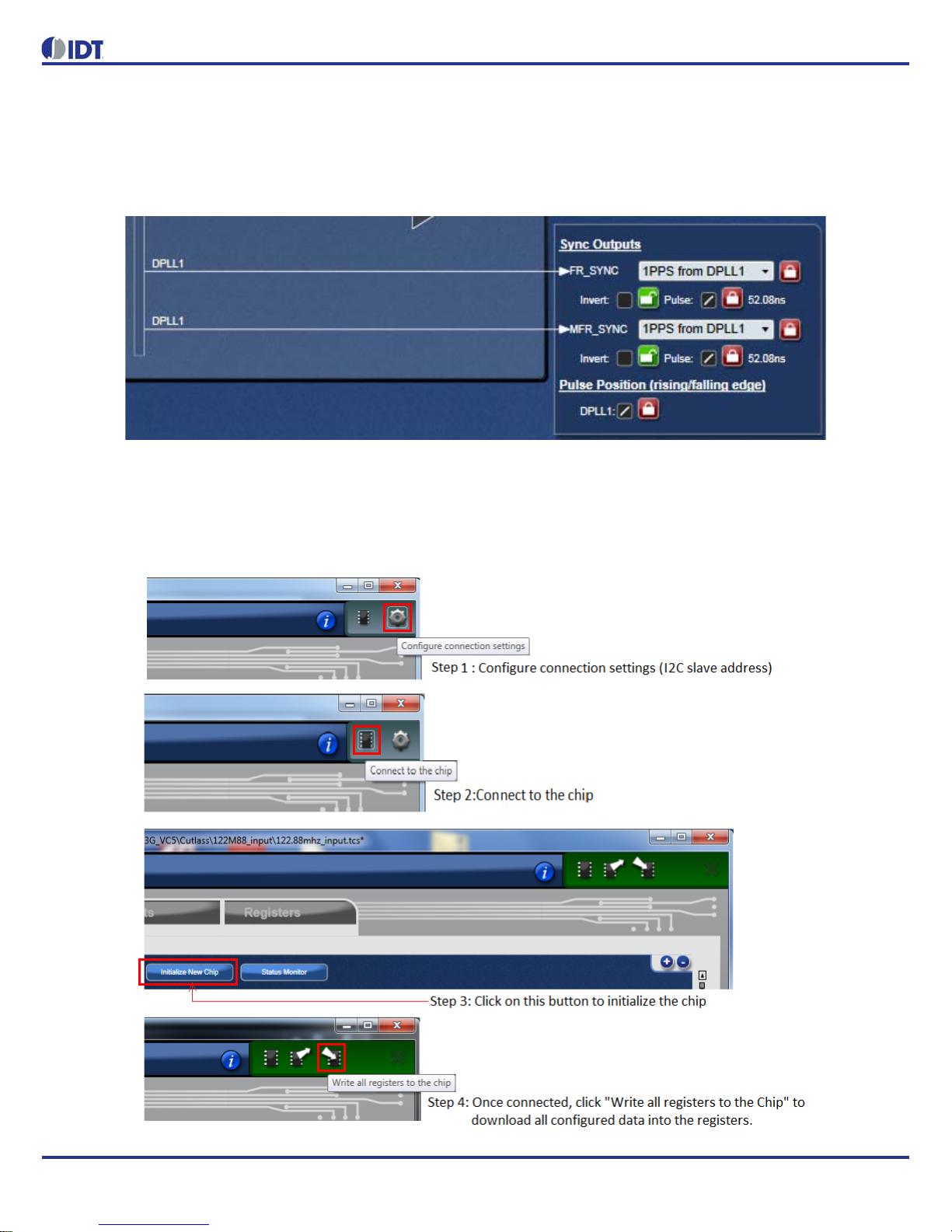
◦Finally, FRSYNC & MRFRSYNC can be configured, if needed. Change FRSYNC & MFRSYNC to 1PPS. By default,
the duty cycle of sync outputs is 50/50. If a pulse is desired, click on the applicable check box. The pulse width is
based on OUT01 clock period.
Figure 17. Configure MRSYNC and MRFRSYNC
8. Connecting to the Board. GUI Configurations can be made before making the USB/I2C connection to the board.
Alternatively, USB connection to the board can be established before TimingComander GUI configuration. It's
recommendedto completeinitial configurationsbeforemaking a USB/I2C connection to the board and write registers into
the device registers. Please follow the steps below in Figure 18 to make a connection to the board.
Figure 18. Steps to Making Connections and Writing to the Board
16 REVISION C 09/29/14
82P33731/33831 EVALUATION BOARD
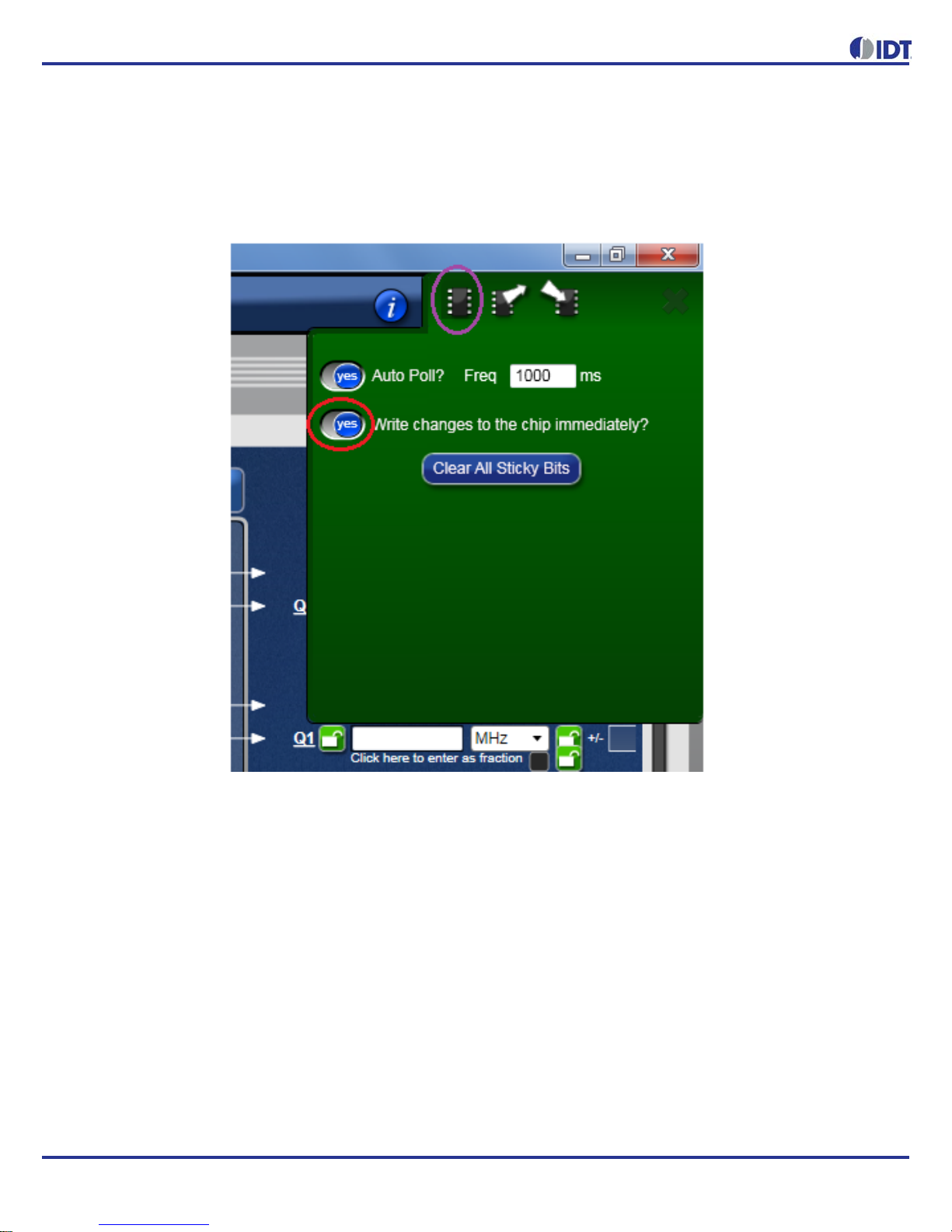
Before making a USB/I2C connection to the board, all configurations discussed in Step 1~8 above are stored in GUI until
the board is connected and configuration data are written to the device. Once the board is connected, by default, any
changes to the GUI configurations will be instantaneously written to the respective registers unless this feature is turned
off. See Figure 19 below to turn on or off “Write changes to the chip immediately”.
Figure 19. By default, any modifications to the existing configuration data will be written to the device
registers immediately
If the feature is turned off, changes in configurations will be written to the chip by clicking on “Writing all registers to the
chip” button.
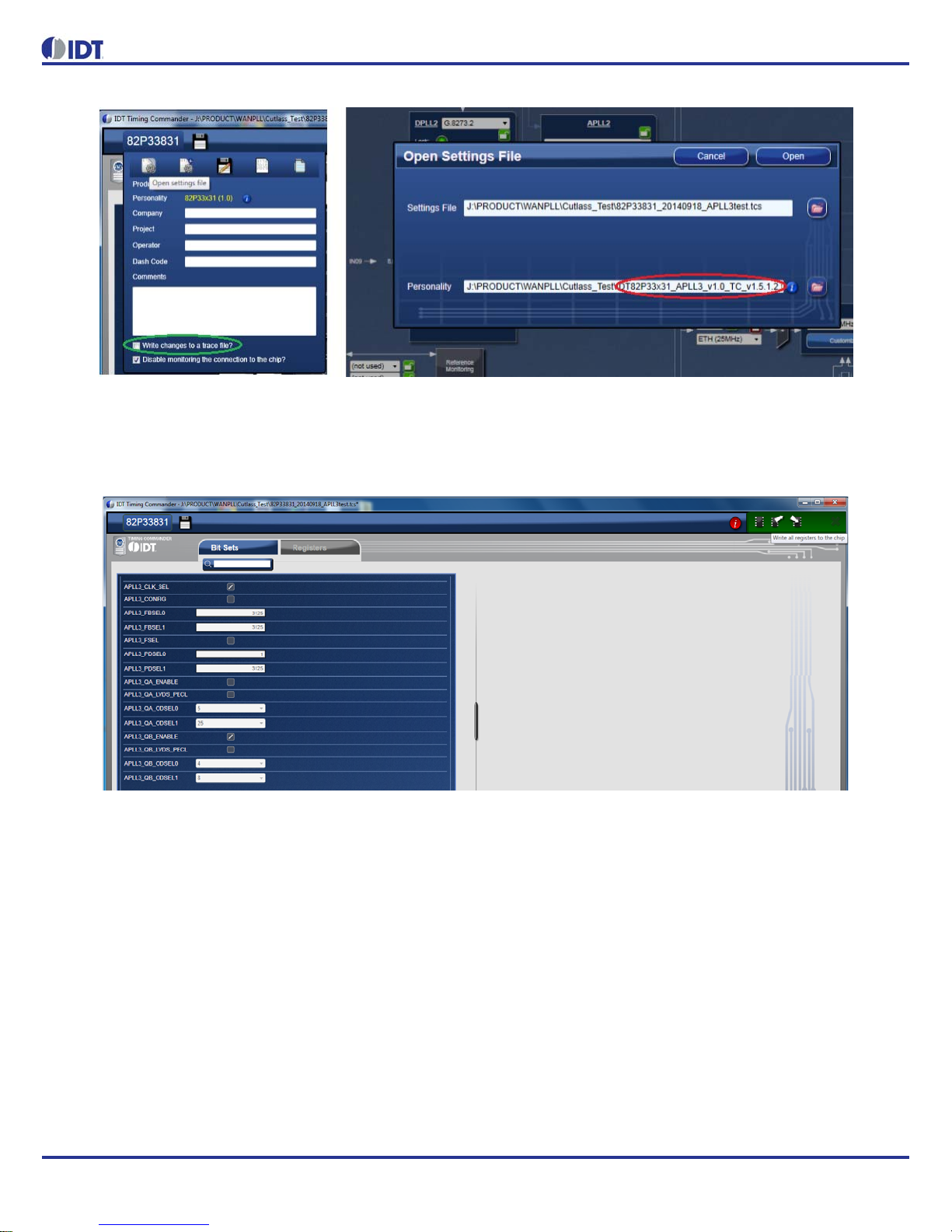
9. Writing to APLL3 related-registers. The step described above will connect to the device and write to all registers
EXCEPT APLL3-related registers. In order to write APLL3 registers, take the following steps:
◦Click on the top, left corner where device part number is displayed. Click on the first symbol (“Opening Setting File” is
shown when the mouse hovers on it). A window to open Personality File and Setting File pops out. See Figure 20
below. Note: (1) un-check “Write to a trace file” box (green oval in the figure below); (2) use the same setting file
where all frequencies are configured (including APLL3); for Personality file, use the file that is solely for APLL3 (see
red oval in the following figure).
REVISION C 09/29/14 17
82P33731/33831EVALUATIONBOARD
Figure 20. Opening Setting File and Personality File for Writing APLL3-related Register
◦Once the same setting file and APLL-only personality file are selected, click on Open, a window for writing APLL3 will
open, as shown below in Figure 21. Following the same procedure as shown in Figure 18 to connect and write to
APLL3.
Figure 21. Connect to the Board and Write to APLL3-related Registers
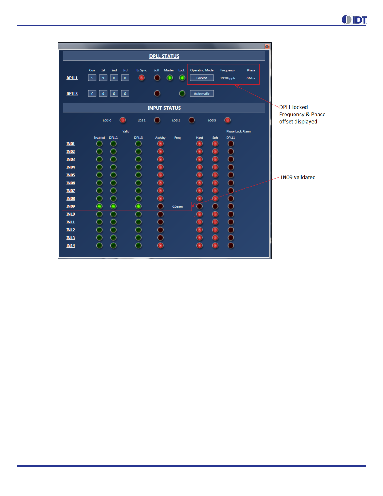
10.Viewing Status – After writing all registers, with configured input reference clocks available, the PLL is supposed to lock
to the reference clock. The PLL operation status can be updated and viewed by clicking “View Status” button in GUI
window. The status window looks like the following (Figure 22). Enabled input reference clock will show with a lit LED.
Frequency offset will also be shown. Locking status of the DPLL will be indicated as “Locked” or otherwise as “Free-run”
or “Holdover”. The frequency and phase offset of the output clock with respect to the input reference will be indicated.
18 REVISION C 09/29/14
82P33731/33831 EVALUATION BOARD
Figure 22. DPLL Status Window

REVISION C 09/29/14 19
82P33731/33831EVALUATIONBOARD
Board Schematics
Figure 23. 82P33x31 Evaluation Board Schematics - Page 1: Block Diagram

20 REVISION C 09/29/14
82P33731/33831 EVALUATION BOARD
Figure 24. 82P33x31 Evaluation Board Schematics - Page 2: Reference Selection
This manual suits for next models
1
Table of contents
Other IDT Motherboard manuals

IDT
IDT ZWIR4532 User manual

IDT
IDT Tsi340-RDK1 User manual

IDT
IDT VersaClock 3S User manual

IDT
IDT 89EB-LOGAN-19 User manual

IDT
IDT 5P49V5907 Manual

IDT
IDT 9FGV1005 Operating instructions

IDT
IDT VersaClock 5 User manual

IDT
IDT 89EBPES16T4G2 User manual

IDT
IDT P9241-G-EVK User manual

IDT
IDT P9242-R-EVK User manual

IDT
IDT EVK-UFT285-6-7 User manual

IDT
IDT Tsi382 LQFP User manual

IDT
IDT 8A 72QFN Series User manual

IDT
IDT ADC1410S Series User manual

IDT
IDT ZMOD4410 User manual

IDT
IDT ZNRG2061 User manual

IDT
IDT 9ZXL1951D User manual

IDT
IDT 89EBPES16NT2 User manual

IDT
IDT VersaClock 3S User manual

IDT
IDT PhiClock 9FGV1001 User manual


