IDT 9FGV1005 Operating instructions

1©2018 Integrated Device Technology, Inc. March 7, 2018
Register Descriptions
The register descriptions section describes the behavior and function of the customer-programmable non-volatile-memory registers in the
9FGV1005 clock generator.
For details of product operation, refer to the product datasheet.
9FGV1005 Clock Register Set
The device contains volatile (RAM) 8-bit registers and non-volatile 8-bit registers (Figure 1). The non-volatile registers are One-Time
Programmable (OTP) and will be pre-programmed at the factory with a custom dash-code configuration.
The device operates according to settings in the RAM registers. At power-up a pre-programmed configuration is transferred from OTP to
RAM registers. The device behavior can then be modified by reprogramming the RAM registers through I2C.
The device can start up in “I2C mode” or in “Hardware Select Mode”, depending upon the status of the REF0_SEL_I2C# pin at power up.
Also see the datasheet. I2C access is only possible when the device has started up in I2C mode. Startup in I2C mode is default when no
pull-up is added to the REF0_SEL_I2C# pin. Pre-programming settings determine which of the 4 OTP banks is loaded into RAM registers
at power up in I2C mode. Using I2C commands, the configuration can be changed and there are also commands to reload a configuration
from a different OTP bank.
Figure 1. Register Maps
User Configuration Table Selection
At power-up, the voltage at OUT0_SEL_I2CB pin 24 is latched by the part and used to select the state of SEL0/SCL and SEL1/SDA pins
(Table 1).
When a weak pull-up (10kΩ) is placed on REF0_SEL_I2C#, the SEL0/SCL and SEL1/SDA pins will be configured as hardware select
inputs, SEL0 and SEL1. Connecting SEL0 and SEL1 to VDDD and/or GND selects one of 4 configuration register sets, CFG0 through
CFG3, which is then loaded into the non-volatile configuration registers to configure the clock synthesizer. The CFG0 through CFG3
configurations are preprogrammed at the factory according to customer specifications and assigned a specific (dash) part number.
When a weak pull-down is placed on REF0_SEL_I2C# (or when it is left floating to use internal pull-down), the pins SEL0 and SEL1 will
be configured as an I2C interface's SDA and SCL slave bus. Configuration register set CFG0 is commonly loaded into the non-volatile
configuration registers to configure the clock synthesizer but the device can be configured to load any of the other configurations. The
host system can use the I2C bus to update the volatile RAM registers to change the configuration, and to read status registers.
9FGV1005 Register Descriptions and
Programming Guide
2©2018 Integrated Device Technology, Inc. March 7, 2018
9FGV1005 Register Descriptions and Programming Guide
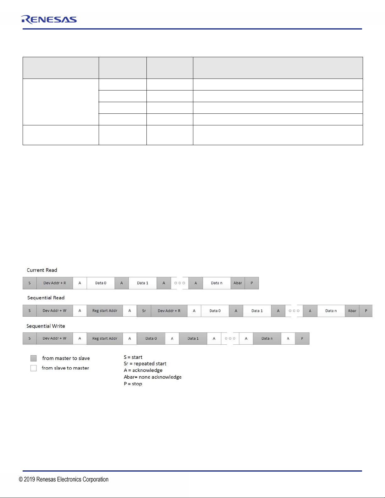
I2C Interface and Register Access
When powered up in I2C mode, the device allows access to internal RAM registers. The default device address is 0xD0 for 8 bits or 0x68
for 7 bits. The device can be preprogrammed for addresses in the range 0xD0-D2-D4-D6 for 8 bits or 0x68-69-6A-6B for 7 bits. The
device acts as a slave device on the I2C bus using one of the four I2C addresses to allow multiple devices to be used in the system. The
interface accepts byte-oriented block write and block read operations. Two address bytes specify the register address of the byte position
of the first register to write or read. Data bytes (registers) are accessed in sequential order from the lowest to the highest byte (most
significant bit first). Read and write block transfers can be stopped after any complete byte transfer. During a write operation, data will not
be moved into the registers until the STOP signal is received, at which point, all data received in the block write will be written
simultaneously in the registers.
For full electrical I2C compliance, it is recommended to use external pull-up resistors for SDATA and SCLK. The internal pull-up resistors
have a size of 100kΩtypical.
Figure 2. I2C R/W Sequence
Table 1. Power-Up Setting of Hardware Select Pin vs I2C Mode, and Default OTP Configuration Register
OUT0_SEL_I2CB Strap at
Power-Up SEL1/SDA pin SEL0/SCL pin Function
10kΩpull-up
0 0 OTP bank CFG0 used to initialize RAM configuration registers.
0 1 OTP bank CFG1 used to initialize RAM configuration registers.
1 0 OTP bank CFG2 used to initialize RAM configuration registers.
1 1 OTP bank CFG3 used to initialize RAM configuration registers.
10kΩpull-down or floating SDA SCL I2Cbus enabled to access registers.
OTP bank CFG0 used to initialize RAM configuration registers.
3©2018 Integrated Device Technology, Inc. March 7, 2018
9FGV1005 Register Descriptions and Programming Guide
Table 2. RAM Overview
Register Address Function Description
0x00 Device / I2C settings.
0x01 REF output settings.
0x02
Reserved.0x03
0x04
0x05
OUT1 output settings.0x06
0x07
0x08
Reserved.0x09
0x0A
0x0B
OUT0 output settings.0x0C
0x0D
0x0E Crystal oscillator settings.
0x0F
0x10
Reserved.
0x11
0x12
0x13
0x14
0x15
0x16
0x17
0x18
0x19
0x1A PLL miscellaneous.
0x1B
0x1C
PLL loop filter settings.0x1D
0x1E
0x1F PLL feedback divider value.
4©2018 Integrated Device Technology, Inc. March 7, 2018
9FGV1005 Register Descriptions and Programming Guide
See Table 3 for details at the bit level.
0x20
Integer output divider values.0x21
0x22
0x23 Reserved.
0x24 Reserved.
0x25 Miscellaneous device settings.
Table 3. RAM Register Map
Register Address Register Bit Default Function Description
Decimal Hex
00 0x00
7 0 Device preprogrammed? 0 = No, 1 = Yes.
[6..5] 00 I2C device address. 00 = 0xD0 / 0x68, 01 = 0xD2 / 0x69, 10 = 0xD4 / 0x6A,
11= 0xD6 / 0x6B 1.
[4..2] 00 Reserved.
[1..0] 00 Load configuration number at power-up 2.
01 0x01
[7..6] 01 Enable REF outputs: 0x = REF0 disabled (unused), 10 = REF0 enabled.
50Reserved.
4 0 Behavior when REF is unused: 0 = Logic “0”, 1 = High impedance (tri-state).
[3..2] 11 REF outputs power supply voltage: 00 = 01 = 1.8V, 10 = 2.5V, 11 = 3.3V.
[1..0] 11 Reserved.
02 0x02 [7..0] 03-hex Reserved.
03 0x03 [7..0] 34-hex Reserved.
04 0x04 [7..0] 54-hex Reserved.
05 0x05
7 1 Enable OUT1: 0 = Disabled (unused), 1 = Enabled.
[6..4] 000
OUT1 configuration:
000 = LP-HCSL, Low-power HCSL.
001 = CMOS1, Single-ended CMOS on true output pin.
011 = LVDS.
100 = CMOS2, Single-ended CMOS on complementary output pin.
101 = CMOSD, Differential CMOS.
111 = CMOSP, Two single-ended CMOS outputs, in-phase.
010 and 110 are not used.
[3..2] 00 OUT1 power supply voltage: 00 = 01 = 1.8V, 10 = 2.5V, 11 = 3.3V.
[1..0] 11 Reserved.
Table 2. RAM Overview
Register Address Function Description
5©2018 Integrated Device Technology, Inc. March 7, 2018
9FGV1005 Register Descriptions and Programming Guide
06 0x06
70Reserved.
6 0 Behavior when OUT1 is unused: 0 = Logic “0”, 1 = High impedance (tri-state).
5 1 OUT1 LP-HCSL slew rate control: 0 = Slow, 1 = Fast.
4 1 OUT1 LP-HCSL impedance control: 0 = 85Ωdifferential, 1 = 100Ωdifferential.
[3..0] 0100 OUT1 LP-HCSL amplitude control: 650mVpp at 0000 – 950mVpp at 1111.
07 0x07
70Reserved.
[6..4] 101 OUT1 LVDS common mode control: 8μA at 000 – 11.5μA at 111.
30Reserved.
[2..0] 100 OUT1 LVDS amplitude control: 30μA at 000 – 65μA at 111.
08 0x08 [7..0] 03-hex Reserved.
09 0x09 [7..0] 34-hex Reserved.
10 0x0A [7..0] 54-hex Reserved.
11 0x0B
7 1 Enable OUT0: 0 = Disabled (unused), 1 = Enabled.
[6..4] 000
OUT0 configuration:
000 = LP-HCSL, Low-power HCSL.
001 = CMOS1, Single-ended CMOS on true output pin.
011 = LVDS.
100 = CMOS2, Single-ended CMOS on complementary output pin.
101 = CMOSD, Differential CMOS.
111 = CMOSP, Two single-ended CMOS outputs, in-phase.
010 and 110 are not used.
[3..2] 00 OUT0 power supply voltage: 00 = 01 = 1.8V, 10 = 2.5V, 11 = 3.3V.
[1..0] 11 Reserved.
12 0x0C
70Reserved.
6 0 Behavior when OUT0 is unused: 0 = Logic “0”, 1 = High impedance (tri-state).
5 1 OUT0 LP-HCSL slew rate control: 0 = Slow, 1 = Fast.
4 1 OUT0 LP-HCSL impedance control: 0 = 85Ωdifferential, 1 = 100Ωdifferential.
[3..0] 0100 OUT0 LP-HCSL amplitude control: 650mVpp at 0000 – 950mVpp at 1111.
13 0x0D
70Reserved.
[6..4] 101 OUT0 LVDS common mode control: 8μA at 000 – 11.5μA at 111.
30Reserved.
[2..0] 100 OUT0 LVDS amplitude control: 30μA at 000 – 65μA at 111.
Table 3. RAM Register Map (Cont.)
Register Address Register Bit Default Function Description
Decimal Hex

6©2018 Integrated Device Technology, Inc. March 7, 2018
9FGV1005 Register Descriptions and Programming Guide
14 0x0E
7 1 Crystal oscillator LDO: 0 = Disabled, 1 = Enabled.
60Reserved.
[5..0] 000000
Crystal oscillator X1 pin capacitance: Cap (pF) = 7.98 + 0.442 × Bits[5..0].
See section Crystal Load Capacitance Registers for crystal oscillator load
capacitance configuration.
15 0x0F
7 1 Crystal oscillator circuit: 0 = Disabled, 1 = Enabled.
60Reserved.
[5..0] 000000 Crystal oscillator X2 pin capacitance: Cap (pF) = 7.98 + 0.442 × Bits[5..0].
16 0x10 [7..0] 83-hex Reserved.
17 0x11 [7..0] 1A-hex Reserved.
18 0x12 [7..0] 0C-hex Reserved.
19 0x13 [7..0] 80-hex Reserved.
20 0x14 [7..0] 00-hex Reserved.
21 0x15 [7..0] 02-hex Reserved.
22 0x16 [7..0] 96-hex Reserved.
23 0x17 [7..0] 00-hex Reserved.
24 0x18 [7..0] 00-hex Reserved.
25 0x19 [7..0] 00-hex Reserved.
26 0x1A
71
PLL, VCO band calibration start. Toggle to 0 and back to 1 to trigger a
calibration.
The calibration engages at the moment the bit moves from 0 to 1. The
calibration finds the optimum VCO band for the current VCO frequency.
60
Override VCO band: 0 = use calibrated VCO band, 1 = use VCO band value
in bits [5..0].
[5..0] 100000 VCO band value. See bit 6.
27 0x1B
7 1 Enable VCO: 0 = VCO disabled, 1 = VCO enabled.
6 1 Enable charge pump: 0 = CP disabled, 1 = CP enabled.
5 1 Enable PLL bias: 0 = PLL bias disabled, 1 = PLL bias enabled.
41Bypass3
rd pole in loop filter: 0 = Use 3rd pole, 1 = 3rd pole bypassed.
[3..0] 1100 Reserved.
28 0x1C [7..4] 1010 Loop filter R-zero value.
[3..0] 1111 Reserved.
29 0x1D [7..0] 00-hex Reserved.
Table 3. RAM Register Map (Cont.)
Register Address Register Bit Default Function Description
Decimal Hex
7©2018 Integrated Device Technology, Inc. March 7, 2018
9FGV1005 Register Descriptions and Programming Guide
1To be able to read this info, you already need to know the device address.
2These two bits show the configuration number 0–3 that will be loaded from OTP into registers at power up. When changing these bits
through I2C you instruct the chip to load another configuration from OTP. This is useful for switching between OTP configurations when in
I2C mode. This method is also used to step through each configuration for reading back OTP contents.
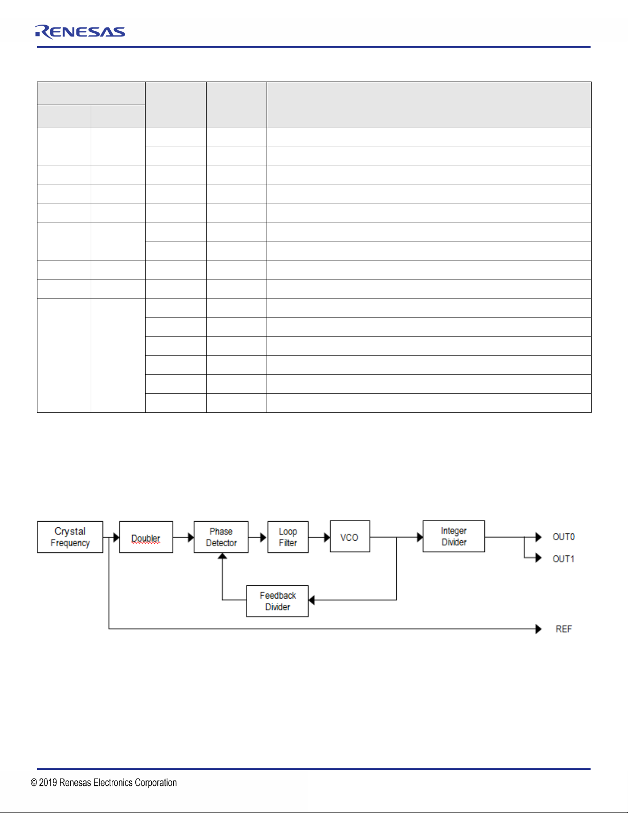
Block Diagram
Figure 3. 9FGV1005 Block Diagram
Equations:
FVCO = FCRYSTAL × Feedback Divider (see register 0x1F).
FOUT0 = FOUT1 = FVCO / Integer Divider (see registers 0x21 and 0x22).
Limits:
FCRYSTAL: 10MHz–40MHz
FVCO: 2300MHz–2600MHz
Integer Output Divider: 8–4095
Feedback Divider: 12–255
30 0x1E [7..4] 0000 Reserved.
[3..0] 1010 Charge pump current, 0 to 750μA with step of 50μA.
31 0x1F [7..0] 24-hex PLL feedback divider value.
32 0x20 [7..0] 12-hex Reserved.
33 0x21 [7..0] 18-hex Integer output divider value, bits [7..0].
34 0x22 [7..4] 0000 Integer output divider value, bits [11..8].
[3..0] 0000 Reserved.
35 0x23 [7..0] 00-hex Reserved.
36 0x24 [7..0] 21-hex Reserved.
37 0x25
70Reserved.
6 1 Enable Integer output divide: 0 = disabled, 1 = enabled.
5 1 Enable crystal frequency doubler: 0 = disabled, 1 = enabled.
[4..3] 00 Reserved.
2 1 Integer output divide enable: 0 = disabled, 1 = enabled.
[1..0] 01 Reserved.
Table 3. RAM Register Map (Cont.)
Register Address Register Bit Default Function Description
Decimal Hex
8©2018 Integrated Device Technology, Inc. March 7, 2018
9FGV1005 Register Descriptions and Programming Guide
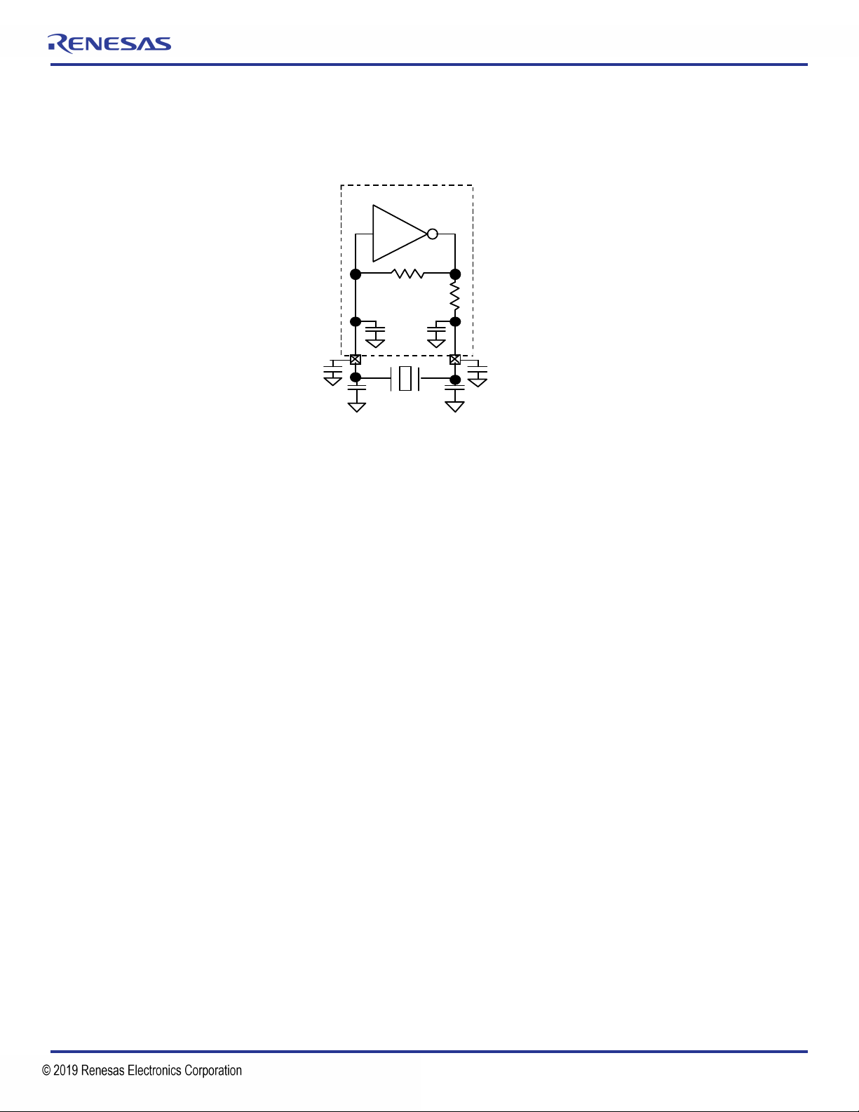
Crystal Load Capacitance Registers
Registers 0x0E and 0x0F contain Crystal X1 and X2 Load capacitor settings that are used to add load capacitance to X1 and X2 (also
known as XIN and XOUT) respectively.
Figure 4. Crystal Oscillator Circuit
Ci1 and Ci2 are on-chip capacitors that are programmable.
Cs is stray capacitance in the PCB and Ce is external capacitors for frequency fine tuning or for achieving load capacitance values
beyond the range of the on-chip programmability. Consult the factory when adding Ce capacitors. The oscillator gain reduces with added
capacitance and there may be crystal oscillator startup issues when adding too much capacitance.
All these capacitors combined make the load capacitance for the crystal.
Capacitance on pin XIN or X1: Cx1 = Ci1 + Cs1 + Ce1.
Capacitance on pin XOUT or X2: Cx2 = Ci2 + Cs2 + Ce2.
Total Crystal Load Capacitance CL= Cx1 × Cx2 / (Cx1+Cx2).
For optimum balance and oscillator gain it is recommended to design Cx1 = Cx2. In that case CL= Cx1 / 2 = Cx2 / 2.
The capacitance per pin X1 or X2 is: Cap (pF) = 7.98 + 0.442 × Bits[5..0].
This includes an estimated Cs1 = Cs2 = 1.0pF.
When designing Cx1 = Cx2, the formula for CL is: CL(pF) = 3.99 + 0.221 × Bits[5..0].
The minimum CLvalue at Cx1 = Cx2 = '00 0000'-binary = 3.99pF.
The maximum CLvalue at Cx1 = Cx2 = '10 1111'-binary = 3.99 + 0.221 × 47 = 14.38pF
Example: For a crystal CLof 8pF, the registers can be programmed as follows:
CL(pF) = 3.99 + 0.221 × 18 = 7.97pF (nearest to 8.0pF).
So for CL= 8pF, the recommended settings are Cx1[5..0] = Cx2[5..0] = 18 or '01 0010'-binary.
Registers 0x0E = 0x0F = 92-hex (= '1001 0010' binary).
.
R
F
GM
R
S
X
2
X1
Xtal Oscillator
Cs1
C i1
Cs
2
C i
2
Ce
1
Ce
2

9©2018 Integrated Device Technology, Inc. March 7, 2018
DISCLAIMER Integrated Device Technology, Inc. (IDT) and its affiliated companies (herein referred to as “IDT”) reserve the right to modify the products and/or specifications described herein at any time,
without notice, at IDT’s sole discretion. Performance specifications and operating parameters of the described products are determined in an independent state and are not guaranteed to perform the same
way when installed in customer products. The information contained herein is provided without representation or warranty of any kind, whether express or implied, including, but not limited to, the suitability
of IDT's products for any particular purpose, an implied warranty of merchantability, or non-infringement of the intellectual property rights of others. This document is presented only as a guide and does not
convey any license under intellectual property rights of IDT or any third parties.
IDT's products are not intended for use in applications involving extreme environmental conditions or in life support systems or similar devices where the failure or malfunction of an IDT product can be rea-
sonably expected to significantly affect the health or safety of users. Anyone using an IDT product in such a manner does so at their own risk, absent an express, written agreement by IDT.
Integrated Device Technology, IDT and the IDT logo are trademarks or registered trademarks of IDT and its subsidiaries in the United States and other countries. Other trademarks used herein are the property
of IDT or their respective third party owners. For datasheet type definitions and a glossary of common terms, visit www.idt.com/go/glossary. Integrated Device Technology, Inc.. All rights reserved.
Tech Support
www.IDT.com/go/support
Sales
1-800-345-7015 or 408-284-8200
Fax: 408-284-2775
www.IDT.com/go/sales
Corporate Headquarters
6024 Silver Creek Valley Road
San Jose, CA 95138 USA
www.IDT.com
9FGV1005 Register Descriptions and Programming Guide
Revision History
Revision Date Description of Change
March 7, 2018 ▪Updated RAM Overview table.
▪Updated RAM Register Map table (addresses 14, 15, 30, and 34).
▪Updated Crystal Load Capacitance formulas.
October 11, 2017 Initial release.

Corporate Headquarters
TOYOSU FORESIA, 3-2-24 Toyosu,
Koto-ku, Tokyo 135-0061, Japan
www.renesas.com
Contact Information
For further information on a product, technology, the most
up-to-date version of a document, or your nearest sales
office, please visit:
www.renesas.com/contact/
Trademarks
Renesas and the Renesas logo are trademarks of Renesas
Electronics Corporation. All trademarks and registered
trademarks are the property of their respective owners.
IMPORTANT NOTICE AND DISCLAIMER
RENESAS ELECTRONICS CORPORATION AND ITS SUBSIDIARIES (“RENESAS”) PROVIDES TECHNICAL
SPECIFICATIONS AND RELIABILITY DATA (INCLUDING DATASHEETS), DESIGN RESOURCES (INCLUDING
REFERENCE DESIGNS), APPLICATION OR OTHER DESIGN ADVICE, WEB TOOLS, SAFETY INFORMATION, AND
OTHER RESOURCES “AS IS” AND WITH ALL FAULTS, AND DISCLAIMS ALL WARRANTIES, EXPRESS OR IMPLIED,
INCLUDING, WITHOUT LIMITATION, ANY IMPLIED WARRANTIES OF MERCHANTABILITY, FITNESS FOR A
PARTICULAR PURPOSE, OR NON-INFRINGEMENT OF THIRD PARTY INTELLECTUAL PROPERTY RIGHTS.
These resources are intended for developers skilled in the art designing with Renesas products. You are solely responsible
for (1) selecting the appropriate products for your application, (2) designing, validating, and testing your application, and (3)
ensuring your application meets applicable standards, and any other safety, security, or other requirements. These
resources are subject to change without notice. Renesas grants you permission to use these resources only for
development of an application that uses Renesas products. Other reproduction or use of these resources is strictly
prohibited. No license is granted to any other Renesas intellectual property or to any third party intellectual property.
Renesas disclaims responsibility for, and you will fully indemnify Renesas and its representatives against, any claims,
damages, costs, losses, or liabilities arising out of your use of these resources. Renesas' products are provided only subject
to Renesas' Terms and Conditions of Sale or other applicable terms agreed to in writing. No use of any Renesas resources
expands or otherwise alters any applicable warranties or warranty disclaimers for these products.
(Rev.1.0 Mar 2020)
© 2020 Renesas Electronics Corporation. All rights reserved.
Table of contents
Other IDT Motherboard manuals

IDT
IDT 8A 72QFN Series User manual

IDT
IDT Tsi340-RDK1 User manual

IDT
IDT ZWIR4532 User manual

IDT
IDT PhiClock 9FGV1001 User manual

IDT
IDT ZMOD4410 User manual

IDT
IDT ZMOD4510-EVK User manual

IDT
IDT EVK-UFT285-6-7 User manual

IDT
IDT VersaClock 6E 5P49V6965 User manual

IDT
IDT P9221-R-EVK User manual

IDT
IDT 82V3911 User manual

IDT
IDT VersaClock 3S User manual

IDT
IDT VersaClock 3S User manual

IDT
IDT ADC1410S Series User manual

IDT
IDT P9241-G-EVK User manual

IDT
IDT P9221-R-EVK User manual

IDT
IDT Tsi620 User manual

IDT
IDT ZSSC41 Series User manual

IDT
IDT ZMID520 Series User manual

IDT
IDT P9242-R-EVK User manual

IDT
IDT 89EBPES24T3G2 User manual


 user guide")


