IDT Tsi84 User manual

®
6024 Silver Creek Valley Road, San Jose, California 95138
Telephone: (800) 345-7015 • (408) 284-8200 • FAX: (408) 284-2775
Printed in U.S.A.
©2009 Integrated Device Technology, Inc.
Tsi384™
Evaluation Board User Manual
60E1000_MA001_08
September 2009

GENERAL DISCLAIMER
Integrated Device Technology, Inc. reserves the right to make changes to its products or specifications at any time, without notice, in order to improve design or performance
and to supply the best possible product. IDT does not assume any responsibility for use of any circuitry described other than the circuitryembodied in an IDT product. The
Company makes no representations that circuitry described herein is free from patent infringement or other rights of third parties which may result from its use. No license is
granted by implication or otherwise under any patent, patent rights or other rights, of Integrated Device Technology, Inc.
CODE DISCLAIMER
Code examples providedby IDT arefor illustrative purposes only and should notbe relieduponfor developing applications.Any use ofthe code examplesbelow is completely
at your own risk. IDT MAKES NOREPRESENTATIONSOR WARRANTIES OFANY KIND CONCERNING THE NONINFRINGEMENT,QUALITY, SAFETY OR SUITABILITY
OF THE CODE, EITHER EXPRESS OR IMPLIED, INCLUDING WITHOUT LIMITATION ANY IMPLIED WARRANTIES OF MERCHANTABILITY, FITNESS FOR A PARTICU-
LAR PURPOSE, ORNON-INFRINGEMENT. FURTHER,IDT MAKES NO REPRESENTATIONS ORWARRANTIES AS TOTHE TRUTH,ACCURACYOR COMPLETENESS
OF ANY STATEMENTS, INFORMATION OR MATERIALS CONCERNING CODE EXAMPLES CONTAINED IN ANY IDT PUBLICATION OR PUBLIC DISCLOSURE OR
THAT IS CONTAINED ON ANY IDT INTERNET SITE. IN NO EVENT WILL IDT BELIABLE FOR ANY DIRECT, CONSEQUENTIAL, INCIDENTAL, INDIRECT, PUNITIVE OR
SPECIAL DAMAGES, HOWEVER THEY MAY ARISE, AND EVEN IF IDT HAS BEEN PREVIOUSLY ADVISED ABOUT THE POSSIBILITY OF SUCH DAMAGES. The code
examples also may be subject to UnitedStates export control lawsand maybe subject to theexportorimportlawsof other countries andit is your responsibility to comply with
any applicable laws or regulations.
LIFE SUPPORT POLICY
Integrated Device Technology's products are not authorized for use as critical components in lifesupport devices or systemsunless a specific written agreement pertaining to
such intended use is executed between the manufacturer and an officer of IDT.
1. Life support devices or systems are devices or systems which (a) are intended for surgical implant into the body or (b) support or sustain life and whose failure to perform,
when properly used in accordance with instructions for use provided in the labeling, can be reasonably expected to result in a significant injury to the user.
2. A critical component is anycomponents of a life supportdevice or system whosefailure to performcanbe reasonably expected tocause the failure of thelife support device
or system, or to affect its safety or effectiveness.
IDT, the IDT logo, and Integrated Device Technology are trademarks or registered trademarks of Integrated Device Technology, Inc.

Tsi384 Evaluation Board User Manual
60E1000_MA001_08
Integrated Device Technology
www.idt.com
3
Contents
About this Document. . . . . . . . . . . . . . . . . . . . . . . . . . . . . . . . . . . . . . . . . . . . . . . . . . . . . 5
Related Information . . . . . . . . . . . . . . . . . . . . . . . . . . . . . . . . . . . . . . . . . . . . . . . . . . . . . . . . . . . . . . . . . . . . . . . . . . . . . . 5
Acronyms . . . . . . . . . . . . . . . . . . . . . . . . . . . . . . . . . . . . . . . . . . . . . . . . . . . . . . . . . . . . . . . . . . . . . . . . . . . . . . . . . . . . . . 5
Revision History . . . . . . . . . . . . . . . . . . . . . . . . . . . . . . . . . . . . . . . . . . . . . . . . . . . . . . . . . . . . . . . . . . . . . . . . . . . . . . . . . 5
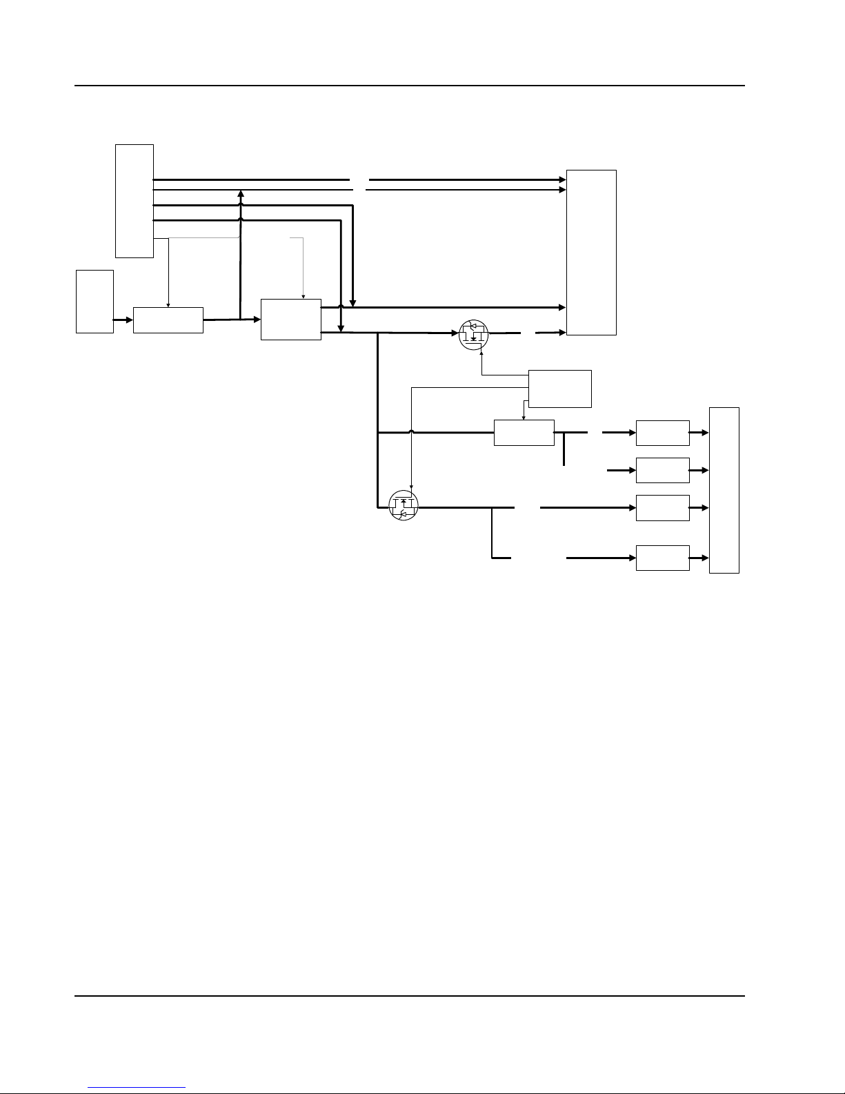
1. Board Design . . . . . . . . . . . . . . . . . . . . . . . . . . . . . . . . . . . . . . . . . . . . . . . . . . . . . . . 9
1.1 Overview . . . . . . . . . . . . . . . . . . . . . . . . . . . . . . . . . . . . . . . . . . . . . . . . . . . . . . . . . . . . . . . . . . . . . . . . . . . . . . . . . 9
1.2 PCI/X Interface . . . . . . . . . . . . . . . . . . . . . . . . . . . . . . . . . . . . . . . . . . . . . . . . . . . . . . . . . . . . . . . . . . . . . . . . . . . 10
1.2.1 Overview . . . . . . . . . . . . . . . . . . . . . . . . . . . . . . . . . . . . . . . . . . . . . . . . . . . . . . . . . . . . . . . . . . . . . . . . 10
1.2.2 IDSEL Signals . . . . . . . . . . . . . . . . . . . . . . . . . . . . . . . . . . . . . . . . . . . . . . . . . . . . . . . . . . . . . . . . . . . . 11
1.2.3 Interrupt Signals. . . . . . . . . . . . . . . . . . . . . . . . . . . . . . . . . . . . . . . . . . . . . . . . . . . . . . . . . . . . . . . . . . . 11
1.2.4 PCI Pull-up Signals . . . . . . . . . . . . . . . . . . . . . . . . . . . . . . . . . . . . . . . . . . . . . . . . . . . . . . . . . . . . . . . . 12
1.2.5 Arbitration . . . . . . . . . . . . . . . . . . . . . . . . . . . . . . . . . . . . . . . . . . . . . . . . . . . . . . . . . . . . . . . . . . . . . . . 12
1.3 PCIe Interface. . . . . . . . . . . . . . . . . . . . . . . . . . . . . . . . . . . . . . . . . . . . . . . . . . . . . . . . . . . . . . . . . . . . . . . . . . . . . 12
1.4 Power Management . . . . . . . . . . . . . . . . . . . . . . . . . . . . . . . . . . . . . . . . . . . . . . . . . . . . . . . . . . . . . . . . . . . . . . . . 13
1.4.1 Power Regulation. . . . . . . . . . . . . . . . . . . . . . . . . . . . . . . . . . . . . . . . . . . . . . . . . . . . . . . . . . . . . . . . . . 13
1.4.2 Power Requirements . . . . . . . . . . . . . . . . . . . . . . . . . . . . . . . . . . . . . . . . . . . . . . . . . . . . . . . . . . . . . . . 13
1.4.3 Power Sequencing . . . . . . . . . . . . . . . . . . . . . . . . . . . . . . . . . . . . . . . . . . . . . . . . . . . . . . . . . . . . . . . . . 15
1.4.4 System Power Design . . . . . . . . . . . . . . . . . . . . . . . . . . . . . . . . . . . . . . . . . . . . . . . . . . . . . . . . . . . . . . 15
1.5 Clock Management . . . . . . . . . . . . . . . . . . . . . . . . . . . . . . . . . . . . . . . . . . . . . . . . . . . . . . . . . . . . . . . . . . . . . . . . 16
1.5.1 PCI/X . . . . . . . . . . . . . . . . . . . . . . . . . . . . . . . . . . . . . . . . . . . . . . . . . . . . . . . . . . . . . . . . . . . . . . . . . . . 16
1.5.2 System Clock Distribution. . . . . . . . . . . . . . . . . . . . . . . . . . . . . . . . . . . . . . . . . . . . . . . . . . . . . . . . . . . 17
1.6 Other Interfaces . . . . . . . . . . . . . . . . . . . . . . . . . . . . . . . . . . . . . . . . . . . . . . . . . . . . . . . . . . . . . . . . . . . . . . . . . . . 18
1.6.1 JTAG Interface. . . . . . . . . . . . . . . . . . . . . . . . . . . . . . . . . . . . . . . . . . . . . . . . . . . . . . . . . . . . . . . . . . . . 18
1.6.2 EEPROM Interface . . . . . . . . . . . . . . . . . . . . . . . . . . . . . . . . . . . . . . . . . . . . . . . . . . . . . . . . . . . . . . . . 18
1.7 Hardware Reset . . . . . . . . . . . . . . . . . . . . . . . . . . . . . . . . . . . . . . . . . . . . . . . . . . . . . . . . . . . . . . . . . . . . . . . . . . . 18
1.8 Logic Analyzer Connectivity. . . . . . . . . . . . . . . . . . . . . . . . . . . . . . . . . . . . . . . . . . . . . . . . . . . . . . . . . . . . . . . . . 18
2. Configurable Options. . . . . . . . . . . . . . . . . . . . . . . . . . . . . . . . . . . . . . . . . . . . . . . . 19
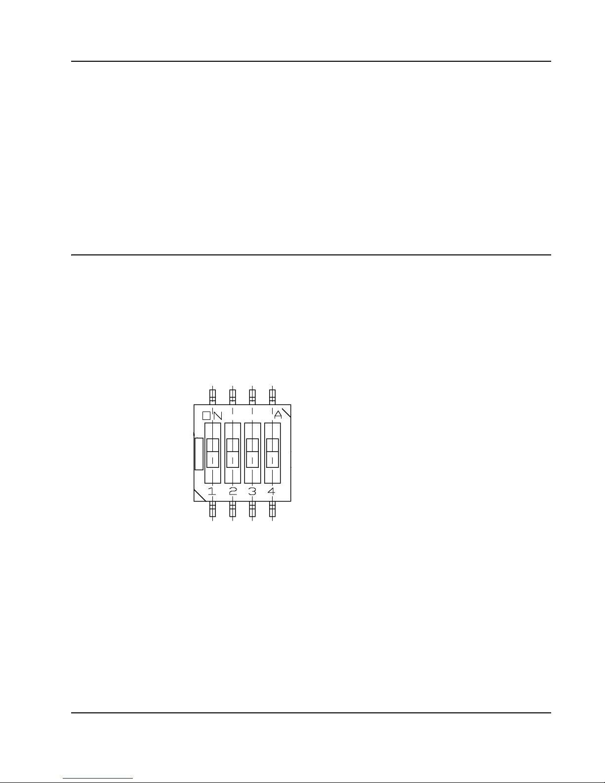
2.1 Switches . . . . . . . . . . . . . . . . . . . . . . . . . . . . . . . . . . . . . . . . . . . . . . . . . . . . . . . . . . . . . . . . . . . . . . . . . . . . . . . . . 19
2.1.1 DIP Switches . . . . . . . . . . . . . . . . . . . . . . . . . . . . . . . . . . . . . . . . . . . . . . . . . . . . . . . . . . . . . . . . . . . . . 19
2.1.2 Push Button . . . . . . . . . . . . . . . . . . . . . . . . . . . . . . . . . . . . . . . . . . . . . . . . . . . . . . . . . . . . . . . . . . . . . . 25
2.2 Shunt Jumpers . . . . . . . . . . . . . . . . . . . . . . . . . . . . . . . . . . . . . . . . . . . . . . . . . . . . . . . . . . . . . . . . . . . . . . . . . . . . 26
2.2.1 J1 Shunt Jumper. . . . . . . . . . . . . . . . . . . . . . . . . . . . . . . . . . . . . . . . . . . . . . . . . . . . . . . . . . . . . . . . . . . 27
2.2.2 J6 Shunt Jumper. . . . . . . . . . . . . . . . . . . . . . . . . . . . . . . . . . . . . . . . . . . . . . . . . . . . . . . . . . . . . . . . . . . 27
2.2.3 J21 Shunt Jumper. . . . . . . . . . . . . . . . . . . . . . . . . . . . . . . . . . . . . . . . . . . . . . . . . . . . . . . . . . . . . . . . . . 27
2.3 Debug Headers. . . . . . . . . . . . . . . . . . . . . . . . . . . . . . . . . . . . . . . . . . . . . . . . . . . . . . . . . . . . . . . . . . . . . . . . . . . . 28
2.3.1 J22 Tsi384 JTAG . . . . . . . . . . . . . . . . . . . . . . . . . . . . . . . . . . . . . . . . . . . . . . . . . . . . . . . . . . . . . . . . . . 29
2.3.2 J23 Logic Analyzer PADs . . . . . . . . . . . . . . . . . . . . . . . . . . . . . . . . . . . . . . . . . . . . . . . . . . . . . . . . . . . 30
2.3.3 J38 CPLD JTAG. . . . . . . . . . . . . . . . . . . . . . . . . . . . . . . . . . . . . . . . . . . . . . . . . . . . . . . . . . . . . . . . . . . 31
2.4 Connectors . . . . . . . . . . . . . . . . . . . . . . . . . . . . . . . . . . . . . . . . . . . . . . . . . . . . . . . . . . . . . . . . . . . . . . . . . . . . . . . 32
2.4.1 J2-J36-J37 Connectors . . . . . . . . . . . . . . . . . . . . . . . . . . . . . . . . . . . . . . . . . . . . . . . . . . . . . . . . . . . . . . 32

Contents4
Tsi384 Evaluation Board User Manual
60E1000_MA001_08 Integrated Device Technology
www.idt.com
2.4.2 J3 ATX Power Connector . . . . . . . . . . . . . . . . . . . . . . . . . . . . . . . . . . . . . . . . . . . . . . . . . . . . . . . . . . . 33
2.4.3 P1 x4 PCIe Finger Connector . . . . . . . . . . . . . . . . . . . . . . . . . . . . . . . . . . . . . . . . . . . . . . . . . . . . . . . . 33
2.5 LEDs . . . . . . . . . . . . . . . . . . . . . . . . . . . . . . . . . . . . . . . . . . . . . . . . . . . . . . . . . . . . . . . . . . . . . . . . . . . . . . . . . . . 34
3. Bill of Materials . . . . . . . . . . . . . . . . . . . . . . . . . . . . . . . . . . . . . . . . . . . . . . . . . . . . .37

5
Tsi384 Evaluation Board User Manual
60E1000_MA001_08
Integrated Device Technology
www.idt.com
About this Document
This document describes how to test the key features of the Tsi384 using the Tsi384 evaluation board.
It can be used in conjunction with the Tsi384 Evaluation Board Schematics.
Related Information
• Tsi384 User Manual
• Tsi384 Evaluation Board Schematics
•PCI Express Base Specification (Revision 1.1)
• PCI Express CEM Specification (Revision 1.1)
•PCI Express-to-PCI/PCI-X Bridge Specification (Revision 1.0)
•PCI-X Addendum to PCI Local Bus Specification (Revision 1.0a)
Acronyms
Revision History
60E1000_MA001_08, Formal, September 2009
This document was rebranded as IDT. It does not include any technical changes.
60E1000_MA001_07, Formal, May 2008
The following changes were made to this version:
• Completed various changes in response to the Tsi384 evaluation board’s removal of support for an
external arbiter (see “Arbitration”).
• Updated the document to support Revision 1.0, Assembly number E1000_AS001_05 of the Tsi384
evaluation board. This assembly version includes the hardware changes listed in the following
table.
Term Definition
PCIe PCI Express
PCI/X PCI or PCI-X bus mode
SerDes Serial/De-serializer

About this Document6
Tsi384 Evaluation Board User Manual
60E1000_MA001_08 Integrated Device Technology
www.idt.com
60E1000_MA001_06, Formal, January 2008
Corrected the descriptions of the S7 and S8 switches. Previously, these descriptions were reversed.
60E1000_MA001_05, Formal, October 2007
Added PCI pull-up resistor values to Table 3.
60E1000_MA001_04, Formal, May 2007
This document supports the Revision 1.0, Assembly number E1000_AS001_03 version of the Tsi384
evaluation board. This assembly version includes the hardware changes listed in the following table.
60E1000_MA001_03, Formal, April 2007
This is the general release version of the document. There are no technical differences between this
document and the previous version.
Evaluation Board Changes – Assembly E1000_AS001_03
Item Previous Usage/Definition New Usage/Definition
U11/Tsi384 Bridge Tsi384-133CLVZ Tsi384-133ILVZ2
PCI_LOCKn pull-up None Add 4.7K +/-1K size 0603 resistor
between pin B39 (LOCK#) and pin B41
(3.3V) on J2
3.3Vaux on J2 No connection Short pin A14 (3.3Vaux) to pin A21
(3.3V) by wiring
3.3Vaux on J36 and J37 No connection Short pin A14 (3.3Vaux) to pin A21
(3.3V) by wiring
JTAG signals pull-up 2K pull-up on R288, R293, R294,
R295 Change to 10K instead
PCI reset C231 was 1uF (0603)
(0603ZD105KAT2A) Changed to 10uF (0603)
MFR P/N: ECJ-1VB0J106M
Evaluation Board Changes – Assembly E1000_AS001_03
Reference Designator Description
Removals
R13 Removed
Reworks
Add 10 K Ohm pull-down to PCI_RST#

About this Document 7
Tsi384 Evaluation Board User Manual
60E1000_MA001_08
Integrated Device Technology
www.idt.com
60E1000_MA001_02, Formal, March 2007
This document includes “Bill of Materials” for the Tsi384 evaluation board. It supports the
Revision 1.0, Assembly number E1000_AS001_02 version of the Tsi384 evaluation board. This
assembly version includes the hardware changes listed in the following table.
60E1000_MA001_01, Formal, March 2007
This is the first version of the Tsi384 Evaluation Board User Manual. This document supports the
Revision 1.0, Assembly number E1000_AS001_01 version of the Tsi384 evaluation board.
Evaluation Board Changes – Assembly E1000_AS001_02
Reference Designator Description
Changes
R88 Change to .015ohm
R242,R272,R6 Change to 1Kohm
C182,C183,C193,
C189,C207,C202 Change to 2.2uF
R148 Populate
R150 Populate
C77,C45 Install
C235 Change to 300nF
R208 130 Ohm
R215 220 Ohm
R220 441 Ohm
R139 2260 Ohm
R144 220 Ohm
R196 441 Ohm
Removals
R141 Remove
Reworks
Add 1kohm resistor pull-up to LOCK#

About this Document8
Tsi384 Evaluation Board User Manual
60E1000_MA001_08 Integrated Device Technology
www.idt.com

9
Tsi384 Evaluation Board User Manual
60E1000_MA001_08
Integrated Device Technology
www.idt.com
1. Board Design
Topics discussed include the following:
•“Overview” on page 9
•“PCI/X Interface” on page 10
•“PCIe Interface” on page 12
•“Power Management” on page 13
•“Clock Management” on page 16
•“Other Interfaces” on page 18
•“Hardware Reset” on page 18
•“Logic Analyzer Connectivity” on page 18
1.1 Overview
The key features of the Tsi384 evaluation board include the following:
• Single x4 lane, 2.5 Gbps PCIe 1.1 compatible riser card (extended height form factor)
• Three PCI/X slots
• 32-/64-bit PCI/X bus, 25–133 MHz operation
• PCI/X power support through system or external supply
• PCIe compliance/debugging test points

1. Board Design10
Tsi384 Evaluation Board User Manual
60E1000_MA001_08 Integrated Device Technology
www.idt.com
Figure 1: Evaluation Board Block Diagram
1.2 PCI/X Interface
1.2.1 Overview
The PCI/X Interface is implemented on the board with three slots, in which one is an R/A mounted
connector on the top of the board. All PCI/X connectors are compliant with the PCI/X 2.0b
specification. Appropriate clearance is provided such that up to three PCI/X cards can be inserted for
testing while the board is in an open-chassis standard ATX case.
EEPROM
TSI384
3.3V PCI/X 64bit 133Mhz Edge Connector
R/A Mount Slot 0 (Top)
PCI/X
Power
Management
PCI Express Card Edge X4
PCIe
LA Probe
JTAG
Header
ATX
Connectors
EEPROM
3.3V PCI/X 64bit 133Mhz Edge Connector
Slot 1 (Middle)
PCI/X Isolation Buffer
3.3V PCI/X 64bit 133Mhz Edge Connector
Slot 2 (Lower)
Clock
Management
PCI/X bus
arbiter

1. Board Design 11
Tsi384 Evaluation Board User Manual
60E1000_MA001_08
Integrated Device Technology
www.idt.com
The PCI/X Interface supports the configurations listed in Table 1.
The support for PCI-X 133 MHz operation is possible with the use of an isolation buffer. The R/A
connector located on the top of board is available in this maximum frequency. The PCI bus is routed
forward and returned to the other slots to expand the bus for multi-slot support.
1.2.2 IDSEL Signals
IDSEL signals are connected in the following order:
• Slot 0 – R/A connector top slot: 2K ohms to AD16 (Device 0)
• Slot 1 – Vertical middle slot: 2K ohms to AD19 (Device 3)
• Slot 2 – Vertical lower slot: 2K ohms to AD18 (Device 2)
The 2K ohm resistor value is consistent with the ability of the Tsi384 to drive the AD lines 2 clock
cycles prior in PCI mode, and 4 clock cycles prior in PCI-X mode. The PCI/X Interface is unterminated
with the exception of the clock signals.
1.2.3 Interrupt Signals
The PCI interrupt signals are connected to the slots as shown in Table 2.
Table 1: PCI/X Interface — Supported Configurations
Protocol Operating
Speed (MHz) Number of Slots
Supported
PCI 25, 33, 50, 66 3
PCI-X 50, 66 3
PCI-X 100 2
PCI-X 133 1
Table 2: PCI Interrupt Routing
Tsi384 Slot 0 Slot 1 Slot 2
AADC
BBAD
CCBA
DDCB

1. Board Design12
Tsi384 Evaluation Board User Manual
60E1000_MA001_08 Integrated Device Technology
www.idt.com
1.2.4 PCI Pull-up Signals
The following signals have a pull-up resistor on the PCI bus.
1.2.5 Arbitration
The Tsi384 evaluation board has provisions to implement an external arbiter; however, the current PCB
assembly does not have the external arbiter implemented. Therefore, the only valid mode of operation
is internal arbiter enabled.
1.3 PCIe Interface
The Tsi384 evaluation board implements a four-line PCIe interface. It is designed to connect onto a
PCIe system with a standard x4 finger connector. The system must provide the REFCLK and PERSTN
signals. The PCIe interface has the following design elements:
• Supports Hot insertion and removal
• Mid-bus logic analyzer pads for PCIe RXD/TXD signal probing
• AC coupling on the TXD lanes
• JTAG TDI - TDO loopback for chain continuity
Table 3: PCI Pull-up Signals
Signal Description Resistor Value
PCI_CBE#[4:7] Byte enables for upper 32-bit AD lines 8.2K
PCI_REQ#[0:3] Bus request 8.2K
PCI_GNT#[0:3] Bus grant 8.2K
PCI_FRAME# Control signal 8.2K
PCI_IRDY#, PCI_TRDY# Control signal 8.2K
PCI_STOP# Control signal 8.2K
PCI_SERR# System error 8.2K
PCI_PERR# Parity error 8.2K
PCI_PAR Parity of lower 32-bit lines and CBE bus 8.2K
PCI_PAR64 Parity of upper 32-bit AD lines and CBE bus 8.2K
PCI_DEVSEL# Device select line 8.2K
PCI_INT#[A:D] Interrupt line 2.4K
PCI_PME# PCI Power Management Event occurred 8.2K

1. Board Design 13
Tsi384 Evaluation Board User Manual
60E1000_MA001_08
Integrated Device Technology
www.idt.com
1.4 Power Management
1.4.1 Power Regulation
The evaluation board’s power regulation is implemented as follows:
• Digital 3.3V power supply available from DC/DC regulator or ATX supply
• Digital 1.2V switching regulator
• PCIe supplies filtered using EMI ferrite networks
To support PCI/X cards, the following additional power resources are included:
• 12V to 5V DC/DC converter
• 12V to 3.3V DC/DC converter
• External power connectors – ATX 20-pin connector for supplying all power from an ATX power
supply
1.4.2 Power Requirements
The power requirements and implementation for the Tsi384 is as follows.
The target power draw of the Tsi384 is a maximum of 2 Watts, all supplies combined. The supplies to
the Tsi384 are controlled during ramp up using enable pins on regulators and switches.
1.4.2.1 PCIe
The PCIe CEM Specification 1.1 defines power limits on PCIe slots according to the number of lanes
available on the card. Power rules regarding x4 PCIe slots are a maximum of 25W slot. Current limits
are included in Table 5.
Table 4: Tsi384 Power Requirements
Supply Name Symbol Supplied Source
Device Core 1.2V_384 DC/DC switching regulator w/Enable pin
PCIe 1.2V Core 1.2V_A_384 Passive Filter
PCI 3.3v supply 3.3V_384 Power switch w optional Ferrite filter to reduce
EMI/noise from PCI environment
PCIe 3.3v supply 3.3V_A_384 Passive Filter
Table 5: PCIe Connector Current Limits
Rail Current
3.3V 3A
12V 2.1A

1. Board Design14
Tsi384 Evaluation Board User Manual
60E1000_MA001_08 Integrated Device Technology
www.idt.com
In both cases (x4 or x16), the usage of the 12V supply provides access to the full 25W/75W available
from the system to the board. The PCIe pinout design includes more 12V power pins as it allows more
power-per-pin capability. The evaluation board regulates all power from the 12V system rail; however,
3.3V from the system remains unused.
1.4.2.2 PCI/X
The PCISIG defines the power rules regarding PCI/X cards as a maximum of 25 Watts per card (All
power rails combined power draw). The individual current limits on voltage rails are included in
Table 6.
It is not possible “within spec” to provide the full power required to the PCI/X without violating the
specification while drawing power from only a x4 PCIe system. Up to 23W not including regulator
efficiency losses can be made available. The evaluation board provides the power requirements in one
of two ways depending on the application:
• PCIe system power
• ATX System connector
The following conditions summarize the power available for a single PCI/X card without external
supply. An efficiency of 85% is taken into account for switching regulators. These limits can be
exceeded in cases where the system can provide more than the suggested limit, which is usually only
implemented in hot swap systems.
Table 6: PCI/X Connector current limits
Rail Current
3.3v 7.6a
5v 5a
-12v 100ma
12v 500ma
Table 7: PCI/X Connector Current Limit with No External Supply
Rail Supplying Topology Current (Maximum)
3.3V 12V to 3.3V regulator 6A
12V 12V directly 500mA
-12V N/A N/A
5V 12V to 5V regulator 4A

1. Board Design 15
Tsi384 Evaluation Board User Manual
60E1000_MA001_08
Integrated Device Technology
www.idt.com
For additional slots, or in cases where the system cannot supply enough power, a separate ATX power
connector is used to power the card. The evaluation board senses the presence of this supply, and
disables the slave PCIe slot power. For the case of a separate external ATX supply, all three slots are
provided with the required power.
1.4.3 Power Sequencing
On power-up, the card power sequencing is as follows:
1. 1.2V powered on
2. PCI/X I/O slot power and pull-ups, and Tsi384 3.3V
12V/-12V/5V PCI are not sequence controlled.
1.4.4 System Power Design
Figure 2 illustrates the power distribution for the riser card. The following list is a functional summary
of the power design:
1. Sequencing control over the following rails:
•3.3VPCI
• 3.3V Tsi384 I/O/PCIe AVDD
• 1.2V Tsi384 Core/PCIe VDD
2. ATX 20-pin connector override, which disables all power draw from the PCIe system
3. Current sensing of Tsi384 supplies

1. Board Design16
Tsi384 Evaluation Board User Manual
60E1000_MA001_08 Integrated Device Technology
www.idt.com
Figure 2: System Power Distribution
1.5 Clock Management
The Tsi384 requires up to two input clocks to operate:
• 25–133MHz clock for PCI/X
• 100-MHz reference clock for PCIe
The PCI/X and PCIe input clocks are briefly discussed.
1.5.1 PCI/X
The evaluation board supports master and slave clocking for PCI/X.
• Master – When in master mode, the Tsi384 generates the required PCI/X clock for all slots.
• Slave – When in slave mode, an on-board selectable 25–133 MHz clock generator is used as
follows:
3v3/5v DC/DC
Regulator
(LM4600)
PCIe
System
12v
ATX
20-pin
-12v
12v
5v
3.3v
Unused
GND
1.2v DC/DC
12V
3.3V
1.2V
Power
Sequencer
3.3v/5v Disable
1.2V PCIE_VDD
3.3V PCIE AVDD
-12V
3.3V I/O
PCI/X
Bus
Connectors
Current
Sense
Current
Sense
Current
Sense
Current
Sense
Tsi384
Electronic/Mech
Breaker w/
Current Limit

1. Board Design 17
Tsi384 Evaluation Board User Manual
60E1000_MA001_08
Integrated Device Technology
www.idt.com
— Low skew distribution buffer to all slots and Tsi384
— External clock input for any optional testing
1.5.1.1 PCIe
For PCIe clocking, a 100-MHz differential HCSL clock source is required. The clock source is
available in two forms:
• Edge connector clock source – This clock source synchronizes the system SerDes with the Tsi384.
• On-board 100-MHz reference – This clock source can separate the clock domains between the
bridge and the root complex.
The two PCIe clock sources are multiplexed with an analog multiplexer to select between the system
clock or on-board clock (see Figure 3).
1.5.2 System Clock Distribution
Figure 3 shows the distribution of the system clock on the Tsi384 evaluation board.
Figure 3: System Clock Distribution
Tip
To multiplex the sources of two clocks, passive resistor muxes are located at the endpoints of
the clock nets. For more information, see the Tsi384 Evaluation Board Schematic
(60E1000_SC002).
ICS87604I
PCIe System
PCIe_REFCLK
PCI/X
Bus
Connectors
Tsi384
PCI_CLK
CLKOUT[0:4] PCI_INT_CLK[0:2,4]
PCI_EXT_CLK[0:3]
Passive Mux
(0r0 RES)
PCI_FBK_CLK
PCI_CLK[0:2]
PLD
ICS557-01
Diff.
SMA
Input
Passive
Mux
(0r0 RES)
ANALOG
MUX
PCIe_SYS_CLK
PCIe_GEN_CLK
PCIe_BERT_CLK
PCIe_REF_CLK
(AC coupled)
Config

1. Board Design18
Tsi384 Evaluation Board User Manual
60E1000_MA001_08 Integrated Device Technology
www.idt.com
1.6 Other Interfaces
1.6.1 JTAG Interface
To support debug and testing of device, JTAG access to the Tsi384 is available using a standard JTAG
header for Wiggler connection.
1.6.2 EEPROM Interface
A single EEPROM device socket is available for programming registers during startup. The socket is
in an 8-pin DIP format.
1.7 Hardware Reset
Figure 4 illustrates the reset options of the Tsi384 evaluation board.
Figure 4: Board Reset
Three levels of reset are available:
• Cold reset – This reset is applied during power up. System (card edge) PCIe_PERSTn is muxed
with the board’s reset controller.
• Warm reset – This reset is activated by a push-button reset on the board.
• Hot reset – This reset is activated by the in-band message sent by the root complex. No supporting
hardware is necessary.
1.8 Logic Analyzer Connectivity
The serial buses have Midbus pads (TMS818 probe) for visibility of SerDes lines using a
pre-processor. Each probing pad provides access to the RX and TX segments of a x4 link.
To access the PCI/X bus, a Nexus PCI/X interposer card can be used with Tektronix mictor cables. The
card can be plugged into any PCI edge slot, or in-line with the device under test.
Tip
For more information on cold, warm, and hot reset levels, see the “Resets, Clocking, and
Initialization Options” chapter in the Tsi384 User Manual.
PCI Express Edge Connector X4
Reset
Controller
SYS_PCIe_PERSTn
PUSHBUTTON PCIe_PERSTn

19
Tsi384 Evaluation Board User Manual
60E1000_MA001_08
Integrated Device Technology
www.idt.com
2. Configurable Options
Topics discussed include the following:
•“Switches” on page 19
•“Shunt Jumpers” on page 26
•“Debug Headers” on page 28
•“Connectors” on page 32
•“LEDs” on page 34
2.1 Switches
2.1.1 DIP Switches
Switches S1 to S6 combine four, small slide switches identified with numbers 1 to 4 (see Table 8 for
individual switch definition).
Figure 5: DIP Switch Package/Individual Switch Position
ON
OFF

2. Configurable Options20
Tsi384 Evaluation Board User Manual
60E1000_MA001_08 Integrated Device Technology
www.idt.com
Figure 6: Switch Locations
SW1
S8
S7
S3
S4
S1 S2
S5
S6
SW2
Table of contents
Other IDT Motherboard manuals

IDT
IDT 89EBPES12N3 User manual

IDT
IDT 9ZXL1951D User manual

IDT
IDT ZMOD4410 User manual

IDT
IDT ADC1410S Series User manual

IDT
IDT Tsi382 LQFP User manual

IDT
IDT EB4T4 Eval Board User manual

IDT
IDT VersaClock 6 5P49V69 Series User manual

IDT
IDT 9FGV1006 User manual

IDT
IDT VersaClock 3S User manual

IDT
IDT P9241-G-EVK User manual

IDT
IDT 8A 72QFN Series User manual

IDT
IDT P9221-R-EVK User manual

IDT
IDT ZMOD4510-EVK User manual

IDT
IDT 8A34xxx 48QFN series User manual

IDT
IDT 89EBPES16T4G2 User manual

IDT
IDT P9242-G-EVK User manual

IDT
IDT 89EBPES16NT2 User manual

IDT
IDT Tsi620 User manual

IDT
IDT EB8T5A Eval Board User manual

IDT
IDT 82P33731 User manual