IDT VersaClock 6E 5P49V6965 User manual
1©2019 Integrated Device Technology, Inc. June 17, 2019
Introduction
The VersaClock®6E programmer board is made to ease the programming of blank 5P49V6965 or 5P49V6975 devices. With the
on-board USB interface, the IDT Timing Commander™ GUI can be used to communicate with the VersaClock®6E device in the socket
for configuration and programming of its OTP memory.
Board Overview
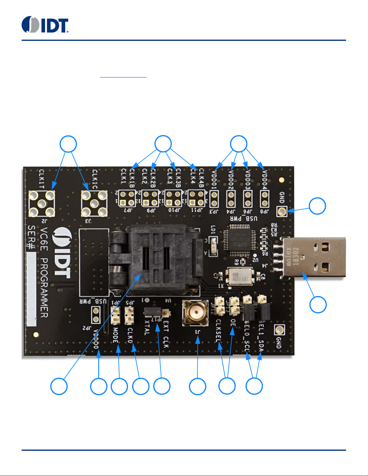
Use Figure 1 and Table 1 to identify board items and features.
Figure 1. Programmer Board Overview
11 12
10
9
13
1
8 7 65432
VersaClock®6E – 5P49V6965 and 5P49V6975
Programmer Board User Guide
2©2019 Integrated Device Technology, Inc. June 17, 2019
VersaClock®6E – 5P49V6965 and 5P49V6975 Programmer Board User Guide
Connecting the Board to a Computer
The programmer board can be plugged into a USB port of a personal computer directly, or, a USB extension cable can be used if that is
more convenient. The on-board USB-to-I2C bridge (FTDI chip) does the data communication and the +5V in the USB bus powers the
on-board regulator. The board can fully function with just the USB connection to a computer.
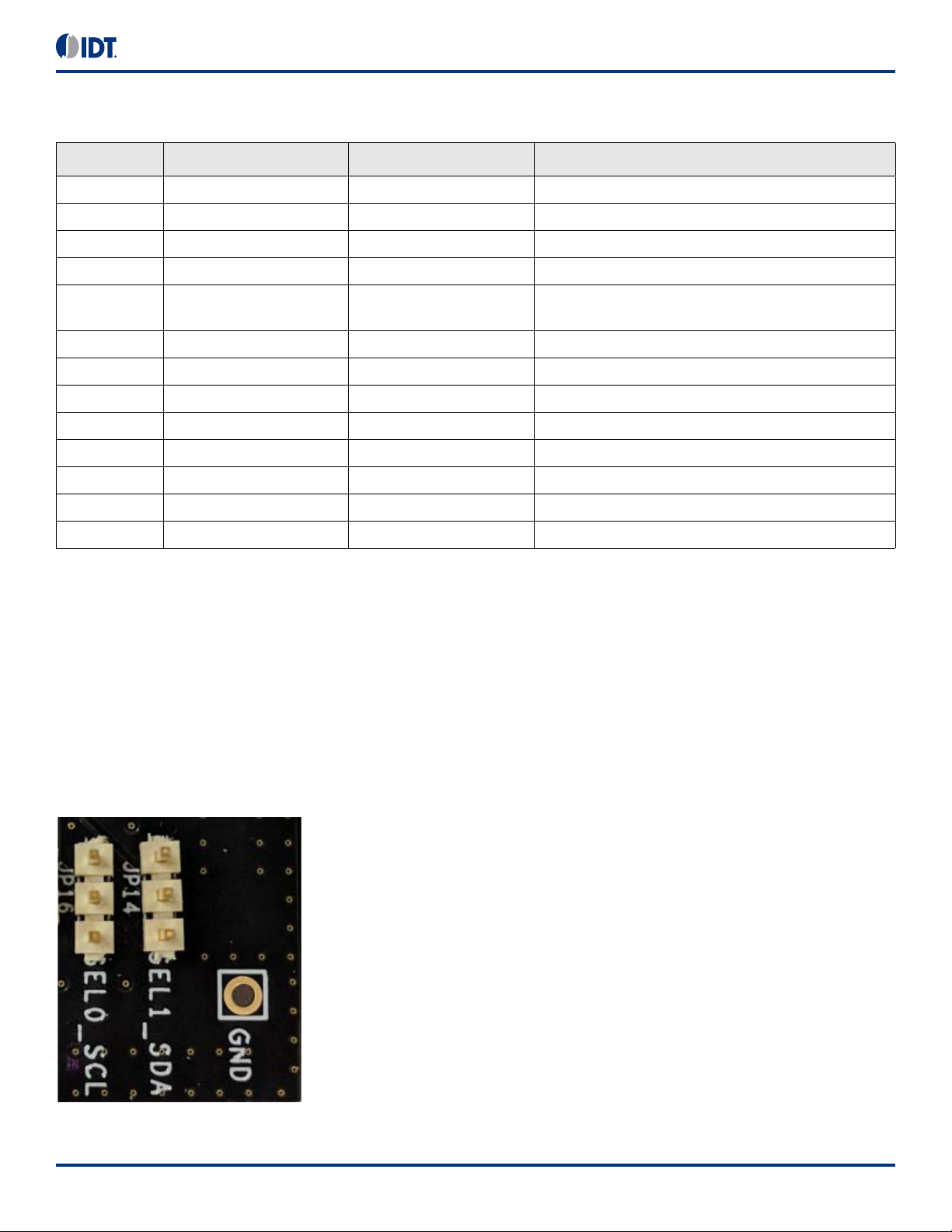
JP 14 and JP16 Functionality
JP14 and JP16 have multiple functions. The center pin of JP14 connects to the SEL1/SDA pin on the 5P49V6965/6975 and the center pin
of JP16 connects to the SEL0/SCL pin on the 5P49V6965/6975.
Figure 2. JP14 and JP16 Jumpers
The bottom pins connect to the FTDI USB-to-I2C bridge. To use Timing Commander to communicate to the chip, jumpers need to be
placed between the center and bottom pins as in Figure 3.
Table 1. 5P49V6965/5P49V6975 Programmer Board Pins and Functions
Label Number Name On-board Connector Label Function
1 USB J4 USB connector.
2 I2C / SEL JP14, JP16 Jumpers to connect I2C or control SEL0/1.
3 OE / CLKSEL JP12, JP13 Jumpers to control OE and CLKSEL.
4 Ref Clock Input J1 SMA to connect alternative Ref Clock.
5 Input Clock Select JP17 Select between on-board 25MHz crystal and alternative
Ref Clock.
6 Output 0 JP5 Differential input clock, Sens output.
7 Operation Mode JP1 Jumper to select I2C or Hardware Select Mode.
8 VDDO0 JP2 Optional VDD for output 0.
9 DUT Socket U4 Socket for 5P49V6965/6975. Pin 1 is lower left.
10 Output 1 Diff J2, J3 Optional output 1 differential connection.
11 Outputs 1, 2, 3, 4 J7, J9, J10, J11 2 × 2 pin probe points for outputs 1, 2, 3 and 4.
12 VDDO1, 2, 3, 4 JP3, JP4, JP6, JP8 Optional VDD for outputs 1, 2, 3 and 4.
13 Ground — Ground reference for general purpose.

3©2019 Integrated Device Technology, Inc. June 17, 2019
VersaClock®6E – 5P49V6965 and 5P49V6975 Programmer Board User Guide
Figure 3. JP14 and JP16 for I2C
Figure 4. JP14 and JP16 for SEL0/1
After programming multiple configurations, the 5P49V6965/6975 can be restarted in Hardware Select mode and then the SEL0 and SEL1
pins can be used to select a configuration. The SEL0/1 pins on the 5P49V6965/6975 have pull-down resistors on the chip so when
leaving the pins open, like Figure 2, both SEL0 and SEL1 are low and configuration 0 is selected. The upper pins in JP14 and JP16 are
pulled up to VDD so when placing jumpers as in Figure 4, the SEL0 and SEL1 pins are pulled up. Placing the jumpers as in Figure 4
selects configuration 3. Also see the chapter about the Mode jumper to use the Hardware Select mode.
JP14 and JP16 also allow wiring of the I2C bus into a system. As mentioned above, the bottom pins connect to the FTDI USB-to-I2C
bridge. For SCL connect to the bottom pin of JP16, for SDA connect to the bottom pin of JP14 and for ground use the GND test point to
the right of JP14 and JP16. These three wires can be connected to a 5P49V6965/6975 that is assembled in a system so Timing
Commander can be used to control this remote 5P49V6965/6975.

4©2019 Integrated Device Technology, Inc. June 17, 2019
VersaClock®6E – 5P49V6965 and 5P49V6975 Programmer Board User Guide
JP12 and JP13 Functionality
JP12 controls the CLKSEL pin and JP13 controls the SD/OE pin on the 5P49V6965/6975. These pins have pull-down resistors on the
chip so when the pins are left open, the pins will be pulled low. When placing a jumper, the pin will be pulled high. This way the
functionality of the CLKSEL and SD/OE pins can be verified.
Figure 5. JP12 and JP13 Jumpers
J1 and JP17 Functionality
The programmer board has a 25MHz crystal assembled for use with the 5P49V6965. This 25MHz crystal is the default and recommended
crystal. To use the 25MHz crystal, place a jumper to the left on JP17, as in Figure 6. In case a different input frequency is needed, the
jumper can be moved to the right, to connect J1 to the crystal input pin on the 5P49V6965. Using an RF generator, a different frequency
can be applied to the crystal input pin through J1. The recommended amplitude is 0dBm to +3dBm or 600mVpp to 1Vpp.
The 5P49V6975 has an integrated crystal and therefore, J1 / JP17 have no function.
Figure 6. SMA and JP17 Jumper

5©2019 Integrated Device Technology, Inc. June 17, 2019
VersaClock®6E – 5P49V6965 and 5P49V6975 Programmer Board User Guide
JP1 and JP5 Functionality
JP5 is the CLK0 output (OUT0) of the 5P49V6965/6975. The upper pin is ground and the lower pin is the actual output. Connect a probe
between the upper (GND) and lower (OUT0) pins to measure the OUT0 frequency or waveform. JP1 can be used to select the operating
Mode to be either I2C Mode or Hardware Select Mode. The mode is selected at power up so at the moment the board is plugged into a
USB port. The proper method for using JP1 is to first unplug the board from USB, then change the JP1 jumper and plug the board back
into a USB port. No jumper on JP1 selects the I2C mode where Timing Commander can communicate with the device. Having a jumper
installed on JP1 selects the Hardware Select Mode for selecting a pre-programmed configuration with the SEL0 and SEL1 jumpers.
Figure 7. JP1 Jumper and JP5 Pins
JP7, JP9, JP10 and JP11 Functionality
These four 2 × 2 test points are connected to the four differential outputs on the 5P49V6965/6975. The lower two pins are ground and the
upper two pins are the actual output pins. A probe can be used to check the outputs, to measure the frequency or to check the waveform
with an oscilloscope. Connect a single ended probe between a ground pin and output pin or connect a differential probe between the two
output pins. Note that the output pins connect directly to the pins on the chip and there are no additional components for termination or
biasing. For HCSL and LVPECL logic types, additional biasing is needed to allow the outputs to make sufficient signal swing.
Figure 8. JP7, JP9, JP10 and JP11 for CLK1, 2, 3 and 4 (OUT1, 2, 3 and 4)

6©2019 Integrated Device Technology, Inc. June 17, 2019
VersaClock®6E – 5P49V6965 and 5P49V6975 Programmer Board User Guide
J2 and J3 Functionality
J2 and J3 are SMA footprints for an alternative differential connection to OUT1. The default programmer board does not have these
connectors assembled.
Figure 9. J2 and J3 Alternative CLK1 (OUT1)
JP3, JP4, JP6 and JP8 Functionality
The default programmer board does not have jumper pins assembled for JP3, JP4, JP6 and JP8. The two pins in each jumper are
shorted on the board with a 0 ohm resistor. The lower pins are connected to a 3.3V power regulator on the board. The upper pins are
each connected to a different VDDO pin. So the programmer board connects each VDDO pin to 3.3V by default. This is sufficient when
programming 5P49V6965 or 5P49V6975 devices and checking output frequencies. Jumper pins can be installed and the 0 ohm resistors
can be removed to gain control of the VDDO pins. A jumper can be placed to connect to the on-board 3.3V regulator. Remove the jumper
and connect the upper pin to an external power supply, in case a different voltage is needed. The ground side of the power supply can be
connected to the GND point on the right.
Figure 10. JP3, JP4, JP6 and JP8 VDDO Connections
VC6E Programmer Board Compatibility
The VC6E programmer board hardware was designed for the 5P49V6965 and 5P49V6975 but is backwards compatible with older VC6
and VC5 devices. Essentially, this VC6E programmer board can do everything and more than the older VC5 programmer board.
This VC6E programmer board can be used with the following devices:
▪Using the VC6E Timing Commander personality: 5P49V6965 and 5P49V6975.
▪Using the VC6 Timing Commander personality: 5P49V6901, 5P49V6913 and 5P49V6914.
▪Using the VC5 Timing Commander personality: 5P49V5901, 5P49V5913, 5P49V5914, 5P49V5923, 5P49V5925, 5P49V5927,
5P49V5929, 5P49V5933 and 5P49V5935.
This VC6E Programmer Board User Guide will only deal with the VC6E Timing Commander personality.
7©2019 Integrated Device Technology, Inc. June 17, 2019
VersaClock®6E – 5P49V6965 and 5P49V6975 Programmer Board User Guide
Configuration and Setup
Use the following steps to setup the 5P49V6965 or 5P49V6975 device using USB-to-I2C and start the configuration.
1. Before connecting the programmer board to USB, make sure JP1 is open (no jumper). Also see JP1 functionality and Figure 7.
2. Connect J4 to the USB port of a PC.
3. Launch VersaClock 6E Timing Commander Software (refer to VersaClock 6E Timing Commander User Guide). Download the
VersaClock 6E Timing Commander User Guide.
4. Following the Getting Started steps in the Timing Commander software, an I2C connection is established between the GUI software
and the VersaClock 6E chip.
5. Select “Open Settings File” if you have existing settings or “New Settings File” and select 5P49V6965 or 5P49V6975 depending on the
device in the socket. In the same screen, browse for the VersaClock 6E personality file, by clicking on the button at the bottom right.
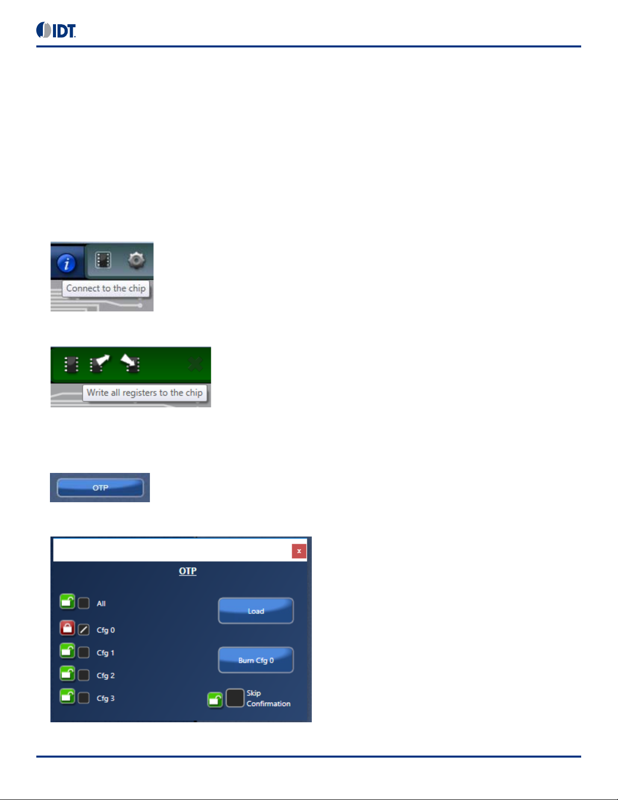
6. Connect to the device by clicking on the microchip icon located at the top right of the Timing Commander screen.
7. Once connected, new options will be available on a green background indicating that Timing Commander has successfully connected
with the device in the socket. Write settings to the chip by clicking on the write all registers to the chip option.
8. All intended outputs should now be available for measurement. At this point only the volatile memory (registers) is programmed. When
unplugging the board to remove power, the configuration is erased.
9. After connecting to the chip, the OTP button will be available to enter the menu for burning OTP. First enter a configuration before
burning OTP. Configurations can be burned only once.
10. After opening the OTP Burn menu, one or more configurations can be selected for burning to OTP. In the example below, only
configuration 0 is selected to be burned to OTP.
8©2019 Integrated Device Technology, Inc. June 17, 2019
VersaClock®6E – 5P49V6965 and 5P49V6975 Programmer Board User Guide
11. After finishing the burning to OTP, the device can be tested as follows:
•Unplug USB to remove power.
•Place JP1 to make the device start in Hardware Select mode the next time USB (power) is plugged in again.
•Place jumpers on JP14 and JP16 for selecting a specific configuration. No jumpers for configuration 0. Also see JP14 and JP16
functionality above. For checking configuration 0, it is not necessary to place a jumper on JP1. When starting in I2C mode,
configuration 0 is loaded by default.
•Plug in USB to power up the board and the correct frequencies should be available on outputs, according to the configuration that
was burned to OTP.
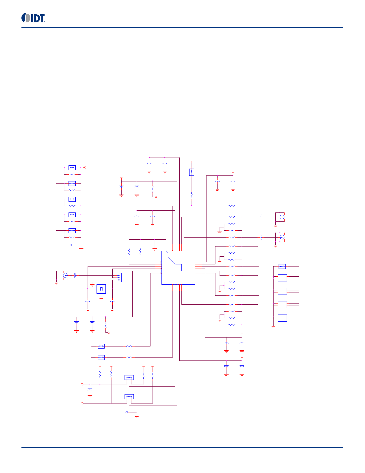
Schematics
Programmer board schematics are shown on the following pages.
Figure 11. 5P49V6965/6975 Programmer Board Schematics – page 1
XTL
CLK1T
TP2
CLK2B
R45 0
1 2
CLKSEL_J
CLK1
C17
1u
12
C29
0. 1u_N P
1 2
VDDO4
OUT2B
VDD D
R42 0
1 2
VDDO2
TP1
JP10
He ader_4Pin
1
3
2
4
CLK0
R35 33
1 2
R31 33
1 2
C27
1u
12
VDDO0
R21 33
1 2
Output
Probe
Connections
C13
0.1u
12
USB_PWR
VDDO1
C16
0.1u
12
R27 33
1 2
R15
10K
1 2
JP9
He ader_4Pin
1
3
2
4
C11
1u
12
JP3
VDDO1_NP
1 2
CLK4
U4
5P49V6965
CLKIN
1
CLKINB
2
XO U T
3
XI N / R E F
4
VDD A
5
CLKSEL
6
SD/OE
7
SEL1/SDA
8
SEL0/SCL
9
VDDO4
10
OUT4
11
OUT4B
12
OUT3B 13
OUT3 14
VDDO3 15
OUT2B 16
OUT2 17
VDDO2 18
OUT1B 19
OUT1 20
VDDO1 21
VDDD 22
VDDO0 23
OUT0_SELB_I2C 24
e_PAD 25
CLK0
R18 220
1 2
CLK1C
JP16
SCL/SEL0
1
2
3
R26 33
1 2
CLKINB
R14
0
12
CLK4B
R30 33
1 2
OUT1B
JP12
CLKSEL
1 2
CLK3
OUT1
R38
4.7k
1 2
C25
1u
12
CLK4
C26
0.1u
12
C23
0.1u
12
SEL0_SC L
VDDO3
VDDD
OUT4B
C20
10p(np)
12
CLK2B
R46 0
1 2
OUT3B
CLK1
VDD D
CLK2
PU
SDOE_J
JP13
OE
1 2
CLK1C
R20 33
1 2
CLK3B
CLK2
R36
1K
12
CLK1B
SDOE
C19
10nF
1 2
JP1
Mode
12
J2
SMA_STRAIGHT_pin_NP
GND
VDDO4
CLK3
MODE
VDDO1
VDDD
R32 220
1 2
I2C
SDA
XI N _ R EF
GND
JP8
VDDO4_NP
1 2
SEL1_SDA
PU
C24
0.1u
12
XIN
R41
10K
1 2
C22
1u
12
R24 220
1 2
X2
25MHz
1 3
2
4
VDDO3
CLKSEL
C28
47pF
12
JP7
He ader_4Pin
1
3
2
4
C18
0.1u
12
R17 33
1 2
R28 220
1 2
OUT2
CLK1B
Optional
External
Power
JP2
VDDO0_NP
1 2
JP4
VDDO2_NP
1 2
VDDD
R40
10K
1 2
R33 220
1 2
OUT0
I2C
SCL
JP14
SDA/SEL1
1
2
3
J1
USB_PWR
R39
4.7k
1 2
J3
SMA_STRAIGHT_pin_NP
REF
VDDD
R34
2.2
12
JP17
Xtal / Clock
1
2
3
REF
JP5
VDDO0
1 2
R23
100
12
VDDD
R16 33
1 2
C15
1u
12
R25 220
1 2
SEL1_SDA_PIN
CLK4B
C30
0. 1u_N P
1 2
R44 0
1 2
R29 220
1 2
C21
10p(np)
12
GND
OUT3
CLKIN
OUT4
CLK1T
C12
0.1u
12
VDDO2
R37
1K
12
R19 220
1 2
XOU T
USB_PWR
CLK3B
VDDO0
C14
1u
12
R43 0
1 2
SEL0_SCL_PIN
R22
100
12
JP6
VDDO3_NP
1 2
VDDA JP11
He ader_4Pin
1
3
2
4

9©2019 Integrated Device Technology, Inc. June 17, 2019
VersaClock®6E – 5P49V6965 and 5P49V6975 Programmer Board User Guide
Figure 12. 5P49V6965/6975 Programmer Board Schematics – page 2
R13 402_1%
1 2
U3
LM317LBD
VIN
1
VOUT_2
2
VOUT_3
3
Adjust
4
NC_8 8
VOUT_7 7
VOUT_6 6
NC_5 5
XTI N
VCC2232_3V
C10
10uF
C3 0.1uF
1 2
R6 1.5K
1 2
R1
680
12
L1
600 ohm 500mA
C2 0.1uF
1 2
USB_5V
USB_PWR
LD1
Green
3V3_USB
C7
33pF
1 2
SEL1_SDA
C5
0.1uF
12
XTO U T
R12 10K
1 2
USB_5V
C4
10uF
1 2
U1
USB_A
VBUS 1
D+ 3
GND 4
D- 2
3V3_USB
SEL0_SCL
R7 10
1 2
C1 10nF
1 2
R2
470
12
R11
243_1%
12
R9
100
1 2
R3
27
12
VCC2232
C8
33pF
12
R5
27
12
R10
10K
12
3V3_USB
X1
ABMM-6.000MHZ-B2-T (5x7mm)
1 3
2
4
XO Y
Connect C7 between crystal pads 1 and 4.
Connect C8 between crystal pads 2 and 3.
Use 1 via to connect to the ground plane.
U2
f t2232_chip
EESK
1
EEDATA
2
VCC 3
RESET#
4
RSTOUT#
5
3V3OUT
6
USBDP
7
USBDM
8
GND
9
SI/WUA 10
GPIOH3 11
GPIOH2 12
GPIOH1 13
VCCIOA 14
GPIOH0 15
GPIOL3 16
GPIOL2 17
GND
18
GPIOL1 19
GPIOL0 20
TMS/ C S 21
TDO/ D I 22
TDI/DO 23
TCK/ SK 24
GND
25
SI/WUB 26
UNUSED11 27
UNUSED10 28
UNUSED9 29
UNUSED8 30
VCCIOB 31
UNUSED7 32
UNUSED6 33
GND
34
UNUSED5 35
UNUSED4 36
UNUSED3 37
UNUSED2 38
UNUSED1 39
UNUSED0 40
PWREN# 41
VCC 42
XTI N
43
XTO U T
44
AGND
45 AVCC 46
TEST
47
EECS
48
C9
0.1uF
12
GND
R4 10
1 2
C6
0.047uF
12
R8 10K
1 2
VCC2232
DISCLAIMER Integrated Device Technology, Inc. (IDT) and its affiliated companies (herein referred to as “IDT”) reserve the right to modify the products and/or specifications described herein at any time,
without notice, at IDT’s sole discretion. Performance specifications and operating parameters of the described products are determined in an independent state and are not guaranteed to perform the same
way when installed in customer products. The information contained herein is provided without representation or warranty of any kind, whether express or implied, including, but not limited to, the suitability
of IDT's products for any particular purpose, an implied warranty of merchantability, or non-infringement of the intellectual property rights of others. This document is presented only as a guide and does not
convey any license under intellectual property rights of IDT or any third parties.
IDT's products are not intended for use in applications involving extreme environmental conditions or in life support systems or similar devices where the failure or malfunction of an IDT product can be rea-
sonably expected to significantly affect the health or safety of users. Anyone using an IDT product in such a manner does so at their own risk, absent an express, written agreement by IDT.
Integrated Device Technology, IDT and the IDT logo are trademarks or registered trademarks of IDT and its subsidiaries in the United States and other countries. Other trademarks used herein are the property
of IDT or their respective third party owners. For datasheet type definitions and a glossary of common terms, visit www.idt.com/go/glossary. Integrated Device Technology, Inc. All rights reserved.
Tech Support
www.IDT.com/go/support
Sales
1-800-345-7015 or 408-284-8200
Fax: 408-284-2775
www.IDT.com/go/sales
Corporate Headquarters
6024 Silver Creek Valley Road
San Jose, CA 95138 USA
www.IDT.com
10©2019 Integrated Device Technology, Inc. June 17, 2019
VersaClock®6E – 5P49V6965 and 5P49V6975 Programmer Board User Guide User Guide
Ordering Information
Revision History
Orderable Part Number Description
5P49V6965-PROG VC6E Programmer Board + 5P49V6965A000 samples
5P49V6975-PROG VC6E Programmer Board + 5P49V6965A000 samples
Revision Date Description of Change
June 17, 2019 Initial release.
This manual suits for next models
1
Table of contents
Other IDT Motherboard manuals

IDT
IDT 8A 72QFN Series User manual

IDT
IDT ZMOD4510-EVK User manual

IDT
IDT VersaClock 3S User manual

IDT
IDT 82P33714 User manual

IDT
IDT VersaClock 6 5P49V69 Series User manual

IDT
IDT EVK-UFT285-6-7 User manual

IDT
IDT 8A34xxx 48QFN series User manual

IDT
IDT ZNRG2061 User manual

IDT
IDT 8T49N240 User manual

IDT
IDT ZMID520 Series User manual


