IDT P9241-G-EVK User manual

P9241-G-EVK Evaluation Kit User Manual
© 2019 Integrated Device Technology, Inc.
1
March 1, 2019
Description
The P9241-G-EVK Evaluation Kit demonstrates the features of the
P9241-G 5 to 10W Wireless Power Transmitter (TX) with a fixed
frequency. It is intended to evaluate the functionality and perfor-
mance of the P9241-G when combined with a WPC Qi Baseline
Power Profile (BPP) power receiver in a wireless charging system
capable of providing 7.5W wireless charging for iPhone mode or
10W wireless charging for Android proprietary modes. The P9241-
G-EVK offers the flexibility to select parameters, such as the LED
pattern, power-loss foreign object detection (FOD) threshold, and
external temperature sensing function. The printed circuit board
(PCB) has four layers. It can be used with the user’s WPC-1.2.4
compliant receiver.
The high-efficiency, turnkey reference design is supported by
comprehensive online, digital resources to significantly expedite
the design-in effort and enable rapid prototyping.
Features
P9241-G Evaluation Board with support for WPC-1.2.4 BPP
receivers, such as IDT’s P9225-R-EVK (sold separately)
Supports 7.5W wireless charging for iOS iPhones
Supports 10W wireless charging for Android phones
Adjustable power-loss FOD threshold
Adjustable temperature shutdown
Two programmable LED status indicators
Four-layer PCB
Fully assembled with test points and coil fixture
Kit Contents
P9241-G-EVK Evaluation Board
12V/2.0A QC3.0 Quick Charge USB Wall Charger
Micro-USB Cable
Contents for P9241-G-EVK Evaluation Kit
Quick Charge Wall Adaptor
12V/2.0A (Not to scale)
P9241-G-EVK Evaluation Board
Micro-USB Cable
P9241-G-EVK Evaluation Kit User Manual
© 2019 Integrated Device Technology, Inc.
2
March 1, 2019
Important Notes
Disclaimer
Integrated Device Technology, Inc. and its affiliated companies (herein referred to as “IDT”) shall not be liable for any damages arising out of defects resulting from
(i) delivered hardware or software
(ii) non-observance of instructions contained in this manual and in any other documentation provided to user, or
(iii) misuse, abuse, use under abnormal conditions, or alteration by anyone other than IDT.
TO THE EXTENT PERMITTED BY LAW, IDT HEREBY EXPRESSLY DISCLAIMS AND USER EXPRESSLY WAIVES ANY AND ALL WARRANTIES, WHETHER
EXPRESS, IMPLIED, OR STATUTORY, INCLUDING, WITHOUT LIMITATION, IMPLIED WARRANTIES OF MERCHANTABILITY AND OF FITNESS FOR A
PARTICULAR PURPOSE, STATUTORY WARRANTY OF NON-INFRINGEMENT, AND ANY OTHER WARRANTY THAT MAY ARISE BY REASON OF USAGE
OF TRADE, CUSTOM, OR COURSE OF DEALING.
Restrictions in Use
IDT’s P9241-G-EVK Evaluation Kit consisting of the P9241-G-EVK Evaluation Board, 12V/2.0A QC3.0 Quick Charge USB Wall Charger, and Micro-USB Cable, is
designed for evaluation purposes only. IDT’s P9241-G-EVK Evaluation Kit must not be used for module production or production test setups.
IDT’s P9241-G-EVK Evaluation Kit is provided “as is” without any warranty. It is intended only as an engineering prototype/debugging tool. IDT is not responsible
for any problems that might occur if a customer uses the Evaluation Kit for any commercial or production purposes.
Important Safety Warning: These procedures can result in high currents, which can cause severe injury or death
and/or equipment damage. Only trained professional staff should connect external equipment and operate the hardware.
Important Equipment Warning: Ensure the correct connection of all cables. Supplying the board using the wrong
polarity could result in damage to the board and/or the equipment. Check that all jumpers are properly positioned on
the board before applying power.
Contents
1. Hardware Setup............................................................................................................................................................................................4
Required or Recommended User Equipment......................................................................................................................................4
2. Usage Guide.................................................................................................................................................................................................4
Overview of the P9241-G-EVK............................................................................................................................................................4
LED Pattern Selection .........................................................................................................................................................................6
External Temperature Sensing (TS)....................................................................................................................................................7
External Buck Regulator......................................................................................................................................................................8
Bypass Path of the External Buck Regulator.......................................................................................................................................9
External Crystal Circuit......................................................................................................................................................................10
Resonant Capacitor...........................................................................................................................................................................11
Selection of Input Source and Operation Mode.................................................................................................................................11
Transmitter Coil .................................................................................................................................................................................12
!
!

P9241-G-EVK Evaluation Kit User Manual
© 2019 Integrated Device Technology, Inc.
3
March 1, 2019
3. P9241-G Evaluation Board Schematic .......................................................................................................................................................13
4. Bill of Materials (BOM)................................................................................................................................................................................14
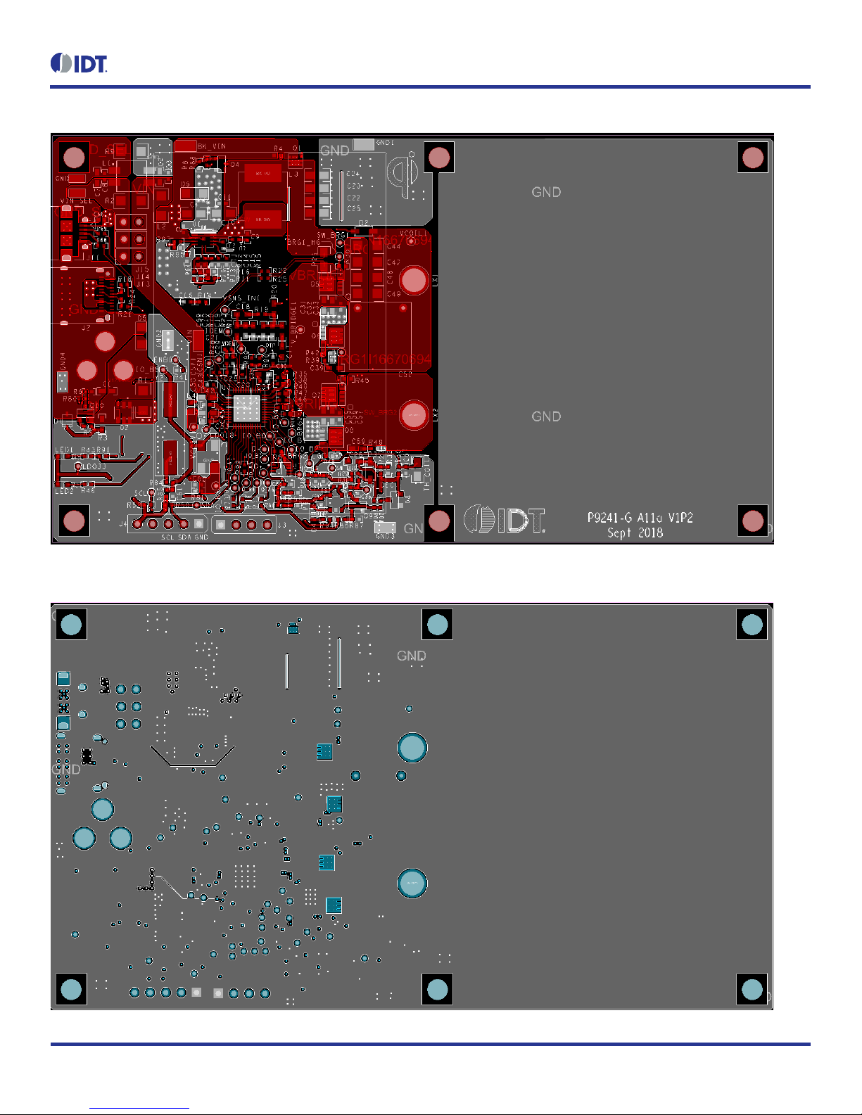
5. Board Layout ..............................................................................................................................................................................................17
6. Ordering Information...................................................................................................................................................................................20
7. Revision History..........................................................................................................................................................................................20
List of Figures
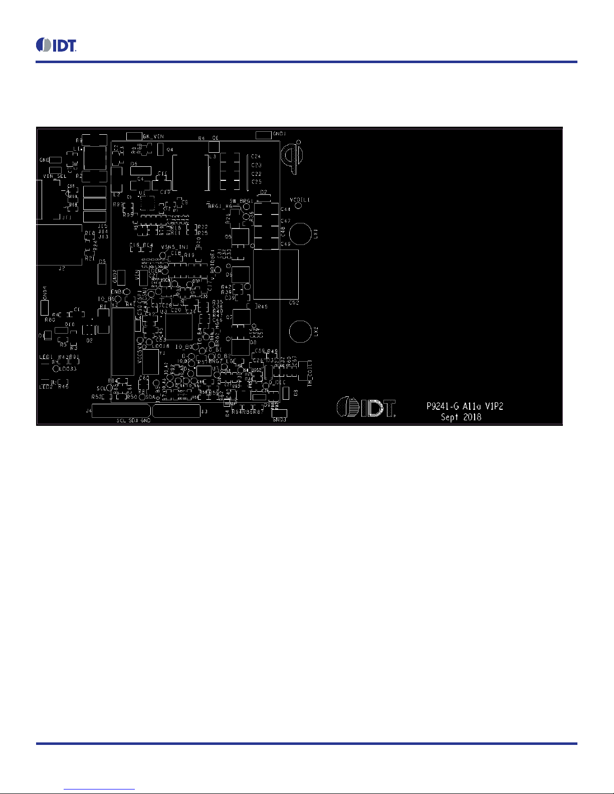
Figure 1. P9241-G V1.2 Evaluation Board Features ..........................................................................................................................................4
Figure 2. P9241-G V1.2 Evaluation Board Details..............................................................................................................................................5
Figure 3. R61 and R62 Location in the Schematic .............................................................................................................................................7
Figure 4. R61 and R62 PCB Location.................................................................................................................................................................7
Figure 5. TH_COIL1, R60, and RC67 Location in the Schematic.......................................................................................................................8
Figure 6. TH_COIL1, R60, and RC67 PCB Location..........................................................................................................................................8
Figure 7. Buck Regulator Location in the Schematic..........................................................................................................................................8
Figure 8. Buck Regulator PCB Location .............................................................................................................................................................9
Figure 9. Bypass Path Location in Schematic ....................................................................................................................................................9
Figure 10. Bypass Path PCB Location .................................................................................................................................................................9
Figure 11. Crystal Location in the Schematic .....................................................................................................................................................10
Figure 12. Crystal PCB Location ........................................................................................................................................................................10
Figure 13. Input Source Selection Jumpers on the PCB ....................................................................................................................................11
Figure 14. Silkscreen –Top of Board .................................................................................................................................................................17
Figure 15. Copper –Top Layer...........................................................................................................................................................................18
Figure 16. Copper –L1 Layer.............................................................................................................................................................................18
Figure 17. Copper –L2 Layer.............................................................................................................................................................................19
Figure 18. Copper –Bottom Layer .....................................................................................................................................................................19
List of Tables
Table 1. LED Pattern Selection .........................................................................................................................................................................6
Table 2. External Oscillator Selection..............................................................................................................................................................10
Table 3. Options for the Resonant Capacitor ..................................................................................................................................................11
Table 4. P9241-G-EVK Operation Modes .......................................................................................................................................................12
Table 5. Recommended Coil Manufacturers ...................................................................................................................................................12
P9241-G-EVK Evaluation Kit User Manual
© 2019 Integrated Device Technology, Inc.
4
March 1, 2019
1. Hardware Setup
Required or Recommended User Equipment
The following additional lab equipment is required for using the kit:
P9225-R-EVK Receiver Evaluation Board or any WPC-1.2.4 compliant receiver
Power supply capable of 5V, 9V, 12V, 16V to 19V/1.8A or the 12V/2.0A QC3.0 Quick Charge USB Wall Charger with the Micro-USB
Cable
2. Usage Guide
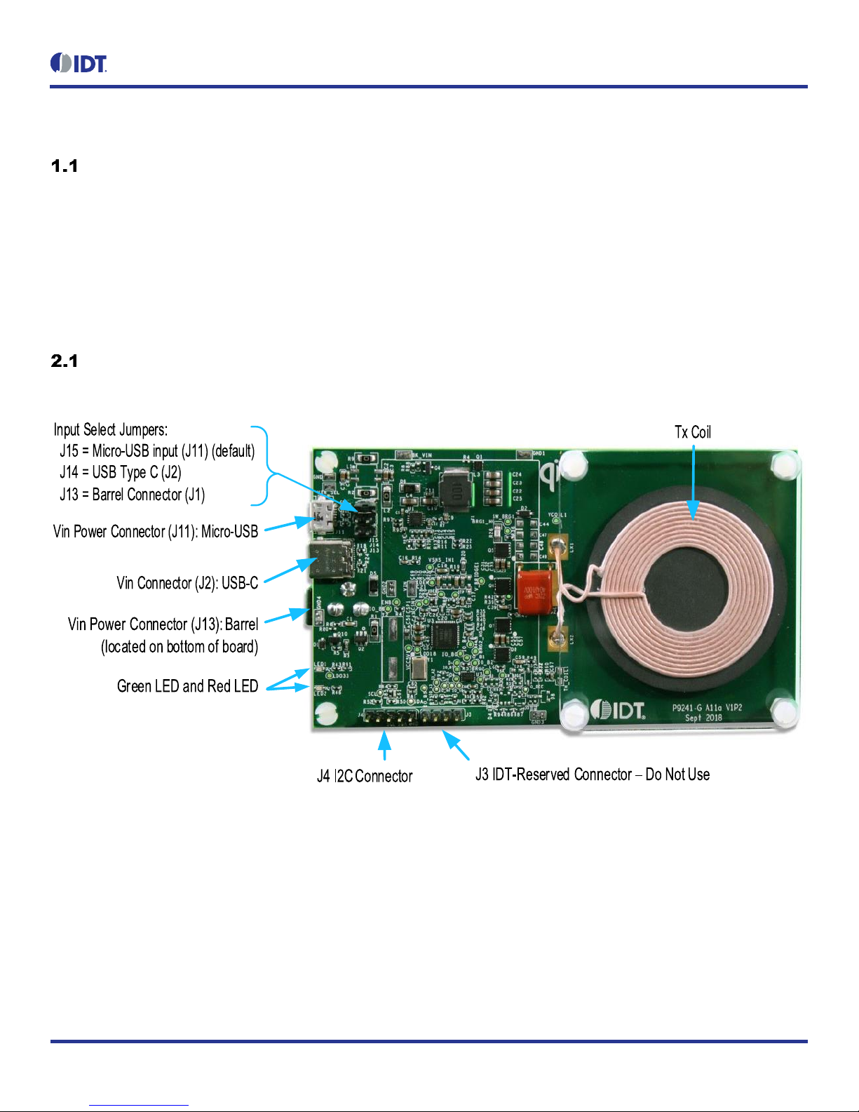
Overview of the P9241-G-EVK
Figure 1. P9241-G V1.2 Evaluation Board Features
P9241-G-EVK Evaluation Kit User Manual
© 2019 Integrated Device Technology, Inc.
5
March 1, 2019
Figure 2. P9241-G V1.2 Evaluation Board Details
P9241-GB IC
Buck Compensation Circuit
External Crystal
Buck IC Buck Power
Stage Filter
Film Resonance
Capacitor
High Voltage Input OVP Circuit
External Flash for
Development
Note: The P9241-GB IC is used instead of the production P9241-G IC on the P9241-G V1.2 Evaluation Board. The P9241-G IC has firmware
pre-programmed into the one-time programmable memory and does not allow users to customize the firmware. The P9241-GB also offers a
pre-programmed bootloader that must be used in conjunction with an external flash. Firmware is loaded into the external flash. Users can
customize the firmware in external flash. There is no functionality difference for the P9241-G V1.2 Evaluation Board using the P9241-G or the
P9241-GB with external flash.

P9241-G-EVK Evaluation Kit User Manual
© 2019 Integrated Device Technology, Inc.
6
March 1, 2019
LED Pattern Selection
The P9241-G-EVK uses two LEDs (LED1 and LED2 (see Figure 1) to indicate the power transfer status, faults, and operating modes. The LEDs
are connected to the LED1 and LED2 pins of the P9241-GB (see note below Figure 2) as shown in the P9241-G-EVK schematics.
The LED patterns can be selected by setting the voltage on the GPIO_A3 pin (see Table 1) via the resistor divider R61 and R62 (for location,
refer to Figure 3 and Figure 4). On the Evaluation Board, the GPIO_A3 pin is pulled down to GND through R62. R61 is unpopulated; therefore,
option 1 is the default option.
Table 1. LED Pattern Selection
Option
Voltage on GPIO_A3 Pin
LED1/LED2 Pin
Status
Standby
Transfer
Complete
Fault
1
0V ≤ VGPIO_A3 < 0.1V;
0.7V < VGPIO_A3 < 0.8V;
1.4V < VGPIO_A3 < 1.5V;
2.1V < VGPIO_A3 < 2.4V
LED2
Off
On
Off
Off
LED1
Off
Off
Off
Blink 4Hz
2
0.1V < VGPIO_A3 < 0.2V;
0.8V < VGPIO_A3 < 0.9V;
1.5 V< VGPIO_A3 < 1.6V
LED2
On
On
Off
Off
LED1
On
Off
Off
Blink 4Hz
3
0.2V < VGPIO_A3 < 0.3V;
0.9V < VGPIO_A3 < 1.0V;
1.6V < VGPIO_A3 < 1.7V
LED2
Off
Blink 1Hz
On
Blink 4Hz
LED1
Off
Off
Off
Off
4
0.3V < VGPIO_A3 < 0.4V;
1.0V < VGPIO_A3 < 1.1V;
1.7V < VGPIO_A3 < 1.8V
LED2
Off
On
Off
Blink 4Hz
LED1
Off
Off
Off
Off
5
0.4V < VGPIO_A3 < 0.5V;
1.1V < VGPIO_A3 < 1.2V;
1.8V < VGPIO_A3 < 1.9V
LED2
On
Blink 1Hz
On
Off
LED1
On
Off
Off
Blink 4Hz
6
0.5V < VGPIO_A3 < 0.6V;
1.2V < VGPIO_A3 < 1.3V;
1.9V < VGPIO_A3 < 2.0V
LED2
Off
Off
On
Off
LED1
Off
On
Off
Blink 4Hz
7
0.6V < VGPIO_A3 < 0.7V;
1.3V < VGPIO_A3 < 1.4V;
2.0V < VGPIO_A3 < 2.1V
LED2
Off
Blink 1Hz
On
Off
LED1
Off
Off
Off
Blink 4Hz

P9241-G-EVK Evaluation Kit User Manual
© 2019 Integrated Device Technology, Inc.
7
March 1, 2019
Figure 3. R61 and R62 Location in the Schematic
Figure 4. R61 and R62 PCB Location
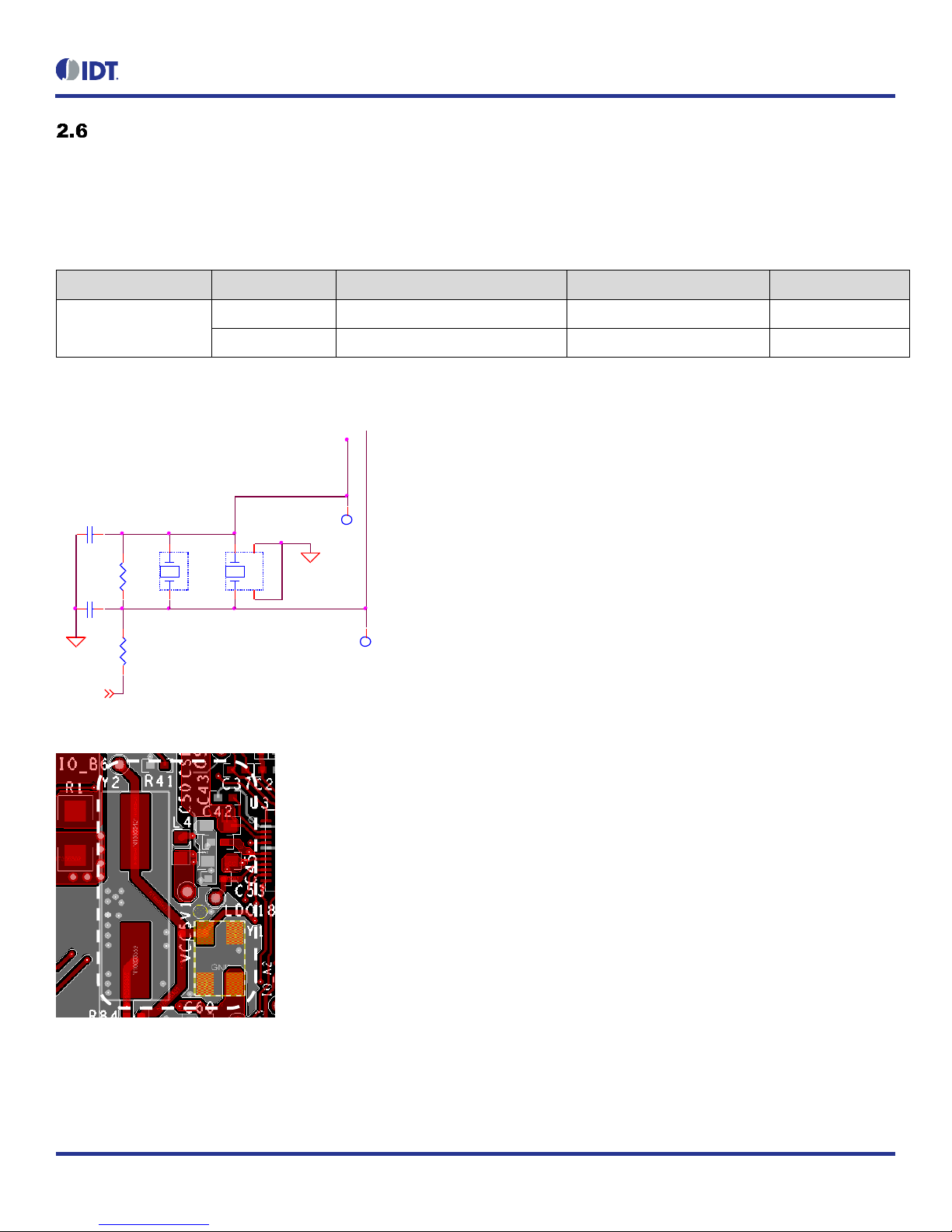
External Temperature Sensing (TS)
The P9241-G includes an optional temperature sense input pin, TS, that is used to monitor a remote temperature, such as for a coil or a battery
charger. The TS pin voltage can be calculated using Equation 1.
Where
NTC = The thermistor’s resistance (RTH1)
R60 = The pull-up resistor connected to the 3.3V supply voltage on the P9241-G Evaluation Board
Equation 1
The over–temperature shutdown is triggered if the voltage on the TS pin is lower than 0.6V and recovers at 0.8V. The RTH1 is not populated
on the P9241-G Evaluation Board.
FOD AND LED PAT
R58 20K R59 10k
R61 10K
FOD_ADJ
R62
10k
LDO33
LED_PAT

P9241-G-EVK Evaluation Kit User Manual
© 2019 Integrated Device Technology, Inc.
8
March 1, 2019
Figure 5. TH_COIL1, R60, and RC67 Location in the Schematic
Figure 6. TH_COIL1, R60, and RC67 PCB Location
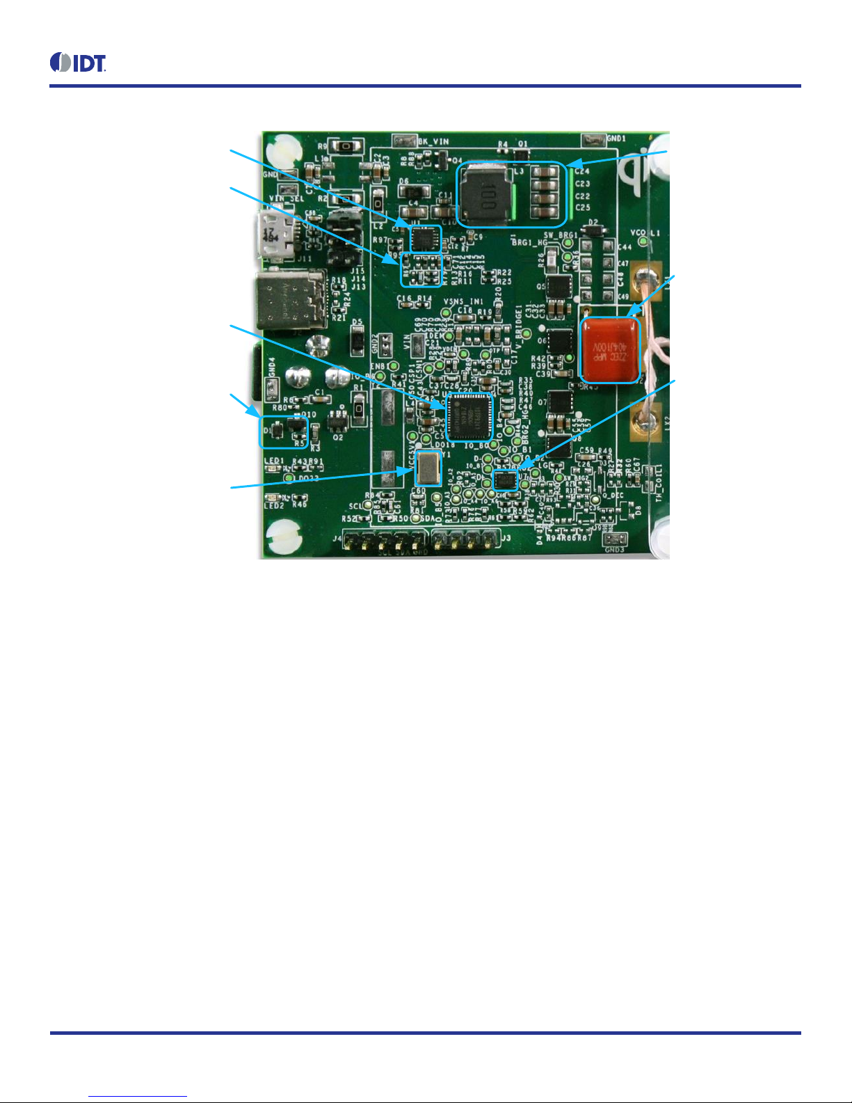
External Buck Regulator
To operate at a fixed 127.7kHz frequency, the P9241-G-EVK has adopted an MP2229 buck IC to adjust the power transfer between the
transmitter and receiver. GPIO_A4 and GPIO_B4 are assigned to adjust the MP2229 FB control. The MP2229 is operating at a fixed 500kHz
frequency on the board. The buck regulator power stage is designed to accommodate a wide range of input voltages. The feedback loop and
the external PWM signal are designed for the MP2229 and changing this circuit is not recommended. The resolution of the MP2229 is
approximately 35mV. The buck and external components in the PCB layout should be isolated from any noise generating circuits.
Figure 7. Buck Regulator Location in the Schematic
R60 10K
C67
0.1uF
OTP
OTP
t
TH_Coil1
COIL TEMPERATURE SENSING
LDO33
R13 18K
C10
22uF
R79
NP
R16
5.1K
BK_EN
C6
22uF
C11
0.1uF
BK_VIN
C14
NPC15
0.1uF
Q12
NP
C71 NP
C9 0.1uF
R96
0
R7 10
R11
150K
C4
22uF
R97
0
C12
0.1uF
C5
0.1uF
L3 10uH
BK_ADJ
R14 3.3K
BK_VIN
U1
MP2229
VCC
9
EN
4
LPM
5
FREQ/SYNC
8
BST 10
SW1 2
FB 6
SS 7
IN 3
SW2 11
GND1
1
INPAD 15
R67
0
C16
0.1uF
C13
NP
R12
30k
BK_FB
R95
10K
R66
NP
R15
30k
D6
SMAJ20CA-13-F
BK_SW

P9241-G-EVK Evaluation Kit User Manual
© 2019 Integrated Device Technology, Inc.
9
March 1, 2019
Figure 8. Buck Regulator PCB Location
Bypass Path of the External Buck Regulator
When the adaptor voltage is 5V only (such as for USB DCP or legacy USB 5V adaptors), the P9241-G-EVK supports such adaptors by turning
off the buck regulator and then enabling a bypass path. The P9241-G will be operating in a variable frequency mode to adjust the total power
transferred. GPIO_A4 is used to turn on the bypass path.
Figure 9. Bypass Path Location in Schematic
Figure 10. Bypass Path PCB Location
Q1
SIA453EDJ-T1_GE3
1
2
3
4
75
6
8
R88 0
BYPASS BUCK OPTIONAL:
NEEDED FOR 5V SUPPORT
R8
100k
R4
100k
BYP_EN
Q4
2N7002
P9241-G-EVK Evaluation Kit User Manual
© 2019 Integrated Device Technology, Inc.
10
March 1, 2019
External Crystal Circuit
To guarantee that the switching frequency is fixed at an accurate 127.7 kHz, two different types of crystals can be used to guarantee that the
frequency will be in the range defined in Table 2. Only one crystal is necessary; a choice can be made between the crystals designated as Y1
and Y2 in Table 2 by comparing cost and package size. By default, Y1 is populated on the P9241-G EVK board. GPIO_B6 and GPIO_B5 are
used to synchronize with the external crystal. Table 2 gives a list of the recommended devices for the crystal.
Table 2. External Oscillator Selection
Type
Vendor
Part Number
Typical Frequency (MHz)
Designator
Crystal
ECS, Inc.
ECS-80-18-30B-AGN-TR
8 (±50ppm)
Y1
Abracon, LLC
ABLS2-8.000MHZ-D4Y-T
8 (±50ppm)
Y2
Figure 11. Crystal Location in the Schematic
Figure 12. Crystal PCB Location
C61 18pF
R84
1M
LDO33
R85
10K
IO_B5
IO_B6
C60
18pF Y2
8MHz_NP
12
Y1
8MHz
13
24

P9241-G-EVK Evaluation Kit User Manual
© 2019 Integrated Device Technology, Inc.
11
March 1, 2019
Resonant Capacitor
The P9241-G-EVK can use four 100nF/100V/NPO/1206 capacitors as the resonant cap for best performance. For a lower cost solution, only
one film capacitor (400nF/100V or 250V) is used by default. For film capacitors used as the resonant capacitors, they must be carefully selected.
The important considerations include the following:
Metalized polypropylene type
High voltage rating
Stable DC characteristic
Stable AC characteristic; AC RMS rating de-rates based on operating frequency
Stable temperature characteristic; voltage rating degrades above 85°C, so it is better to use it at temperatures < 85°C
The ESR will be higher than that of 4 or 5 parallel C0G capacitors; therefore efficiency might be impacted
Table 3. Options for the Resonant Capacitor
Option
Resonant Capacitor
1
4 100nF, 100V, NPO, 1206
2 (low cost: < $0.2)
400nF; 100V or 250V; L8.6mm W10.3mm T3.5mm
Selection of Input Source and Operation Mode
The P9241-G-EVK supports different types of AD/DC adaptors and connectors. A shunt on the jumpers identified in Figure 13 can be used to
select the USB-Micro connector, USB-C connector, or DC jack adaptor. To select the proper jumper settings, refer to Figure 13.
Figure 13. Input Source Selection Jumpers on the PCB
P9241-G-EVK Evaluation Kit User Manual
© 2019 Integrated Device Technology, Inc.
12
March 1, 2019
The P9241-G-EVK supports a wide range of input DC sources from 5V to 19V. Based on the input source, the P9241-G-EVK supports different
types of receivers. Table 4 lists the P9241-G-EVK operation modes.
Table 4. P9241-G-EVK Operation Modes
Input Voltage(V)
Rx
Operating Frequency range(kHz)
5
BPP 5W (Bypass Buck)
110 to 148
9
BPP 5W (Buck)
110 to 148
Samsung AFC(10W)
110 to 148
iPhone 7.5W (Buck)
127.7
12
BPP 5W (Buck)
110 to 148
Samsung AFC 10W (Buck)
110 to 148
iPhone 7.5W (Buck)
127.7
16 to 19
BPP 5W (Buck)
110 to 148
Samsung AFC 10W (Buck)
110 to 148
iPhone 7.5W (Buck)
127.7
Transmitter Coil
The A11a coils in Table 5 are recommended for use with the P9241-G transmitter for optimum performance. The recommended vendor has
been tested and verified.
Table 5. Recommended Coil Manufacturers
Output Power
Vendor
Part Number
Inductance at 100kHz
Typical DCR at 25ºC
5W to 10W
SUNLORD
MQQTC505030S6R3
6.3µH
38mΩ
5W to 10W
CYNTEC
WTCL05054F-6R3ABKS-70
6.3µH
38mΩ

P9241-G-EVK Evaluation Kit User Manual
© 2019 Integrated Device Technology, Inc.
13
March 1, 2019
3. P9241-G Evaluation Board Schematic

P9241-G-EVK Evaluation Kit User Manual
© 2019 Integrated Device Technology, Inc.
14
March 1, 2019
4. Bill of Materials (BOM)
Table 3. P9241-G-EVK BOM
Item
Reference
Value
Description
Part Number
Manufacturer
Qty.
1
C1
0.1µF
CAP CER 0.1UF 25V X7R 0603
885012206071
Wurth Electronics Inc.
1
2
C2, C7, C31, C32, C35,
C42, C45, C55, C56
10µF
CAP CER 10UF 25V 20% X5R
0603
C1608X5R1E106M080AC
TDK
9
3
C3, C5, C8, C9, C11, C12,
C15, C16, C30, C33, C34,
C38, C46, C57, C66, C67,
C68, C75
0.1µF
CAP CER 0.1UF 25V 10% X7R
0402
CC0402KRX7R8BB104
Yageo
18
4
C4, C6, C10, C22, C23,
C24, C25
22µF
CAP CER 22UF 25V X5R 0805
GRM21BR61E226ME44
Murata Electronics
7
5
C18, C69
22nF
CAP CER 0.022UF 100V X7R
0603 CAP
C1608X7R2A223M080AA
TDK
2
6
C19
5.6nF
CAP CER 5600PF 100V X7R
0603
06031C562JAT2A
AVX Corporation
1
7
C20, 29
680p
CAP CER 680PF 50V X7R 0402
CL05B681KB5NNNC
Samsung Electro-
Mechanics
2
8
C21
22nF
CAP CER 0.022UF 25V X7R
0402
GRM155R71E223JA61D
Murata Electronics
1
9
C28
56pF
CAP CER 56PF 50V NP0 0402
CL05C560JB5NNNC
Samsung Electro-
Mechanics
1
10
C37, C43, C50, C53
1µF
CAP CER 1UF 25V 20% X5R
0402
CGB2A1X5R1E105M033BC
TDK
4
11
C39, C59
22nF
CAP CER 0.022UF 50V X7R
0603
GCM188R71H223KA37D
Murata Electronics
2
12
C44,C47,C48,C49
(Option 1)
100nF
CAP CER 100nF 100V C0G 1206
C3216C0G2A104J160AC
TDK
4
12
C52
(Option 2)
400nF
CAP CER 400nF 100V Film,
CBB21, L8.6mm W10.3mm
T3.5mm
CBB21-404J-100V
ZZEC Guangzhou
Zhongzheng Electronic
Development Co
1
13
C60, C61
18pF
CAP CER 18PF 50V C0G/NPO
0402
CC0402JRNPO9BN180
Yageo
2
14
D1
DDZ22ASF-7DICT
18.63~19.59V 300mW Zener,
DDZ22ASF
DDZ22ASF-7
Diodes Incorporated
1
15
D2
BAV21W
DIODE GEN PURP 80V 125MA
DFN, sod123
BAV21W
Diodes Incorporated
1
16
D5, D6
SMF20A-E3-08
TVS DIODE 20V 32.4V DO219AB
SMF20A
SMF20A-E3-08
Vishay
2
17
J1
AC_Adapter
CONN POWER JACK
2.5X5.5MM HI CUR
PJ-002AH
CUI Inc.
1
18
J2
USB Type C
USB Type C connector,
USB-C12401610E4
12401610E4#2A
Amphenol ICC
1

P9241-G-EVK Evaluation Kit User Manual
© 2019 Integrated Device Technology, Inc.
15
March 1, 2019
Item
Reference
Value
Description
Part Number
Manufacturer
Qty.
19
J3
SIP con
4 Positions Header, Unshrouded
Connector 0.100" (2.54mm)
Through Hole Gold or Gold,
GXT961104-6404-AR, sip-4
961104-6404-AR
3M
1
20
J4
68000-105HLF
BERGSTIK II .100" SR
STRAIGHT, sip5
68000-105HLF
Amphenol ICC
1
21
J11
5P
CONN RCPT MCR USB AB SMD
TH SHLL, usb_micro_ab
ZX62D-AB-5P8
1
22
LED1
LED
LED RED CLEAR 0603 SMD
150060RS75000
Wurth Electronics Inc.
1
23
LED2
LED
LED GREEN CLEAR 0603 SMD
150060GS75000
Wurth Electronics Inc.
1
24
L3
10µH
29mOhm, 3.6A inductor,
5x5-10x10
SWPA8040S100MT
SHENZHEN SUNLORD
ELECTRONICS
1
25
L4
4.7µH
FIXED IND 4.7UH 620MA 500
MOHM, L0603
CIG10W4R7MNC
Samsung Electro-
Mechanics
1
26
Q1
SIA453EDJ-
T1_GE3
MOSFET P-CH 30V 24A PPAK
SC-70-6, sc70_6ld_fet
SIA453EDJ-T1-GE3
Vishay Siliconix
1
27
Q2
Si3417
P-Channel 30 V , 35mOhm, 15nC
MOSFET, SOT-23-6
Si3417DV-T1-GE3
Vishay Siliconix
1
28
Q4
2N7002
N-Channel 60-V (D-S) MOSFET,
SOT23_3
2N7002KT1G
On Semiconductor
1
29
Q5, Q6, Q7, Q8
DMG7430LFG
MOSFET N-CH 30V 12A
PWRDI3333,
powerdi3333_8ld_fet
DMG7430LFG-7
Diodes Incorporated
4
30
Q10
MMBT4403/SOT
TRANS PNP 40V 0.6A, SOT23-3
MMBT4403-7-F
Diodes Incorporated
1
31
R1,R2,R9
0Ω
RES SMD 0.0 OHM JUMPER
1/4W 1206
RC1206JR-070RL
Yageo
3
32
R3
150Ω
RES SMD 150 OHM 1% 1/10W
0603
RC0603FR-07150RL
Yageo
1
33
R4,R8
100kΩ
RES SMD 100K OHM 1% 1/10W
0402
RC0402FR-07100KL
Yageo
2
34
R5, R19, R28, R58, R59,
R60, R61, R62, R85, R95
10kΩ
RES SMD 10K OHM 1% 1/10W
0402
RC0402FR-0710KL
Yageo
10
35
R6
91kΩ
RES SMD 91K OHM 1% 1/16W
0402
RC0402FR-0791KL
Yageo
1
36
R7
10Ω
RES SMD 10OHM 1% 1/10W
0402
RC0402FR-0710RL
Yageo
1
37
R11
150kΩ
RES SMD 150K OHM 1% 1/16W
0402
RC0402FR-07150KL
Yageo
1
38
R12, R15
30kΩ
RES SMD 30K OHM 1% 1/10W
0402
RC0402FR-0730KL
Yageo
2
39
R13
18kΩ
RES 18K OHM 1% 1/10W 0402
MCS04020C1802FE000
Vishay Beyschlag
1
40
R14
3.3kΩ
RES SMD 3.3K OHM 1% 1/16W
0402
RC0402FR-073K3P
Yageo
1
41
R16, R50, R52
5.1kΩ
RES SMD 5.1K OHM 1% 1/10W
0402
ERJ-2RKF5101X
Panasonic
3
P9241-G-EVK Evaluation Kit User Manual
© 2019 Integrated Device Technology, Inc.
16
March 1, 2019
Item
Reference
Value
Description
Part Number
Manufacturer
Qty.
42
R20
2.4kΩ
RES SMD 2.4K OHM 1% 1/10W
0603
RC0603FR-072K4L
Yageo
1
43
R22, R25
10Ω
RES SMD 10 OHM 1% 1/10W
0402
ERJ-2RKF10R0X
Yageo
2
44
R23
200kΩ
RES SMD 200K OHM 1% 1/10W
0603
RC1608F204CS
Samsung Electro-
Mechanics
1
45
R26
0.02Ω
RES SMD 0.02 OHM 1% 1/3W
0805
UCR10EVHFSR020
Rohm Semiconductor
1
46
R35, R40, R44, R47
22Ω
RES SMD 22 OHM 5% 1/10W
0402
ERJ-2GEJ220X
Panasonic Electronic
Components
4
47
R36, R42, R45, R48, R57
100kΩ
RES SMD 100K OHM 5% 1/10W
0402
ERJ-2GEJ104X
Panasonic Electronic
Components
5
48
R41, R43
1kΩ
RES SMD 1K OHM 5% 1/16W
0402
RC0402JR-071KL
Yageo
2
49
R46
680Ω
RES SMD 680 OHM 5% 1/16W
0402
RC0402JR-07680RL
Yageo
1
50
R18, R21, R39, R49, R67,
R68, R69, R73, R76, R77,
R80, R88, R90, R97
0Ω
RES SMD 0 OHM JUMPER
1/16W 0402
RC0402JR-070RL
Yageo
14
51
R84
1MΩ
RES SMD 1M OHM 5% 1/16W
0402
RC0402JR-071ML
Yageo
1
52
U1
MP2229
Buck Converter Chip, QFN-14
(3X3), MP_2229
MP2229GQ
Monolithic Power Systems
Inc.
1
53
U3
P9241-GB
Medium Power Transmitter,
socketqfn_48_6x6_0p4
P9241-GB
IDT
1
54
U7
W25X40CLUXIG
IC FLASH 4M SPI 104MHZ
8USON, uson_2x3_8LD
W25X40CLUXIG
Winbond Electronics
1
55
Y1
8MHz
CRYSTAL 8MHZ 18PF SMD,
ECX-53B
ECS-80-18-30B-AGN-TR
ECS Inc.
1
P9241-G-EVK Evaluation Kit User Manual
© 2019 Integrated Device Technology, Inc.
17
March 1, 2019
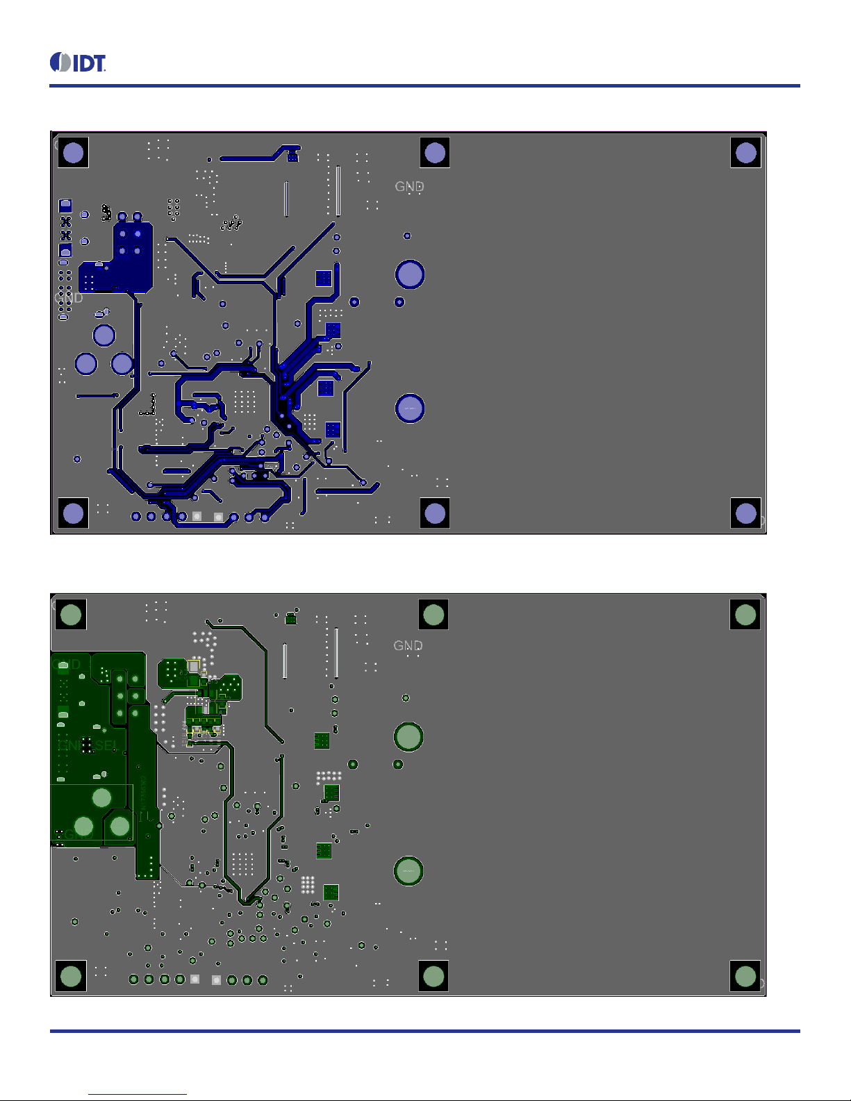
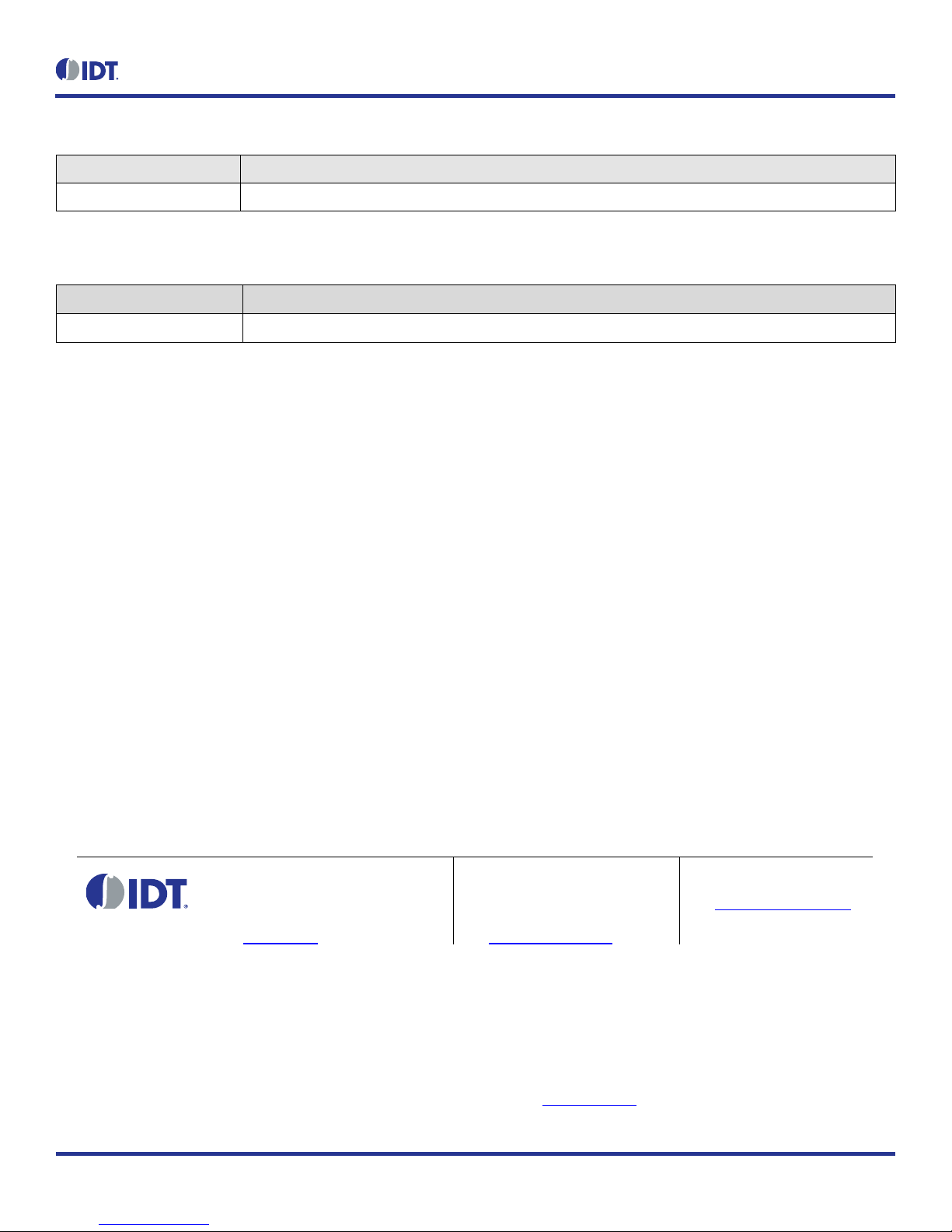
5. Board Layout
Figure 14. Silkscreen –Top of Board
P9241-G-EVK Evaluation Kit User Manual
© 2019 Integrated Device Technology, Inc.
18
March 1, 2019
Figure 15. Copper –Top Layer
Figure 16. Copper –L1 Layer
P9241-G-EVK Evaluation Kit User Manual
© 2019 Integrated Device Technology, Inc.
19
March 1, 2019
Figure 17. Copper –L2 Layer
Figure 18. Copper –Bottom Layer
P9241-G-EVK Evaluation Kit User Manual
© 2019 Integrated Device Technology, Inc.
20
March 1, 2019
6. Ordering Information
Orderable Part Number
Description
P9241-G-EVK
P9241-G-EVK Evaluation Board, 12V/2.0A QC3.0 Quick Charge USB Wall Charger, and Micro-USB cable.
7. Revision History
Revision Date
Description of Change
March 1, 2019
Initial release.
Corporate Headquarters
6024 Silver Creek Valley Road
San Jose, CA 95138
www.IDT.com
Sales
1-800-345-7015 or 408-284-8200
Fax: 408-284-2775
www.IDT.com/go/sales
Tech Support
www.IDT.com/go/support
DISCLAIMER Integrated Device Technology, Inc. (IDT) and its affiliated companies (herein referred to as “IDT”) reserve the right to modify the products and/or specifications described herein at any time,
without notice, at IDT's sole discretion. Performance specifications and operating parameters of the described products are d etermined in an independent state and are not guaranteed to perform the same
way when installed in customer products. The information contained herein is provided without representation or warranty of a ny kind, whether express or implied, including, but not limited to, the suitability
of IDT's products for any particular purpose, an implied warranty of merchantability, or non -infringement of the intellectual property rights of others. This document is presented only as a guide and does not
convey any license under intellectual property rights of IDT or any third parties.
IDT's products are not intended for use in applications involving extreme environmental conditions or in life support systems or similar devices where the failure or malfunction of an IDT product can be
reasonably expected to significantly affect the health or safety of users. Anyone using an IDT product in such a manner does so at their own risk, absent an express, written agreement by IDT.
Integrated Device Technology, IDT and the IDT logo are trademarks or registered trademarks of IDT and its subsidiaries in the United States and other countries. Other trademarks used herein are the
property of IDT or their respective third party owners. For datasheet type definitions and a glossary of common terms, visit www.idt.com/go/glossary. All contents of this document are copyright of Integrated
Device Technology, Inc. All rights reserved.
Table of contents
Other IDT Motherboard manuals

IDT
IDT 5P49V5907 Manual

IDT
IDT 8A34xxx 48QFN series User manual

IDT
IDT PhiClock 9FGV1001 User manual

IDT
IDT VersaClock 5 User manual

IDT
IDT ZMOD4510-EVK User manual

IDT
IDT 8T49N24 Series Installation and operating instructions

IDT
IDT ZSSC41 Series User manual

IDT
IDT Tsi340-RDK1 User manual

IDT
IDT ZMOD4410 User manual

IDT
IDT EB-LOGAN-23 User manual

IDT
IDT 89EBPES16T4G2 User manual

IDT
IDT Tsi381 User manual

IDT
IDT ZMID520 Series User manual

IDT
IDT EB8T5A Eval Board User manual

IDT
IDT 9FGV1005 Operating instructions

IDT
IDT 89EBPES12N3 User manual

IDT
IDT ZNRG2061 User manual

IDT
IDT EB4T4 Eval Board User manual

IDT
IDT ZSSC4151 User guide

IDT
IDT 8T49N240 User manual


