Kirisun DP405 User manual

DP405
V190409 ShenZhen Kirisun Communications Co.,Ltd.
Professional wireless communication system solution supplier
SERVICE MANUAL

DP405 Service Manual
Contents
1.Overview ......................................................................................................................................................1
1.1. Scope.....................................................................................................................................................1
1.2. Safety Precautions.................................................................................................................................1
1.3. Maintenance Service.............................................................................................................................1
2.External View and Operation Description................................................................................................2
2.1. External View.........................................................................................................................................2
2.2. Operation Description............................................................................................................................2
2.3. LED Indication .......................................................................................................................................3
2.4. Basic Operation.....................................................................................................................................4
3.Circuit Description......................................................................................................................................4
3.1. Circuit Composition................................................................................................................................4
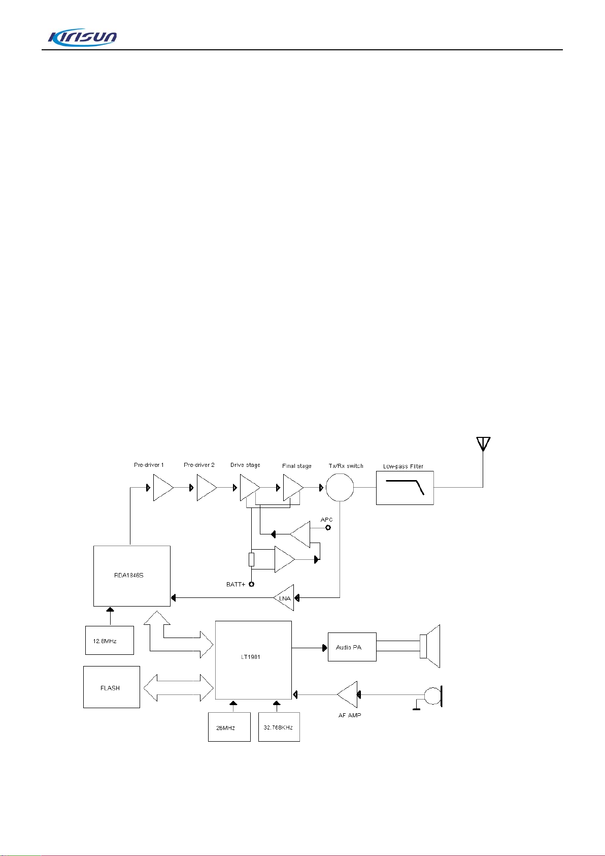
3.2. TX Circuit...............................................................................................................................................5
3.3. RX Principle...........................................................................................................................................5
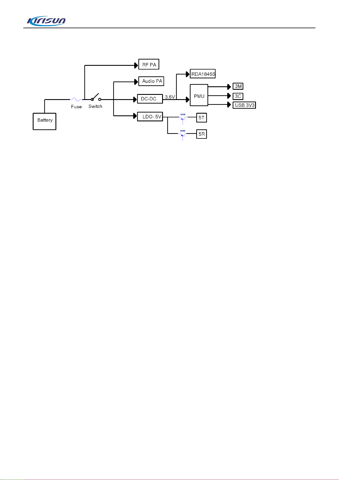
3.4. Power Section........................................................................................................................................6
3.5. IC Description........................................................................................................................................6
3.6. Semiconductor Device Description .......................................................................................................7
3.6.1. MCU Description.................................................................................................................................7
3.6.2. RDA1846S Port Description.............................................................................................................10
3.7. Semiconductor Device Feature Description.........................................................................................11
4.Feature Description and Parameter Setting ..........................................................................................12
4.1. Kill and Remote Monitor......................................................................................................................12
4.2. Scan.....................................................................................................................................................13
4.3. Zone.....................................................................................................................................................13
4.4. Setting..................................................................................................................................................13
4.5. TOT (Time-out-timer).....................................................................................................................14
4.6. Emergency Alarm ................................................................................................................................14
4.7. Feature Setting....................................................................................................................................15
5.Attaching and Detaching..........................................................................................................................15
5.1. Attaching and Detaching the Battery...................................................................................................15
5.2. Attaching and Detaching theAntenna.................................................................................................16
5.3. Installing the Earphone........................................................................................................................16
5.4. Detaching the Housing from the Chassis (see figure below)..............................................................17
5.5. Detaching the Motherboard from the Chassis (see figure below)....................................................18
5.6. Exploded View.....................................................................................................................................19
6.Modulation and Test.................................................................................................................................21
6.1. Method.................................................................................................................................................21
6.1.1. Components needed for adjustment.................................................................................................21
6.1.2. PC Test Mode Modulation Method:...................................................................................................21
6.2. Radio Test............................................................................................................................................21
7.Main Technical Performance and Specification....................................................................................22
8.Maintenance and Test Equipment...........................................................................................................23
9.Troubleshooting........................................................................................................................................24
Appendix 1 Abbreviations ........................................................................................................................26
I

DP405 Service Manual
Appendix 2 Material List(electronic section)........................................................................................27
List 1 DP405-02 Motherboard material list..................................................................................................27
List 2 DP405-01 Motherboard Material List.................................................................................................38
List 3 Module List............................................................................................................................................51
Appendix 3 Material List (Structural Section)...........................................................................................53
Appendix 4 Accessory List..........................................................................................................................57
Appendix 5 Schematic Disagram and Postion Mark................................................................................58
Diagram 1 DP405-02 Motherbaord Schematic Diagram (6PM7-4169-HMB).............................................58
Diagram 2 DP405-02 Motherboard Position Mark (6PM7-4169-HMB).......................................................63
Diagram 3 DP405-01 Motherbaord Schematic Diagram (6PM7-4169-HMB).............................................65
Diagram 4 DP405-01 Motherbaord Postion Mark (6PM7-4169-HMB)........................................................70
Diagram 5 Module Schematic Diagram (6PD7-4038-HL1G)......................................................................72
Diagram 6 Module Postion Mark (6PD7-4038-HL1G).................................................................................78
Appendix 6 Schematic Disagram and Postion Mark................................................................................79
Diagram 1 DP405-02 Motherbaord Schematic Diagram (6PM7-4169-HMF).............................................79
Diagram 2 DP405-02 Motherboard Position Mark (6PM7-4169-HM F)......................................................84
Diagram 3 DP405-01 Motherbaord Schematic Diagram (6PM7-4169-HMF).............................................86
Diagram 4 DP405-01 Motherbaord Postion Mark (6PM7-4169-HMF)........................................................91
Diagram 5 Module Schematic Diagram (6PM7-4320-HBA)........................................................................93
Diagram 6 Module Postion Mark (6PM7-4320-HBA) ..................................................................................99
II

DP405 Service Manual
1.Overview
1.1.Scope
This manual is intended for maintenance and repair of DP405 portable radio, and can only be used by
engineers and professional technicians who are trained by Kirisun. The parameters in this manual may vary
with technology improvement, so for updated technical information, please contact Kirisun or its local
dealers.
Please carefully read this manual before repairing the radio.
1.2.Safety Precautions
Electromagnetic Radiation
Radios generate and radiate electromagnetic energy. The security design of Kirisun radio meets national
and international standards on electromagnetic radiation. To ensure radio’s optimal performance and safe
electromagnetic radiation on human, please keep the radio vertical to the ground and 2-5 cms away from
your mouth.
Electromagnetic Interference
To avoid electromagnetic interference, please turn off the radio wherever there are clear warnings, e.g.
hospitals, health care centers, airports and other places where radios must be turned off.
Explosive and Harmful Gases
The radio should be turned off in areas where there are explosives and harmful gases, e.g. lower deck of
the hull, fuel and chemical storage facilities and area where the air contains chemicals, particles, dust or
metal dust.
Please turn off the radio when close to blasting area and electric blasting detonators.
Replacing or charging batteries in potentially explosive atmosphere is prohibited.
Antenna Damage
Do not use radios when the antenna is damaged. Damaged antenna may cause mild burning to human
skin.
Replacing Components
When replacing components, please be aware of the model number. Do not arbitrarily replace any
components that do not match Kirisun’s requirement.
1.3.Maintenance Service
The radio and accessory are provided with warranty service. But if one of the following occurs, no free
maintenance is offered.
No valid warranty card or original invoice.
1

DP405 Service Manual
Faults caused by unauthorized disassembly, repair and modification.
Man-made damage such as wear, mechanical damage, burning, and waterlogging.
Product serial number is damaged or the product brand is unable to identify.
After the warranty expired, lifetime service is still available. We also provide service components to service
station and staff at favorable price.
2.External View and Operation Description
2.1. External View
No. Part Name No. Part Name
1 Mic Jack 2 Model Sticker
3 Antenna 4 Channel Knob
5 Volume Knob 6 Guide Beam
7 Logo Sticker 8 Mic
9 Speaker 10 PTT Key
11 Programmable Key 12 Belt Clip
13 Battery 14 Battery Clip
2.2. Operation Description
The programmable keys can be set as long press feature key or short press feature key according to user’s
2

DP405 Service Manual
requirements. The available features are listed below:
No. Feature Usage
1 None No feature
2 High/low Power Press this key to switch high/low power.
3 Broadcast Call Press this key to make a broadcast call.
4 Monitor
If there is CTCSS on the current analogue channel, press this key to
switch to carrier squelch mode to cancel CTCSS feature. When the
carrier is matched, the voice can be output. Press the key again to
go back to the original status.
5 EmergencyAlarm Enable the emergency alarm feature to seek help in emergency.
6 Eemrgency Alarm Exit End emergency alarm.
7 Squelch on/off P
ress this key on the analogue channel to forcibly open the voice
reception path and receive weak signals on the analogue
channel. Pressing this key on digital channel is useless.
8 Zone Selection Press this key to switch to the next zone.
9 Scan
Press this key to enable Scan and listen to activities on other
channels; press it again to disable Scan.
10 Alert Tone on/off
Press this key to enabel all the alert tones and press it again to have
them disabled.
11 Niusance Delete Durng scan, when the radio detects an unnecessary channel, e.g.
interference channel, the user can select Nuisance Delete menu to
delete the channel before the scan continues.
12 Repeater/Talkaround On the repeater channel, press this key to exit repeater mode.
2.3.LED Indication
LED Indication Radio Status
Red LED glows The radio is transmitting
Red LED flashes The radio is in low power.
Green LED Glows The radio is receiving signals (voice, data) or detects activity on
channel
Green LED flashes The radio is scanning
Orange LED flashes The radio is in call hang status or receiving emergency alarm.
3

DP405 Service Manual
2.4.Basic Operation
Power on/off the Radio
When the radio is off, turn the volume knob clockwise until a click is heard to power on the radio; when the
radio is on, turn the volume knob counter-clockwise until a click is heard to power off the radio.
Selecting the Channel
Turn the channel knob to select the channel.
Adjusting the Volume
Turn the volume knob to adjust the volume.
Initiaing a Call
Press PTT key and speak to the mic.
Receiving
When the radio receives the signal which matches the current channel, it will output the voice on channel.
3.Circuit Description
3.1.Circuit Composition
4

DP405 Service Manual
3.2.TX Circuit
The TX circuit is mainly composed of three parts below:
RF PowerAmplification Circuit
RDA1846S outputs RF signal from pin 18 and enters first-level pre-drive amplifier (Q502) for initial
amplification; then it enters second-level pre-drive amplifier (Q503)and drive amplifier (Q501) for further
power amplification, ensuring sufficient drive power signal can be offered to final amplifier for ultimate
power amplification; after amplification by multiple amplifiers, the transmitted signal will complete the output
impedance match at the output terminal of final power amplifier through a section of microstripe, so as to
minimize output power loss from impedance match failure; afterwards, the transmitted signal will enter the
low pass filter through TX/RX switch.
Low Pass Filter Circuit
The low pass filter which suppresses harmonic wave is an advanced Chebyshev filter composed of lumped
parameter inductor and capacitor. On a certain basis of in-band fluctuation, the filter can improve
suppression to out-of-band harmonic wave and spurious signal.
Automatic Power Control Circuit (APC)
In the automatic power control circuit, the drain current from drive power amplifier and final power amplifier
completes switch from current to voltage through the sampling resistor and subtraction circuit which is
made of the first operational amplifier; the voltage will be compared with the APC control voltage output
from DAC at the second operational amplifier, and the error voltage that is output will change the
transmitting power through the grid bias voltage of the control power amplifier tube (including the drive level
and final level ).
3.3.RX Principle
The RX circuit is mainly composed of RF low pass filter, RX/TX switch, low noise amplifier, RDA1846S,
LT1901 and audio power amplifier.
RX Circuit Front-end
The signal from antenna is sent to Q507 3SK318 and low noise amplifier (LNA) which is made of peripheral
components though RX/TX switch for amplification, and the amplified signal will then be sent to U500
(RDA1846S)for demodulation and output.
RX Circuit Back-end
The analogue/digital signal which is demodulated and output by RDA1846S, after completing demodulation
and processing of digital signal through DSP in LT1901, will be input to digital audio processor module for
further processing, and then be switched to analogue voice signal through DAC of codec; the analogue
voice signal will finally be amplified by external audio amplifier to drive the speaker.
5

DP405 Service Manual
3.4.Power Section
The radio applies 7.4V lithium-ion battery for power supply. RF power amplification and audio power
amplification are directly powered by battery; the battery outputs 3.6V to supply power to PMU in
RDA1846S and LT1901 through DC-DC switch; 3M, 3C and USB3.3V output from PMU separately
supply power to other baseband circuits; the battery outputs 5V voltage through LDO and then outputs
separate 5T and 5R after control by Q100 and Q102.
RF PA:RF PowerAmplifier Circuit Q500(RD07MUS2B), Q501(RD01MUS2)
Audio PA: Audio Power Amplifier Circuit U3(TDA8547TS)
3M:EEPROM IC200(AT24C512C), encrypted IC U2(LTJMIC)
3C:Transistor X500(12.8M TCXO)
5T:RF Pre-driveAmplifer Circuit Q502 (2SC5108)、 Q503(2SC3356)
5R:Low Noise High FrequencyAmplifier Circuit Q507(3SK318)
DC-DC:PMU IC1(LT1901)、 U500(RDA1846S)
3.5.IC Description
RDA1846S Feature:
Fully-integrated CMOS RF Front-end
High Linearity Low NoiseAmplifer and Mixer
Low IF Receiver Path
Auomatic DC offset Calibration Circuit
High Performance analogue/digital converter and digital/analogue converter
Fully-integrated Receiver Filter
Digital AGC
Modulation and demodulation technique based on digital signal processing technique
6

DP405 Service Manual
TX Path of Direct Frequency Synthesis
Modulation Method of Direct Frequency Synthesis
TX Filter based on Digital Signal Processing Technique
TX Modulation Gain Number is Adjustable
Digital voice activates TX control
High-performance Fractional PLL Frequency Synthesizer
Fully-integrated In-chip RF VCO
Fully-integrated Internal Loop Filter
Low Phase Noise
Fast Lock of Phase
High-frequency Resolution with Random FrequencyAdjustable
Built-in Transistor Frequency Error Calibration Circuit
Sleep Mode of Ultra Low Loss
Three Wire Serial Digital Interface Control
3.6.Semiconductor Device Description
3.6.1. MCU Description
Pin No. Port No. Port Name Definition
E11 GPIO_D44 JM_RST Encrypted IC Reset
J19 BSENS MAND_IN Upside down IC level input
L22 ADC_IN BAT_DET Battery power check
W13 GPIO_D7 PF Side key input
R14 GPIO_D6 BEEP_C Received voice\alert tone switch control
W14 GPIO_D101 EERROM_WP EEPROM
AA17 GPIO_D24 ECN_3 Channel switch
AB17 GPIO_D23 ECN_2 Channel switch
V15 GPIO_D11 KEYPAD5 4*4 key
V16 GPIO_D99 KEYPAD3 4*4 key
V17 GPIO_D100 MAND_C Upside down IC power supply control
7

DP405 Service Manual
AA18 GPIO_D22 EXT_PTT External PTT
U18 GPIO_D98 KEYPAD2 4*4 key
V19 GPIO_D96 KEYPAD0 4*4 key
U19 GPIO_D13 KEYPAD7 4*4 key
T19 GPIO_D14 NC_GPIO NC
U21 GPIO_D12 KEYPAD6 4*4 key
T21 GPIO_D97 KEYPAD1 4*4 key
V22 GPIO_D10 KEYPAD4 4*4 key
F5 GPIO_D112 LCD_RS LCD
AB19 LCD_CS1 LCD_RST LCD
L21 SSI0_RX SSI0_RX FLASH
P21 SSI0_TX SSI0_TX LCD/FLASH
N21 SSN0 LCD_CS LCD
M21 SSN1 FLASH_CS FLASH
F6 GPIO_D111 NC NC_GPIO
R21 SSI0_CLK SSI0_CLK LCD/FLASH
A12 VOUT_D9 VIO_3V_C PMU_3V output
J14 GPIO_D76 UART_RXD0 Serial port 0
J15 GPIO_D75 UART_TXD0 Serial port 0
F22 BAT_DET BAT_DET Battery check
J18 GPIO_D25 UART_TXD1 Serial port 1
H18 GPIO_D26 UART_RXD1 Serial port 1
E17 GPIO_D74 TONE_OUT Alert tone PWM output
E18 VSB BATTERY Clock button battery access
E21 SINK1 NC NC
D23 SINK2 NC NC
C18 GPIO_D88 I2C_SDA EEPROM
A17 VOUT_D2 3M PMU_3M output
C17 GPIO_D87 I2C_SCL EEPROM
8

DP405 Service Manual
E14 GPIO_D49 NC NC
C14 GPIO_D51 AFCO1 Audio power amplification MUTE
E13 GPIO_D48 5TC 5TC
A13 VOUT_D3 3C PMU_3C output
C13 GPIO_D52 DACS_SW1 DA_MCP4802
B13 GPIO_D47 5RC 5RC
E12 GPIO_D50 LDAC_PC/TV DA_MCP4802
C12 GPIO_D53 AFCO2 Speaker output MUTE
A11 GPIO_D46 RDA_PDN RDA1846S
A10 GPIO_D58 SPI/CS RDA1846S
F11 GPIO_D2 NC_GPIO
B11 GPIO_D57 SPI/CLK RDA1846S
B10 GPIO_D56 SPI/DA_OUT RDA1846S
F10 GPIO_D0 RDA_SQL SQL
E10 GPIO_D3 KEYPAD_BL Backlight control
K18 GPIO_D107 JM_CLK New encrypted IC
B9 GPIO_D21 ECN1 Channel switch
A8 GPIO_D18 GREEN_LED Green light control
B8 GPIO_D16 PTT PTT
A7 GPIO_D19 NC_GPIO
B7 GPIO_D20 ECO_0 Channel switch
C7 GPIO_D17 RED_LED Red light control
C3 AUX_OUTP SPK+ Audio output after LT1901 demodulation
D3 AUX_OUTN SPK- NC
D1 M_MICP AFDET RDA1846S is sent to LT1901 after
demodulation
D2 M_MICN NC NC
E2 HP_MICN MIC1 MIC signal is sent to LT1901
H5 DM USB_DM USB
J5 DP USB_DP USB
9

DP405 Service Manual
L1 HPL_OUT MOD1 Digital MIC signal output
M1 HPR_OUT MOD2 NC
D21 SINK3 NC_SINK3 NC
B12 GPIO_D45 JM_SDATA Encrypted IC
C11 GPIO_D55 NC_GPIO NC
A9 GPIO_D59 APC_SW2 APC_SW2
C9 GPIO_D105 NC_GPIO NC
C8 GPIO_D43 APC_SW1 APC_SW1
F15 GPIO_D8 NC_GPIO NC
F14 GPIO_D9 QT/DQT IN QT/DQT IN
F13 GPIO_D1 LCD_BL LCD backlight control
3.6.2. RDA1846S Port Description
AVDD 1 Power supply
SCLK 2 Clock input for serial control bus
SDIO 3 Data input/output for serial control bus
AVDD 4 Power supply
XTAL1 5 Oscillator pin 1
XTAL2 6 Oscillator pin 2,control interface select
MODE 7 When MODE = VL, I2C Interface is select; When MODE = VH, SPI
Interface is select
SENB 8 Latch enable (active low) input for serial control bus
AFOUT 9 Audio signal output to speaker
NC* 10 No connection
MIC_IN 11 MIC input
Cc 12 Compensation capacitor connection
AVDD 13 Power supply
NC* 14 No connection
10

DP405 Service Manual
RFIN 15 RF signal input
AVDD 16 Power supply
NC* 17 No connection
RFOUT 18 RF signal output
NC* 19 No connection
NC* 20 No connection
AVDD 21 Power supply
PABIAS 22 PA bias supply for PA
AVDD 23 Power supply
PDN 24 Chip enable,high active; Chip sleep,low active
GPIO7 25 Gpio7/vox(When Gpio7=VH, vox is active; else VL)
GPIO6
26 Gpio6 / sq
(When Gpio6=VH, sq is active; else VL)
GPIO5
27 Gpio5 / txon
(When Gpio5=VH, txon is active; else VL)
GPIO4
28 Gpio4 / rxon
(When Gpio4=VH, rxon is active; else VL)
GPIO3
29
Gpio3 / sdo
(Gpio3=VH or VL, it is the output register data in 4 wire control
Interface mode)
GPIO2
30 Gpio2 / int
(When Gpio2=VH, int is active; else VL)
GPIO1
31 Gpio1 / code_in / code_out
(Gpio1=VH or VL, it is the input/output code data)
GPIO0
32 Gpio0 / css_in / css_out
(Gpio0=VH or VL, it is the input/output CTCSS/CDCSS signal)
3.7.Semiconductor Device Feature Description
Position Mark MODEL Description
IC500 NJM2904 APC,voltage comparison, drive
11

DP405 Service Manual
U21 LT1901A MCU
IC200 24LC512 E2PROM,
saves channel frequency data, feature parameters and
modulation parameters
U3 TDA8547TS Receiver audio power amplification
Q500 RD07S2B TX final power amplification
Q4 DTA144EE APC output switch
Q507 3SK318 Receiver power amplifier
Q200 DTC144EE Red LED driver
Q201 DTC144EE Green LED driver
Q501 RD01MUS1 Transmitter power amplifier drive
Q601 DTC144EE Audio power amplifier control switch
IC100 XC6204B50
2MR 5R,5T voltage output
IC102 MP2359 3.5V voltage DC-DC output
U20 MCP4802 DA chip, used for modulation of power and frequency stability
Q602 Q603 ST3400SRG Audio output control switch
IC302 NJM2904 Operational amplifier IC, used for MIC signal amplification
Q502 2SC5108 Transmitter 1st amplification
Q503 2SC3356 Transmitter 2st amplification
4.Feature Description and Parameter Setting
4.1.Kill and Remote Monitor
Kill
Check this option to receive Kill command and the radio will be disabled.
Kill Decode
Check this option to receive Revive command and the radio will be restored to normal.
Remote Monitor
When the radio receives Remote Monitor command, it will automatically turn on the transmitting and the
monitoring party can listen to the surroundings around the monitored radio.
12

DP405 Service Manual
4.2. Scan
Enabling Scan
Press the Scan programmable key to enable Scan and listen to activities on other channels. Press Scan
key again to exit Scan.
Scan List
Each channel can be related to one “Scan List” though dealer programming. The radio can only start Scan
on channels related with “Scan List”. Each “Scan List” contains a maximum of 16 channels (including the
current channel), both analogue channels and digital channels can be contained. By selecting “Scan List”
menu, you can check the scan channels included in the “Scan List” used by the current channel.
Note:
if the scan channels in the list are changed, other channels which are related with the same list will be
affected during channel scan.
Nuisance (Temporary) Delete
During scan, when the radio stops on an unnecessary channel, e.g. intereference channel, it can select
Nuisance Delete to delete this channel before it goes on scanning. You can also add a temporary channel
during scan.
After exiting scan mode, the channel which is temporarily deleted or added will turn invalid.
Scanning the Revert Channel
During radio scan, press the PTT key to enable the radio to transmit or talk on the preset channel. This
channel can be set by local dealer using programming software.
4.3.Zone
A group of available channels can compose a zone. The zone can be selected through programmable key.
4.4.Setting
You can set the radio parameters according to personal requirements. The parameters include power,
squelch level, whisper, auto keypad lock, alert tone, home screen display, power-saving mode, language,
voice intensificaton, vice encryption and etc.
Power
High power enables communication of longer distance but leads to shorter battery use while lower power
enables communication of shorter distance but leads to longer battery use. The power level of each
channel can be separately set.
Squelch Level
The squelch is leveled from 0 to 9, and higher level means smaller interference from noise or other
unnecessary signals but it is difficult to receive weak signals.
13

DP405 Service Manual
Whisper
Enable Whisper and talk to the mic, and the called party can hear the voice clearly.
Alert Tone
The aler tone can be set by PC software and you can enable/disable all kinds of alert tone.
Power-saving mode
Enable/disable the power-saving mode, which extends the battery use duration
Voice Encryption
Enable/diable Voice Encryption feature on the current channel.
4.5.TOT (Time-out-timer)
This feature prevents long occupation on the channel. If the continuous transmitting time exceeds the
preset time, the radio will stop tranmistting and sound alert tone. To stop the alert tone, please release the
PTT key. For the next transmitting, please press the PTT key after a certain interval (set by dealer). If the
pre-alert feature is enabled by dealer, a pre-alert will sound right before the TOTtime, indicating the coming
tramission limit.
4.6.Emergency Alarm
Press Emergency Alarm programmable key during emergency. The emergency alarm is composed of two
parts: alarm type, which specifies voice and sound reaction during emergency, and alarm mode, which
specifies the transmission contents sent to other members during emergency. To disable emergency alarm,
please press emergency alarm exit shortcut key.
Alarm Type:
None: no alarm feature (default);
Siren Only: only sounds alarm on the radio;
Conventional: sounds alarm with voice and light alert and other radio response can be received;
Secret: no voice or light alert and it cannot receive response from other radios;
Secret with voice: no voice or light alert but it can receive response from other radios.
Alarm Mode:
Emergency Alarm: after the alarm is initiated, the radio sends only emergency alarm. It exits the alarm
status afterwards.
Emergency Alarm+Emergency Call: the radio sends emergency alarm but also sends emergency call if
PTT key is pressed.
Emergency Alarm + Background Tone Auto Transmission: the radio sends emergency alarm and also
sends automatic background tone periodically.
14

DP405 Service Manual
Note:
Emergency Alarm: the radio sends a kind of non-speech signal to trigger alarm on other radios.
Emergency Call: a kind of call mode with higher priority than other conventional calls, which ensures
fluent call during emergency.
4.7.Feature Setting
The radio will be pre-set before delivery, but due to different requirements by users, parameters such as
digital features, working frequency, channels, QT/DQT, auto scan or others may be re-set. Kirisun designed
user-friendly programming software with easy operation to program DP405.
Programming procedures is listed as follows:
A.Install DP405 programming software;
B.Use a programming cable to connect the radio and PC.
For detailed instruction, please refer to Help file in the programming software and DP405 user guide.
5.Attaching and Detaching
This radio is a sophisticated communication device with precise and compact structure. Please be careful
with the repair.
5.1.Attaching and Detaching the Battery
Detaching the Battery
Make sure the radio is turned off when detaching the battery.
Push the battery latch in the direction as ①shows; the radio will pop up as ②shows; press the belt clip as
④shows to detach the battery.
PC
Programming Cable
Radio
15

DP405 Service Manual
Attaching the Battery
Press ①to pop up the belt clip, and align the battery with the aluminum shell to insert the battery in the
direction as ②shows; press the bottom of battery until it is locked.
Note:
Please do not throw the battery terminal or battery into fire.
Do not take the liberty of taking out the battery shell.
5.2.Attaching and Detaching the Antenna
To attach the antenna, insert the antenna on the top of the radio and turn it clockwise until it is fastened;
To detach the antenna, turn it counter-clockwise to loosen it.
5.3.Installing the Earphone
Open the cover board on the right side of the radio, and insert the earphone plug into the interface.
16

DP405 Service Manual
5.4.Detaching the Housing from the Chassis (see figure
below)
(1) Detach the antenna;
(2) Detach the two knobs and circlips;
(3) Detach the two knob nuts and antenna nut;
(4) Detach the two screws as shown below;
(5) Insert a flat screwdriver into the aluminum bracket and pry the bracket; take out the bracket and take
out the soft flat cables.
17
Other manuals for DP405
2
Table of contents
Other Kirisun Portable Radio manuals

Kirisun
Kirisun TP66001 User manual

Kirisun
Kirisun TP620 User manual

Kirisun
Kirisun PT6500 User manual

Kirisun
Kirisun TP620 User manual

Kirisun
Kirisun PT260 User manual

Kirisun
Kirisun TP620 User manual

Kirisun
Kirisun DP770 User manual

Kirisun
Kirisun FP560-01 User manual

Kirisun
Kirisun W60 User manual

Kirisun
Kirisun DP990 User manual