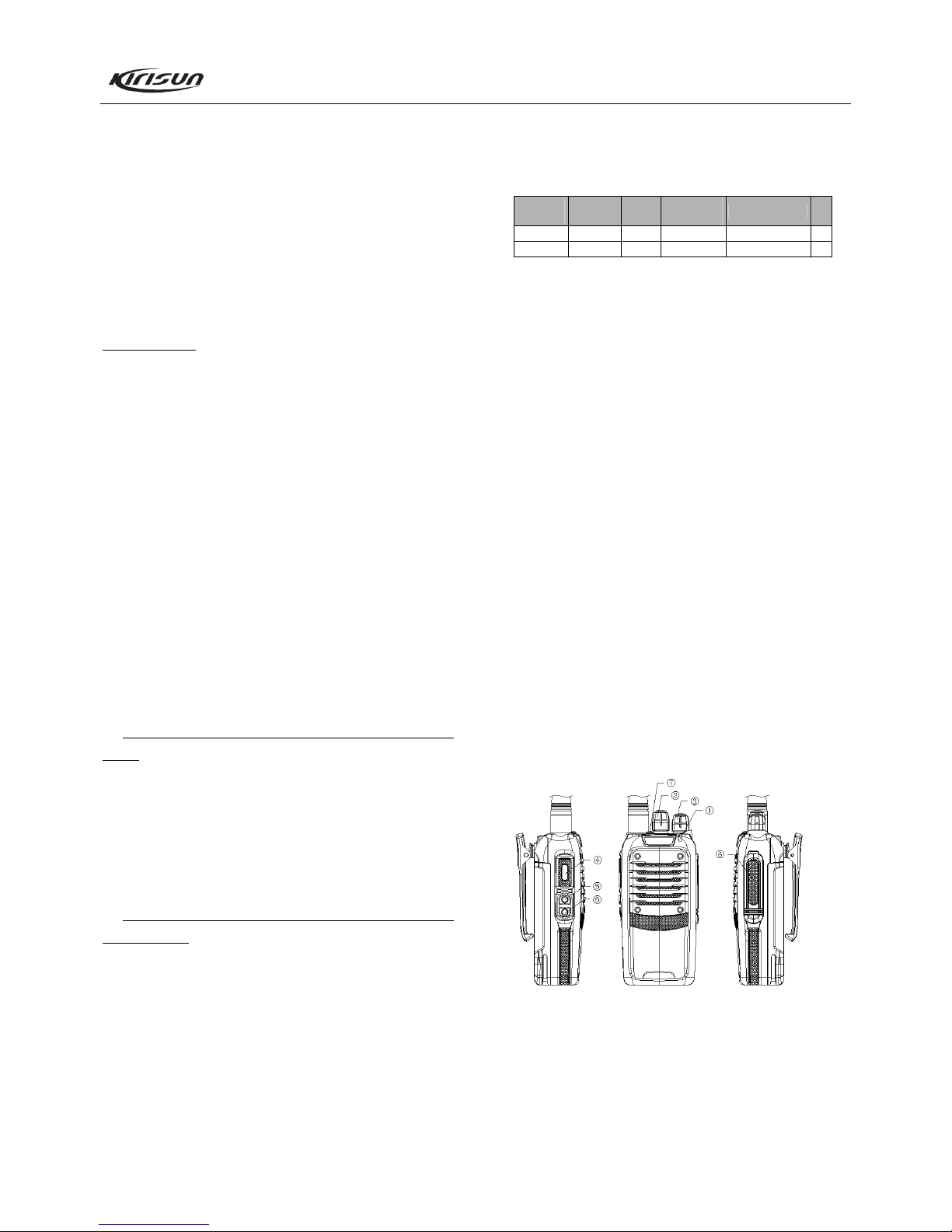
PT568 Service Manual
5
The Tx voice signal processing circuit consists of IC7 and its
peripheral components. After being amplified, limited and filtered,
the voice signal from MIC is sent to VCO for modulation together
with CTCSS/DCS signal.
The AGC circuit consists of D13, D308 and Q24. When signal
from MIC is too large, the AGC circuit will lower the signal
strength to make sure that no distortion happens to the signal.
Q34 is the power switch of the voice processing circuit. It is
controlled by MCU. Power supply of IC7 will be turned on when
the radio is transmitting.
J2 is the jack for external MIC. When using external MIC, the
internal MIC will be turned off automatically. But the internal
PTT is still effective.
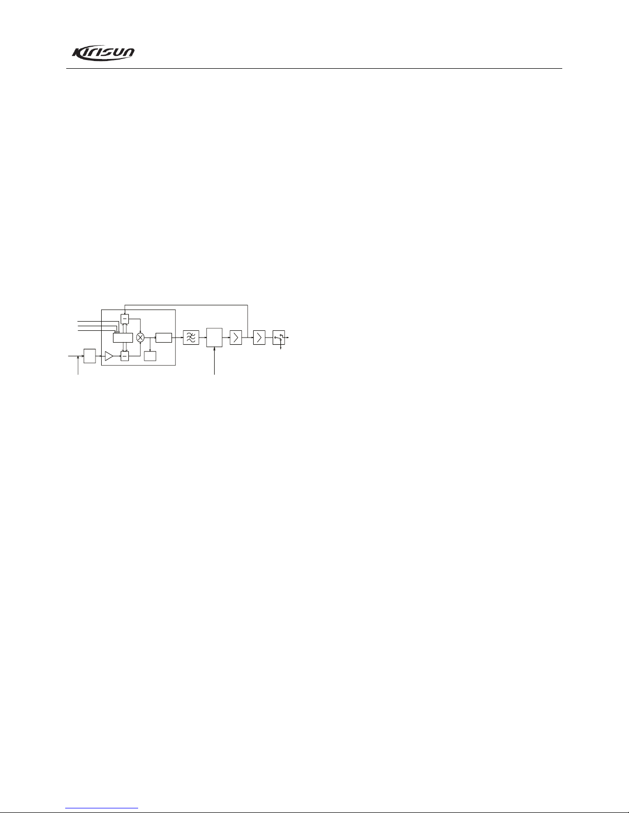
3.4 Principle of Frequency Synthesizer
1
Nr
1
N
Control Circuit Charge
UL
Detect
Pump
TCXO
DCS Mod
Freq Adj
to MCU VCCN
Data
CK
LE
to MCU
VCO
RX
TX
D3,D6
Q4
Q5
MOD in
Figure 3.8 Frequency Synthesizer
The radio adopts PLL type frequency synthesizer.
The frequency synthesizer consists of reference oscillator,
voltage control oscillator (VCO), programmable divider, phase
comparator, and low pass filter.
Rx VCO unit consists of Q14, L30, C120, C88, C142, C180,
D8 and D9. Tx VCO unit consists of Q15, L51, C121, C137,
C206, C194, D10 and D11. D12 is the modulation circuit of VCO.
IC1 (MB15E03) is PLL integrated circuit, which consists of
programmable reference divider, programmable swallowing
divider, phase comparator, and charge pump.
The low pass filter consists of R244, C193, R202, R40, C207,
R141, C205, R2 and C204. The reference frequency is provided
by X4 (TCXO, 12.8MHz).
The reference frequency from TCXO (Temperature
Compensated Crystal Oscillator) is divided by the programmable
reference divider in IC1 to produce reference frequency of 5kHz
or 6.25kHz (determined by the preset channel frequency and is
controlled by MCU).
The oscillation frequency from VCO goes to IC1 where it is
divided by the programmable swallowing divider and is then
compared with the reference frequency to obtain error signal. The
signal is then filtered by a low pass filter and is sent to VCO to
change the oscillation frequency of the VCO, enabling the
frequency to reach the set value. Then the VCO is locked.
N=F
VCO/FR
N: Times of frequency division
F
VCO: Oscillation frequency of VCO
F
R: Reference frequency
Unlock detection: When PLL is unlocked, Pin 14 of IC will
output low level signal to MCU. Then MCU prohibits the
transmitter from transmitting and makes an alert tone.
Q6: Power filter, which provides more purified power for PLL
to reduce noise of the frequency synthesizer.
3.5 Voice Alert Circuit
The radio is provided with voice alert function, which is
especially useful at night or in dark environment.
IC15 is a voice memory chip, which is stored with voices of
channel indication etc. Once the channel selector knob is switched,
the speaker will announce the current channel number. You can
press the preprogrammed “Voice Alert” key to repeat the current
channel number.
If voice alert function is enabled, the speaker will announce
the current channel number once the “Voice Alert” key is pressed
under standby mode. You can switch the voice type by pressing
and holding the “Voice Alert” key while restarting the radio. Do it
repeatedly to switch the voice type in the order of “Chinese
Male-English Male-Chinese Female-English Female-No Alert”.
3.6 Power Supply
The radio uses 7.4V, 1700mAh Li battery. The Tx power
amplification circuit (Q11 and Q12) and the Rx audio power
amplifier (IC8) directly adopt the battery for power supply. Power
of other circuits is supplied by 5V regulated voltage.
IC12: 5V low dropout, micro-power regulator, which supplies
5V power with large current for the radio together with Q10 and
Q30.
Q29: 5T switch, which is controlled by MCU.
5T: Supplies power for front end of Tx.
Q31: 5R switch, which is controlled by MCU.
5R: Supplies power for RF amplifier, mixer, IF processing unit,
and audio signal processing unit etc. of the receiver.
Q32: 5C switch, which is controlled by MCU.
5C: 5V power supply under SAVE control. Supplies power for
frequency synthesizer.
3.7 MCU Unit