Chapter 1:
Introduction
Thank you for choosing LVC-2001. The fanless Box PC is
an ideal vehicle gateway controller. LVC-2001 is built with
Intel® Atom™ E3845/E3825 CPU, that supports 4 processor
cores and operates with DDR3L SO-DIMM memory up
to 4GB. The compact and fanless form factor make it
suitable for vehicle applications. Regarding environmental
reliability, LVC-2001 is certied with MIL-STD-810G
vibration and shock resistance. As a vehicle computing
system, LVC-2001 is designed with GPS and G-sensor I/O
for navigation purpose. Other useful I/Os include 2 x RJ-45
LAN ports, 3 mini-PCIe expansion slots with 4 SIM card
sockets, 2 serial ports, 1 optional CAN bus, 2 USB ports and
+9~36VDC power input.
Features:
Intel• ® Atom™ E3845 / E3825 CPU
1 x DDR3L SODIMM max up to 4 GB memory•
2 x Intel® 10/100/1000 Mbps RJ-45 ports•
2 x full-size mini-PCIe slots and 1 x half-size mini PCIe•
slot with total 4 external accessible SIM slots support
Wi-Fi/3G/4G(LTE)/mSATA
MIL-STD-810G vibration/shock resistance•
Display: 1 x VGA and 1 x HDMI•
USB: 1 x USB 3.0 type-A and 1 x USB 2.0 type-A•
Onboard GPS receiver module and G-sensor•
COM ports: 2 x RS-232/422/485 with RI/5V/12V•
Optional: CAN bus support J1939 / J1708•
System Specifications
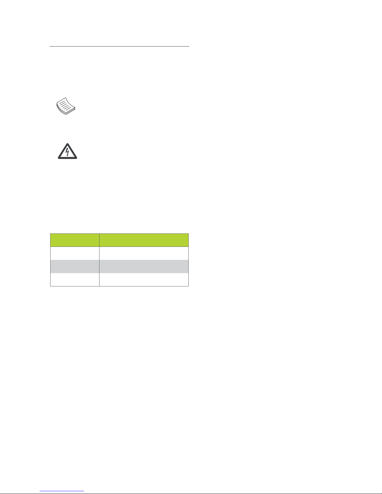
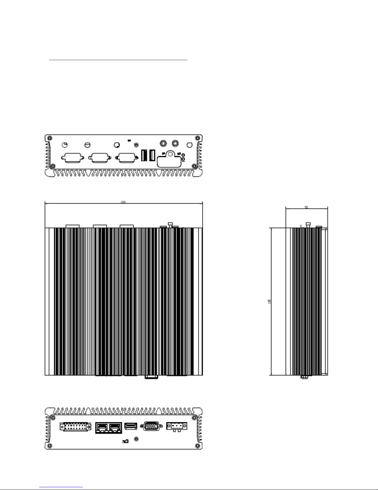
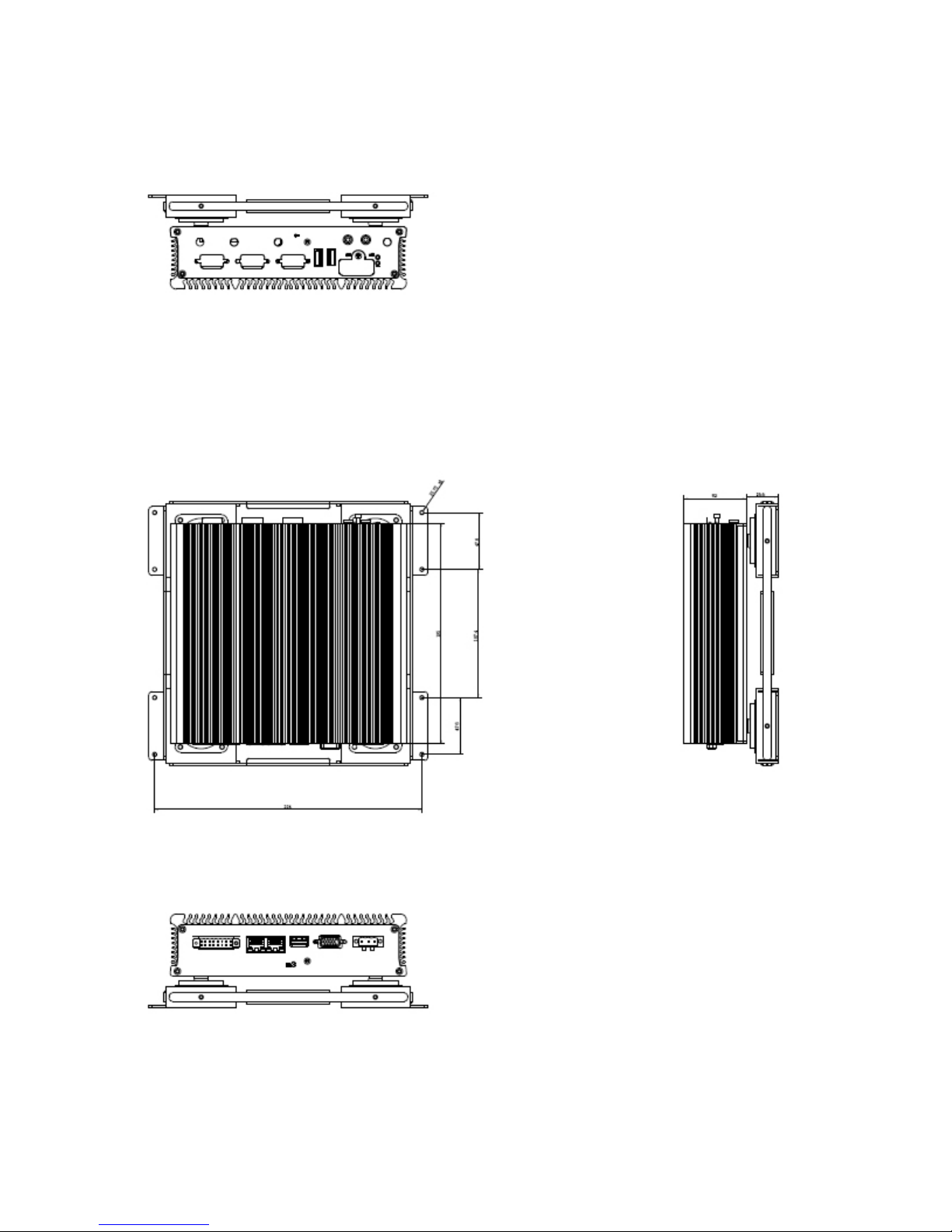
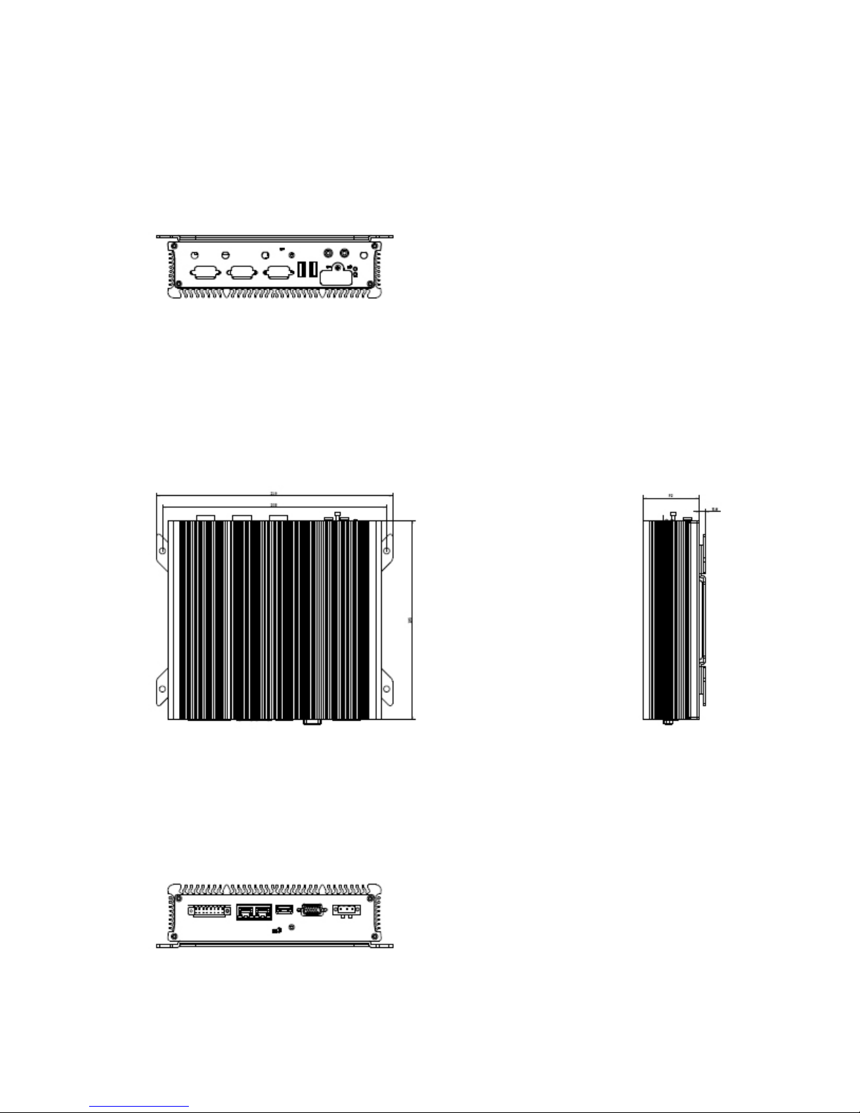
Dimensions
198 x 52 x 185 (mm, the unit)
Processor Intel® BayTrail E3845/E3825
System Memory DDR3L SO-DIMM x1 (up to 4GB)
BIOS AMI SPI Flash BIOS
Storage mSATA/SATA 1 x mSATA socket
1 x SATA 2.5” 9.5 mm drive bay
Ethernet Controller 2 x Intel® i210-IT
Graphic Controller
Intel HD Graphics
Audio Mic IN/Line OUT
I/O
LAN 2 x RJ45 at 10/100/1000 Mbps
Display 1 x VGA
1 x HDMI
Serial I/O COM1/2: 2 x DB9 RS-232/422/485
with RI/5V/12V
GPS u-blox NEO-7N
G-sensor ADXL 345
USB 1 x USB 3.0 Type A
1 x USB 2.0 Type A
Power Input
3-pin terminal block (+,-,ignition),
+9~36VDC,
ATX mode support ignition delay
on/ off control
Expansion
2x Full-size mini-PCIexpress socket
(1x USB+PCIe+2xSIM; 1x USB+2
x SIM )
1x half-size mini-PCIexpress socket
CAN bus supports J1939 & J1708, (module
optional)
MIO
4x DI (5V or 12V TTL selectable)
4x DO (12V TTL , Max. 100mA)
2x MCU DI
1x 12V Output @Max. 1A
Power
Input 3-pin terminal block (+,-,ignition),
+9~36VDC,
Output 12V/1A DC out
Adaptor Optional
Environment Operating
Temperature
-20~60°C (with industrial-grade
components)
-5~45°C (without industrial-grade
components)
Humidity 5% ~ 95%, non-condensing
Mechanical System Design Fanless
Weight 1.8 kg
Mounting Wallmount or suspension kit
Certication EMC CE/FCC Class A, E13, RoHS
Reliability Compliance
Vibration: MIL-STD-810G, Method
514.6
Shock: MIL-STD-810G, Method
516.6
OS Support Windows Windows: WES7 (WS7E) / W7 Pro
SP1 / WE8 STD
Linux Linux Kernel 2.6.18 or later