LG 55LH85 - - 54.6" LCD TV User manual

TV COM1 COM2AV1 AV2 R GB
WIRELESS
1 2 3 4
4
LCD TV
SERVICE MANUAL
CAUTION
BEFORE SERVICING THE CHASSIS,
READ THE SAFETY PRECAUTIONS IN THIS MANUAL.
CHASSIS : LA92F
MODEL : 55LH85 55LH85-UC
North/Latin America http://aic.lgservice.com
Europe/Africa http://eic.lgservice.com
Asia/Oceania http://biz.lgservice.com
Internal Use Only
Printed in KoreaP/NO : MFL58600436 (0905-REV00)

Copyright LG Electronics. Inc. All right reserved.
Only for training and service purposes - 2 - LGE Internal Use Only
CONTENTS
CONTENTS ............................................................................................. 2
PRODUCT SAFETY ................................................................................. 3
SPECIFICATION....................................................................................... 6
ADJUSTMENT INSTRUCTION .............................................................. 10
EXPLODED VIEW .................................................................................. 16
SVC. SHEET ...............................................................................................

Copyright LG Electronics. Inc. All right reserved.
Only for training and service purposes - 3 - LGE Internal Use Only
SAFETY PRECAUTIONS
Many electrical and mechanical parts in this chassis have special safety-related characteristics. These parts are identified by in the
Schematic Diagram and Exploded View.
It is essential that these special safety parts should be replaced with the same components as recommended in this manual to prevent
Shock, Fire, or other Hazards.
Do not modify the original design without permission of manufacturer.
General Guidance
An isolation Transformer should always be used during the
servicing of a receiver whose chassis is not isolated from the AC
power line. Use a transformer of adequate power rating as this
protects the technician from accidents resulting in personal injury
from electrical shocks.
It will also protect the receiver and it's components from being
damaged by accidental shorts of the circuitry that may be
inadvertently introduced during the service operation.
If any fuse (or Fusible Resistor) in this TV receiver is blown,
replace it with the specified.
When replacing a high wattage resistor (Oxide Metal Film Resistor,
over 1W), keep the resistor 10mm away from PCB.
Keep wires away from high voltage or high temperature parts.
Before returning the receiver to the customer,
always perform an AC leakage current check on the exposed
metallic parts of the cabinet, such as antennas, terminals, etc., to
be sure the set is safe to operate without damage of electrical
shock.
Leakage Current Cold Check(Antenna Cold Check)
With the instrument AC plug removed from AC source, connect an
electrical jumper across the two AC plug prongs. Place the AC
switch in the on position, connect one lead of ohm-meter to the AC
plug prongs tied together and touch other ohm-meter lead in turn to
each exposed metallic parts such as antenna terminals, phone
jacks, etc.
If the exposed metallic part has a return path to the chassis, the
measured resistance should be between 1MΩand 5.2MΩ.
When the exposed metal has no return path to the chassis the
reading must be infinite.
An other abnormality exists that must be corrected before the
receiver is returned to the customer.
Leakage Current Hot Check (See below Figure)
Plug the AC cord directly into the AC outlet.
Do not use a line Isolation Transformer during this check.
Connect 1.5K/10watt resistor in parallel with a 0.15uF capacitor
between a known good earth ground (Water Pipe, Conduit, etc.)
and the exposed metallic parts.
Measure the AC voltage across the resistor using AC voltmeter
with 1000 ohms/volt or more sensitivity.
Reverse plug the AC cord into the AC outlet and repeat AC voltage
measurements for each exposed metallic part. Any voltage
measured must not exceed 0.75 volt RMS which is corresponds to
0.5mA.
In case any measurement is out of the limits specified, there is
possibility of shock hazard and the set must be checked and
repaired before it is returned to the customer.
Leakage Current Hot Check circuit
1.5 Kohm/10W
To Instrument’s
exposed
METALLIC PARTS
Good Earth Ground
such as WATER PIPE,
CONDUIT etc.
AC Volt-meter
IMPORTANT SAFETY NOTICE
0.15uF

Copyright LG Electronics. Inc. All right reserved.
Only for training and service purposes LGE Internal Use Only
- 4 -
CAUTION: Before servicing receivers covered by this service
manual and its supplements and addenda, read and follow the
SAFETY PRECAUTIONS on page 3 of this publication.
NOTE: If unforeseen circumstances create conflict between the
following servicing precautions and any of the safety precautions on
page 3 of this publication, always follow the safety precautions.
Remember: Safety First.
General Servicing Precautions
1. Always unplug the receiver AC power cord from the AC power
source before;
a. Removing or reinstalling any component, circuit board
module or any other receiver assembly.
b. Disconnecting or reconnecting any receiver electrical plug or
other electrical connection.
c. Connecting a test substitute in parallel with an electrolytic
capacitor in the receiver.
CAUTION: A wrong part substitution or incorrect polarity
installation of electrolytic capacitors may result in an
explosion hazard.
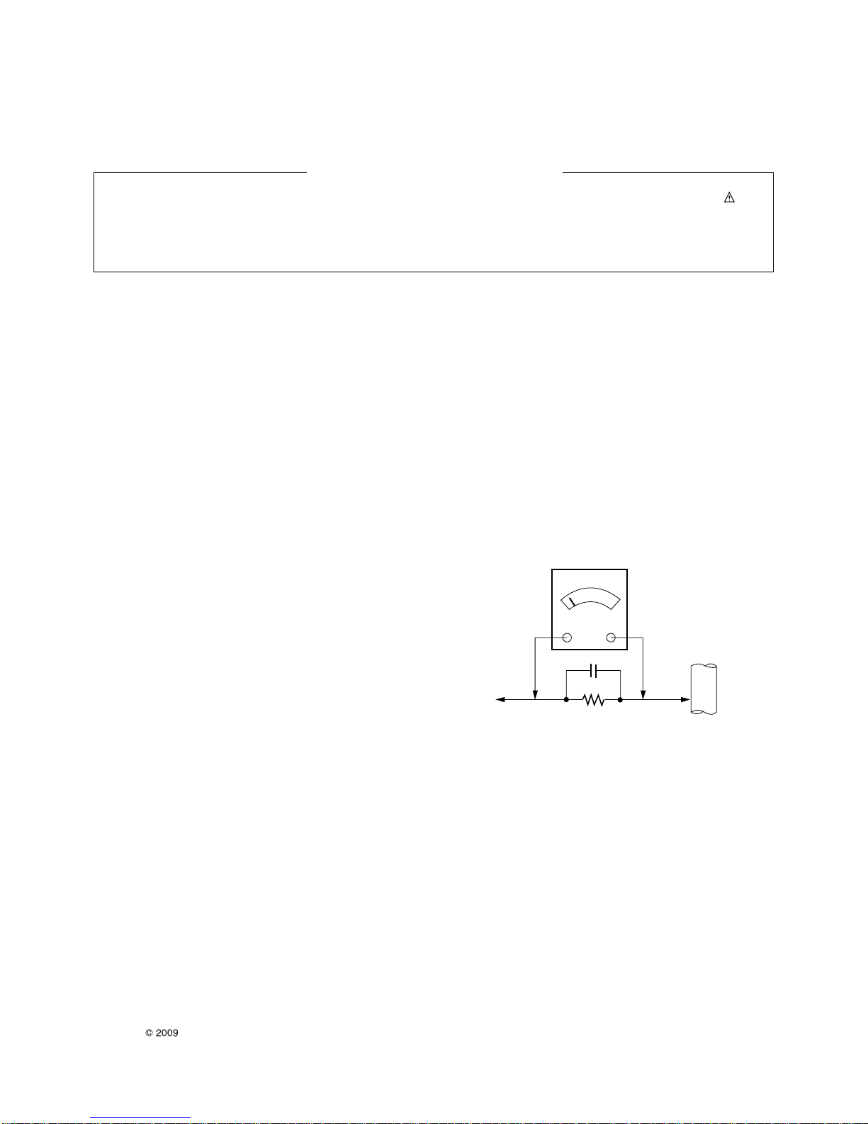
2. Test high voltage only by measuring it with an appropriate high
voltage meter or other voltage measuring device (DVM,
FETVOM, etc) equipped with a suitable high voltage probe.
Do not test high voltage by "drawing an arc".
3. Do not spray chemicals on or near this receiver or any of its
assemblies.
4. Unless specified otherwise in this service manual, clean
electrical contacts only by applying the following mixture to the
contacts with a pipe cleaner, cotton-tipped stick or comparable
non-abrasive applicator; 10% (by volume) Acetone and 90% (by
volume) isopropyl alcohol (90%-99% strength)
CAUTION: This is a flammable mixture.
Unless specified otherwise in this service manual, lubrication of
contacts in not required.
5. Do not defeat any plug/socket B+ voltage interlocks with which
receivers covered by this service manual might be equipped.
6. Do not apply AC power to this instrument and/or any of its
electrical assemblies unless all solid-state device heat sinks are
correctly installed.
7. Always connect the test receiver ground lead to the receiver
chassis ground before connecting the test receiver positive
lead.
Always remove the test receiver ground lead last.
8. Use with this receiver only the test fixtures specified in this
service manual.
CAUTION: Do not connect the test fixture ground strap to any
heat sink in this receiver.
Electrostatically Sensitive (ES) Devices
Some semiconductor (solid-state) devices can be damaged easily
by static electricity. Such components commonly are called
Electrostatically Sensitive (ES) Devices. Examples of typical ES
devices are integrated circuits and some field-effect transistors and
semiconductor "chip" components. The following techniques
should be used to help reduce the incidence of component
damage caused by static by static electricity.
1. Immediately before handling any semiconductor component or
semiconductor-equipped assembly, drain off any electrostatic
charge on your body by touching a known earth ground.
Alternatively, obtain and wear a commercially available
discharging wrist strap device, which should be removed to
prevent potential shock reasons prior to applying power to the
unit under test.
2. After removing an electrical assembly equipped with ES
devices, place the assembly on a conductive surface such as
aluminum foil, to prevent electrostatic charge buildup or
exposure of the assembly.
3. Use only a grounded-tip soldering iron to solder or unsolder ES
devices.
4. Use only an anti-static type solder removal device. Some solder
removal devices not classified as "anti-static" can generate
electrical charges sufficient to damage ES devices.
5. Do not use freon-propelled chemicals. These can generate
electrical charges sufficient to damage ES devices.
6. Do not remove a replacement ES device from its protective
package until immediately before you are ready to install it.
(Most replacement ES devices are packaged with leads
electrically shorted together by conductive foam, aluminum foil
or comparable conductive material).
7. Immediately before removing the protective material from the
leads of a replacement ES device, touch the protective material
to the chassis or circuit assembly into which the device will be
installed.
CAUTION: Be sure no power is applied to the chassis or circuit,
and observe all other safety precautions.
8. Minimize bodily motions when handling unpackaged
replacement ES devices. (Otherwise harmless motion such as
the brushing together of your clothes fabric or the lifting of your
foot from a carpeted floor can generate static electricity
sufficient to damage an ES device.)
General Soldering Guidelines
1. Use a grounded-tip, low-wattage soldering iron and appropriate
tip size and shape that will maintain tip temperature within the
range or 500°F to 600°F.
2. Use an appropriate gauge of RMA resin-core solder composed
of 60 parts tin/40 parts lead.
3. Keep the soldering iron tip clean and well tinned.
4. Thoroughly clean the surfaces to be soldered. Use a mall wire-
bristle (0.5 inch, or 1.25cm) brush with a metal handle.
Do not use freon-propelled spray-on cleaners.
5. Use the following unsoldering technique
a. Allow the soldering iron tip to reach normal temperature.
(500°F to 600°F)
b. Heat the component lead until the solder melts.
c. Quickly draw the melted solder with an anti-static, suction-
type solder removal device or with solder braid.
CAUTION: Work quickly to avoid overheating the circuit
board printed foil.
6. Use the following soldering technique.
a. Allow the soldering iron tip to reach a normal temperature
(500°F to 600°F)
b. First, hold the soldering iron tip and solder the strand against
the component lead until the solder melts.
c. Quickly move the soldering iron tip to the junction of the
component lead and the printed circuit foil, and hold it there
only until the solder flows onto and around both the
component lead and the foil.
CAUTION: Work quickly to avoid overheating the circuit
board printed foil.
d. Closely inspect the solder area and remove any excess or
splashed solder with a small wire-bristle brush.
SERVICING PRECAUTIONS

Copyright LG Electronics. Inc. All right reserved.
Only for training and service purposes - 5 - LGE Internal Use Only
IC Remove/Replacement
Some chassis circuit boards have slotted holes (oblong) through
which the IC leads are inserted and then bent flat against the
circuit foil. When holes are the slotted type, the following technique
should be used to remove and replace the IC. When working with
boards using the familiar round hole, use the standard technique
as outlined in paragraphs 5 and 6 above.
Removal
1. Desolder and straighten each IC lead in one operation by gently
prying up on the lead with the soldering iron tip as the solder
melts.
2. Draw away the melted solder with an anti-static suction-type
solder removal device (or with solder braid) before removing the
IC.
Replacement
1. Carefully insert the replacement IC in the circuit board.
2. Carefully bend each IC lead against the circuit foil pad and
solder it.
3. Clean the soldered areas with a small wire-bristle brush.
(It is not necessary to reapply acrylic coating to the areas).
"Small-Signal" Discrete Transistor
Removal/Replacement
1. Remove the defective transistor by clipping its leads as close as
possible to the component body.
2. Bend into a "U" shape the end of each of three leads remaining
on the circuit board.
3. Bend into a "U" shape the replacement transistor leads.
4. Connect the replacement transistor leads to the corresponding
leads extending from the circuit board and crimp the "U" with
long nose pliers to insure metal to metal contact then solder
each connection.
Power Output, Transistor Device
Removal/Replacement
1. Heat and remove all solder from around the transistor leads.
2. Remove the heat sink mounting screw (if so equipped).
3. Carefully remove the transistor from the heat sink of the circuit
board.
4. Insert new transistor in the circuit board.
5. Solder each transistor lead, and clip off excess lead.
6. Replace heat sink.
Diode Removal/Replacement
1. Remove defective diode by clipping its leads as close as
possible to diode body.
2. Bend the two remaining leads perpendicular y to the circuit
board.
3. Observing diode polarity, wrap each lead of the new diode
around the corresponding lead on the circuit board.
4. Securely crimp each connection and solder it.
5. Inspect (on the circuit board copper side) the solder joints of
the two "original" leads. If they are not shiny, reheat them and if
necessary, apply additional solder.
Fuse and Conventional Resistor
Removal/Replacement
1. Clip each fuse or resistor lead at top of the circuit board hollow
stake.
2. Securely crimp the leads of replacement component around
notch at stake top.
3. Solder the connections.
CAUTION: Maintain original spacing between the replaced
component and adjacent components and the circuit board to
prevent excessive component temperatures.
Circuit Board Foil Repair
Excessive heat applied to the copper foil of any printed circuit
board will weaken the adhesive that bonds the foil to the circuit
board causing the foil to separate from or "lift-off" the board. The
following guidelines and procedures should be followed whenever
this condition is encountered.
At IC Connections
To repair a defective copper pattern at IC connections use the
following procedure to install a jumper wire on the copper pattern
side of the circuit board. (Use this technique only on IC
connections).
1. Carefully remove the damaged copper pattern with a sharp
knife. (Remove only as much copper as absolutely necessary).
2. carefully scratch away the solder resist and acrylic coating (if
used) from the end of the remaining copper pattern.
3. Bend a small "U" in one end of a small gauge jumper wire and
carefully crimp it around the IC pin. Solder the IC connection.
4. Route the jumper wire along the path of the out-away copper
pattern and let it overlap the previously scraped end of the good
copper pattern. Solder the overlapped area and clip off any
excess jumper wire.
At Other Connections
Use the following technique to repair the defective copper pattern
at connections other than IC Pins. This technique involves the
installation of a jumper wire on the component side of the circuit
board.
1. Remove the defective copper pattern with a sharp knife.
Remove at least 1/4 inch of copper, to ensure that a hazardous
condition will not exist if the jumper wire opens.
2. Trace along the copper pattern from both sides of the pattern
break and locate the nearest component that is directly
connected to the affected copper pattern.
3. Connect insulated 20-gauge jumper wire from the lead of the
nearest component on one side of the pattern break to the lead
of the nearest component on the other side.
Carefully crimp and solder the connections.
CAUTION: Be sure the insulated jumper wire is dressed so the
it does not touch components or sharp edges.

Copyright LG Electronics. Inc. All right reserved.
Only for training and service purposes LGE Internal Use Only
- 6 -
4. General Specification(TV)
1. Application Range
This specification sheet is applied to the LCD TV used LA92F
chassis.
2. Specification
Each part is tested as below without special appointment
1) Temperature : 25 ± 5°C (77 ± 9ºF), CST : 40 ± 5ºC
2) Relative Humidity : 65 ±10%
3) Power Voltage : Standard input voltage
(100-240V@ 50/60Hz)
* Standard Voltage of each products is marked by models
4) Specification and performance of each parts are followed
each drawing and specification by part number in
accordance with BOM.
5) The receiver must be operated for about 20 minutes prior to
the adjustment.
3. Test method
1) Performance : LGE TV test method followed.
2) Demanded other specification
- Safety : UL, CSA, IEC specification
- EMC : FCC, ICE, IEC specification
SPECIFICATION
NOTE : Specifications and others are subject to change without notice for improvement
.
No Item Specification Remark
1. Receiving System 1) ATSC / NTSC-M
2. Available Channel 1) VHF : 02~13
2) UHF : 14~69
3) DTV : 02-69
4) CATV : 01~135
5) CADTV : 01~135
3. Input Voltage 1) AC 100 ~ 240V 50/60Hz Mark : 110V, 60Hz (N.America)
Mark : 220V,60Hz (Korea)
4. Market NORTH AMERICA
KOREA
LH85-UC
LH80YD-NB
42 inch Wide(1920 ◊1080) FHD + 120Hz 42LH80YD-NB
47 inch Wide(1920 ◊1080) FHD + 120Hz 47LH85-UC / 47LH80YD-NB
5. Screen Size
55 inch Wide(1920 ◊1080) FHD + 120Hz 55LH85-UC / 55LH80YD-NB
6. Aspect Ratio 16:9
7. Tuning System FS
LC420WUF-SBB1 (without inverter) LGD 42LH80YD-NB
LC470WUF-SBB1 (without inverter) LGD 47LH85-UC / 47LH80YD-NB
8. Module
LC550WUD-SBA1 LGD 55LH85-UC / 55LH80YD-NB
9. Operating Environment 1) Temp : 0 ~ 40 deg
2) Humidity : ~ 80 %
10. Storage Environment 1) Temp : -20 ~ 60 deg
2) Humidity : ~ 85 %

Copyright LG Electronics. Inc. All right reserved.
Only for training and service purposes LGE Internal Use Only
- 7 -
5. Chroma & Brightness
No Item Min Typ Max Unit Remark
400 500 cd/m 42LH80YD-NB
400 500 cd/m 47LH85-UC / 47LH80YD-NB
1. Max Luminance
(Center 1-point / Full White Pattern) 400 500 cd/m 55LH85-UC / 55LH80YD-NB
2.
3. Luminance uniformity 77 % Full white
0.636
4. RED 0.334
5. 0.290
6. GREEN 0.608
7. 0.145
8. BLUE 0.064
9. 0.279
10. WHITE
Y
X
Y
X
Y
X
Y
X
Y
X
Y
X
Y
X
Y
X
Y
X
Y
X
Y
X
Y
X
Typ.
-0.03
0.292
Typ.
+0.03 47LH85-UC / 47LH80YD-NB
11. 0.637
12. RED 0.333
13. 0.287
14. GREEN 0.605
15. 0.145
16. BLUE 0.064
17. 0.279
18. WHITE
Typ.
-0.03
0.292
Typ.
+0.03 55LH85-UC / 55LH80YD-NB
19. 0.638
20. RED 0.334
21. 0.290
22. GREEN 0.606
23. 0.144
24. BLUE 0.064
25. 0.279
26.
Color
coordinate
WHITE
Typ.
-0.03
0.292
Typ.
+0.03 42LH80YD-NB
27. Color coordinate uniformity N/A
1000:1
8000:1 1400:1
10000:! 42LH80YD-NB
DCR
28. Contrast ratio
1000:1
8000:1 1400:1
10000:! 47LH85-UC / 47LH80YD-NB
DCR
1000:1
8000:1 1400:1
10000:1 55LH85-UC / 55LH80YD-NB
DCR
Cool 0.274
0.281 0.276
0.283 0.278
0.285 11000K
Medium 0.283
0.291 0.285
0.293 0.287
0.295 9300K
29. Color
Temperature
Warm 0.311
0.327 0.313
0.329 0.315
0.331 6500K
** W/B 편차는 화질 향상을
위해 DQA ±0.015로 관리
(The W/B Tolerance is
–0.015 for Adjustment)
30. Color Distortion, DG 10.0 %
31. Color Distortion, DP 10.0 deg
32. Color S/N, AM/FM 43.0 dB
33. Color Killer Sensitivity -80 dBm

Copyright LG Electronics. Inc. All right reserved.
Only for training and service purposes LGE Internal Use Only
- 8 -
7. RGB input (PC)
6. Component Video Input (Y, CB/PB, CR/PR)
No Resolution H-freq(kHz) V-freq.(Hz) Pixel clock Proposed
1. 720*480 15.73 60 13.5135 SDTV ,DVD 480I
2. 720*480 15.73 59.94 13.5 SDTV ,DVD 480I
3. 720*480 31.50 60 27.027 SDTV 480P
4. 720*480 31.47 59.94 27.0 SDTV 480P
5. 1280*720 45.00 60.00 74.25 HDTV 720P
6. 1280*720 44.96 59.94 74.176 HDTV 720P
7. 1920*1080 33.75 60.00 74.25 HDTV 1080I
8. 1920*1080 33.72 59.94 74.176 HDTV 1080I
9. 1920*1080 67.500 60 148.50 HDTV 1080P
10. 1920*1080 67.432 59.94 148.352 HDTV 1080P
11. 1920*1080 27.000 24.000 74.25 HDTV 1080P
12. 1920*1080 26.97 23.976 74.176 HDTV 1080P
13. 1920*1080 33.75 30.000 74.25 HDTV 1080P
14. 1920*1080 33.71 29.97 74.176 HDTV 1080P
No Resolution H-freq(kHz) V-freq.(Hz) Pixel clock(MHz) Proposed
PC DDC
1. 640*350 31.468 70.09 25.17 EGA
2. 720*400 31.469 70.08 28.32 DOS O
O
3. 640*480 31.469 59.94 25.17 VESA(VGA) O
4. 800*600 37.879 60.31 40.00 VESA(SVGA) O
5. 1024*768 48.363 60.00 65.00 VESA(XGA) O
O
O
6. 1280*768 47.776 59.870 79.5 CVT(WXGA)
7. 1360*768 47.712 60.015 85.50 VESA (WXGA)
8. 1280*1024 63.981 60.020 108.00 VESA (SXGA) O
9. 1600*1200 75.00 60.00 162 VESA (UXGA) O
10 1920*1080 66.587 59.934 148.5 HDTV 1080P O

- 9 - LGE Internal Use OnlyCopyright LG Electronics. Inc. All right reserved.
Only for training and service purposes
9. Mechanical Specification
1) Media Box
No Item CONTENT Unit REMARK
1 Protrusion TBD
2 Appearance
quality Satisfy appearance inspection LG(56)-G3-1002
Before Packing 426(W) X 234.5(D) X 68.6(H) mm
3 Product
Dimension After Packing 432(W) X 249(D) X 76(H) mm
Media-Box ONLY 2.6 Kg
4 Product
Weight With BOX 3.1 Kg
GAP
단차
단차
mm
TOP COVER & BOTTOM Measure(DQA)
SPEC
SPEC
1mm mm
TOP COVER & BOTTOM Measure(DQA)
SPEC
SPEC
SPEC
1mm mm
REAR SHIELD & BOTTOM SHIELD Measure(DQA)
GAP MAX 1mm mm
BOTTOM COVER & REAR SHIELD Measure(DQA)
Measure(DQA)
GAP MAX
MAX
1mm
MAX
MAX
1.2mm mm
5 Test SPEC
TOP COVER & REAR SHIELD
8. HDMI input (PC/DTV)
No Resolution H-freq(kHz) V-freq.(Hz) Pixel clock(MHz) Proposed
PC DDC
1. 640*350 31.468 70.09 25.17 EGA
2. 720*400 31.469 70.08 28.32 DOS O
O
3. 640*480 31.469 59.94 25.17 VESA(VGA) O
4. 800*600 37.879 60.31 40.00 VESA(SVGA) O
5. 1024*768 48.363 60.00 65.00 VESA(XGA) O
O
6. 1280*768 47.776 59.870 79.5 CVT(WXGA)
7. 1360*768 47.712 60.015 85.50 VESA (WXGA) O
8. 1280*1024 63.981 60.020 108.00 VESA (SXGA) O
9. 1600*1200 75.00 60.00 162 VESA (UXGA) O
10. 1920*1080 67.5 60 148.5 HDTV 1080P O
DTV
1 720*480 31.47 60 27.027 SDTV 480P
2 720*480 31.47 59.94 27.00 SDTV 480P
3 1280*720 45.00 60.00 74.25 HDTV 720P
4 1280*720 44.96 59.94 74.176 HDTV 720P
5 1920*1080 33.75 60.00 74.25 HDTV 1080I
6 1920*1080 33.72 59.94 74.176 HDTV 1080I
7 1920*1080 67.500 60 148.50 HDTV 1080P
8 1920*1080 67.432 59.939 148.352 HDTV 1080P
9 1920*1080 27.000 24.000 74.25 HDTV 1080P
10 1920*1080 26.97 23.976 74.176 HDTV 1080P
11 1920*1080 33.75 30.000 74.25 HDTV 1080P
12 1920*1080 33.71 29.97 74.176 HDTV 1080P

- 10 - LGE Internal Use OnlyCopyright LG Electronics. Inc. All right reserved.
Only for training and service purposes
2) 55LH85-UC
NO ITEM CONTENT UNIT REMARK
Width Height
1373 964.3 mm With Stand
W/O Packing 1373 888.5 mm W/O Stand
1485 1063 mm With Stand
1 Product
Dimension With Packing 1485
Depth
454.2
106.9
570
355 1012 mm W/O Stand
39.2 Kg With Stand
W/O Packing
(CCFL Module) 33.8 Kg W/O Stand
40.9 Kg With Stand
W/O Packing
(LED Module) 35.5 Kg W/O Stand
44.9 Kg With Stand
With Packing
(CCFL Module) 39.5 Kg W/O Stand
46.6 Kg With Stand
2 Product
Weight
With Packing
(LED Module) 41.2 Kg W/O Stand
64 With Stand
40ft
(Normal) 96
64
96
–20¡
W/O Stand
With Stand
3 Container
Loading
Quantity Individual 40ft
(H-Cubic)
Set
Set
Set
Set
Swivel YES/NO
YES/NO
Angle Degree
Tilt
Funchion
Angle Front( )/Back( ) Degree
Width Height
572 Depth
454.2 276.2 mm With Neck
Dimension
(W/O Packing) -- --
----
--
--
--
-- 5.4
-- --
--
mm W/O Neck
Dimension(With Packing) mm Commercial
Weight(W/O Packing) Kg With Neck
4 Stand Assy
Weight(With Packing) Spec 2.0(1.5~3.0) Kgf Set
5 Test Spec Swivel Force Measure
(DQA) Kgf Set
Spec 0.2¡/-1.3¡ Degree
Degree
Set
Inclination
(Front/Back) Measure
(DQA) --
--
Set
Spec sec
sec
Set
Wobble Measure
(DQA) Set
Spec mm
mm
Set
Difference
(Left/Right) Measure
(DQA) -- Set
GAP(C/A & Module) Spec Max 1.0 mm
mm
Set
Measure
(DQA) -- Set
GAP(C/A & B/C) Spec Max 1.2 (delt
Max 15sec
Max 5mm
a 1.0) mm
mm
mm
Set
Measure
(DQA) Set
GAP(B/C & Control) Spec Max 0.8 mm Set
Measure
(DQA) Set
GAP(B/C & Side AV) Spec Max 0.8 mm
mm
mm
Set
Measure
(DQA) Set
SIDE GAP(C/A & B/C ) Spec Max 1.3 (delta 0.7) mm
Measure
(DQA) Set
6 Appearance Refer to Standard of LG(56)G4-9002

Copyright LG Electronics. Inc. All right reserved.
Only for training and service purposes
1. Application Object
This specification sheet applied to LA92F Chassis applied
LCD TV all models manufactured in TV factory.
2. Notes
1) Because this is not a hot chassis, it is not necessary to use
an isolation transformer. However, the use of isolation
transformer will help protect test instrument.
2) Adjustment must be done in the correct order. But it is
flexible when its factory local problem occurs. .
3) The adjustment must be performed in the circumstance of
25 ±5°C of temperature and 65±10% of relative humidity if
there is no specific designation.
4) The input voltage of the receiver must keep 220V, 60Hz.
5) Before adjustment, execute Heat-Run for 5 minutes.
•How to make set white pattern
1) Press Power ON button of Service Remocon
2) Press ADJ button of Service remocon. Select “7. Test
pattern”and, after select “White”using navigation button,
and then you can see 100% Full White pattern.
* In this status you can maintain Heat-Run useless any
pattern generator
* Notice: if you maintain one picture over 20 minutes
(Especially sharp distinction black with white pattern –
13Ch, or Cross hatch pattern –09Ch) then it can appear
image stick near black level.
3. Adjustment items
3.1. Board adjustment
- ADC Calibration(Media-Box Only)
- EDID/DDC download
Above adjustment items can be also performed in Final
Assembly if needed. Both Board-level and Final assembly
adjustment items can be check using In-Star Menu 1.ADJUST
CHECK.
* Don't use Instop key after Media-Box Main b/d board test
and Media-Box assemble & test.
3.2. Final assembly adjustment
- Wireless Pairing
- White Balance adjustment
- RS-232C functionality check
- Factory Option setting per destination
- EYE-Q Test
- Ship-out mode setting (In-Stop)
3.3 Etc
- Ship-out mode
- Service Option Default
4. Automatic Adjustment
4.1. ADC(LGE3369) Adjustment
4.1.1 Overview
ADC adjustment is needed to find the optimum black level
and gain in Analog-to-Digital device and to compensate
RGB deviation.
4.1.2 Equipment & Condition
1) Jig (RS-232C protocol)
2) External/Internal Pattern
- ADC Comp 480i / ADC Comp 1080p
=> Select component 480i signal that is same as the
image below on the Media-Box with using Pattern
Generator(MSPG-925FA or etc)
3) Adjustment ADC RGB
=> Using Internal Pattern
4) Image
4.1.3 Adjustment
4.1.3.1 Adjustment method
- Using RS-232, adjust items listed in 3.1 in the other
shown in “4.1.3.3”
4.1.3.2 Adj. protocol
Ref.) ADC Adj. RS232C Protocol_Ver1.0
4.1.3.3 Adj. order
- aa 00 00 [Enter ADC adj. mode]
- xb 00 04 [Change input source to Component1]
- ad 00 10 [Adjust 480i Comp1]
- xb 00 60 [Change input source to RGB-DTV]
- ad 00 10 [Adjust 1080p Comp1/RGB]
- ad 00 90 End adj.
LGE Internal Use Only
- 11 -
ADJUSTMENT INSTRUCTION
Protocol Command Set ACK
Enter adj. mode aa 00 00 a 00 OK00x
Source change xb 00 40 b 00 OK40x (Adjust 480i Comp1 )
xb 00 60 b 00 OK60x (Adjust 1024*768 RGB)
Begin adj. ad 00 10
Return adj. result OKx (Case of Success)
NGx (Case of Fail)
Read adj. data (main) (main)
ad 00 20 000000000000000000000000007c007b006dx
(sub) (Sub)
ad 00 21 000000070000000000000000007c00830077x
Confirm adj. ad 00 99 NG 03 00x (Fail)
NG 03 01x (Fail)
NG 03 02x (Fail)
OK 03 03x (Success)
End adj. aa 00 90 a 00 OK90x

4.2. EDID(The Extended Display Identification
Data)/DDC(Display Data Channel) download
4.2.1 Overview
It is a VESA regulation. PC or a MNT will display an
optimal resolution through information sharing without any
necessity of user input. It is a realization of “Plug and Play”.
4.2.2 Equipment
- Adjust remocon
4.2.3 Download method
1) Press ADJ key on the adjustment R/C and select [EZ
ADJUST]. Select [8.EDID D/L] and access to the items
with using the ENTER key.
2) Press the OK key on the [Start] menu, HDMI1 / HDMI2 /
HDMI3 / HDMI4 / RBG inputs are selected on the
Media-Box and HDMI5 input on the TV. When the
process is completed, the message 'NG' is changed to
'OK'.
* You can download this with using JIG or the equipment
on the HDMI5 / RGB input.
4.2.4 EDID DATA
- HDMI
EDID Block 0 table =
EDID Block 1 table =
* Notice
- HDMI1 ~ HDMI4 / RGB : Media-Box, Hdmi5 : TV
-The items below of the EDID datas can be changed
according to the S/W and input.
=> VV:Week Manufacture
=> WW: Year Manufacture
=> XX:C/S
=> YY : Physical address
5. Total Assembly Adjustment
•The Wireless model can be added the pairing work with the
Media-Box besides the existing test and can be changed
the process and the test method.
•Total Assembly process
- TV Tool option check
- Connect the TV and Media-Box wireld with the HDMI
cable. (TV: HDMI5 port / Media-Box: Service port)
- Wireless Pairing
- Media-Box Tool option check
- Media-Box AC power off
- Remove the HDMI cable
- Adjust the White Balance
- Media-Box AC power on (Access to Wireless mode)
- Check the Display and press the Bluetooth key (send the
TV W/B data to Media-Box)
- Connect the RF / HDMI1 to Media-Box and check.
- Shipping
* The Media-Box is the main equipment and the TV is after on
the Wireless/Wired connection and the Media-Box can
adjust all of the OSD)
(exception: Select the HDMI5 on the Wireless connection)
5.1 Wireless Pairing
5.1.1 Overview
To set 1:1 connection from selecting the same Wireless
channel on the TV and Media-Box, and fixing Mac
address.
* Set this on the Wired (HDMI cable connection) state.
5.1.2 Method
1) Press one of the OP1(Channel1) / OP2(Channel2) /
OP3(Channel3) key on the adjustment R/C and check
the Paring information OSD that is displayed
2) Use these method if the upper method can not be
processed
- 12 - LGE Internal Use OnlyCopyright LG Electronics. Inc. All right reserved.
Only for training and service purposes

5.2. White Balance Adjustment
5.2.1 Overview
•W/B adj. Objective & How-it-works
- Objective: To reduce each Panel’s W/B deviation
- How-it-works: When R/G/B gain in the OSD is at 192, it
means the panel is at its Full Dynamic
Range. In order to prevent saturation of
Full Dynamic range and data, one of
R/G/B is fixed at 192, and the other two is
lowered to find the desired value.
5.2.2 Equipment
1) Color Analyzer: CA-210 (NCG: CH 9 / WCG: CH12)
2) Adj. Computer(During auto adj., RS-232C protocol is
needed)
3) Adjust Remocon
4) Video Signal Generator MSPG-925F 720p/216-Gray
(Model:217, Pattern:78)
-> Only when internal pattern is not available
•Color Analyzer Matrix should be calibrated using CS-1000
5.2.3 Equipment connection
5.2.4 Adj. Command (Protocol)
- LEN : Number of Data Byte
- CMD : Command
- VAL : Value of FOS Data
- CS : Checksum
- A : Acknowledge
Ex) [Send: JA_00_DD] / [Ack: A_00_okDDX}
•
RS-232C Command(Automatic adjustment)
Ex) wb 00 00 : Start Auto-adjustment of white balance.
wb 00 10 : Start Gain Adjustment (Inner pattern)
ja 00 ff : Adjustment data
jb 00 c0 :
…
…
wb 00 1f : End of Gain adjustment
* (wb 00 20(start), wb 00 2f(end)) -> In the case of Off-
set adjustment
wb 00 ff : End of white balance adjustment
•
Adjustment Map
- 13 - LGE Internal Use OnlyCopyright LG Electronics. Inc. All right reserved.
Only for training and service purposes
Color Analyzer
Computer
Pattern Generator
RS-232C
RS-232C
RS-232C
Probe
Signal Source
* If TV internal pattern is used, not needed
Connection Diagram of Automatic Adjustment
START 6E 50 03 00 CSLEN CMD VAL STOPA A A A A A A A
RS-232C COMMAND Meaning
[CMD ID DATA]
wb 00 00 White Balance adjustment start.
wb 00 10 Start of adjust gain (Inner white pattern)
wb 00 1f End of gain adjust
wb 00 20 Start of offset adjust(Inner white pattern)
wb 00 2f End of offset adjust
wb 00 ff
End of White Balance adjust(Inner pattern disappeared)
ITEM Command Data Range Default
(Hex.) (Decimal)
Cmd 1 Cmd 2 Min Max
Cool R-Gain j g 00 C0 TBD
G-Gain j h 00 C0 TBD
B-Gain j i 00 C0 TBD
R-Cut TBD
G-Cut TBD
B-Cut TBD
Medium R-Gain j a 00 C0 TBD
G-Gain j b 00 C0 TBD
B-Gain j c 00 C0 TBD
R-Cut TBD
G-Cut TBD
B-Cut TBD
Warm R-Gain j d 00 C0 TBD
G-Gain j e 00 C0 TBD
B-Gain j f 00 C0 TBD
R-Cut TBD
G-Cut TBD

Copyright LG Electronics. Inc. All right reserved.
Only for training and service purposes
5-3. Adjustment of White Balance
5.3.1 Automatic Adjustment
1) The adjustment condition should be set by the Power On
key.
2) Perform the zero calibration of the Color Analyzer and
place the probe close to the display center.
3) Connect the communication cable (RS-232C).
4) Select the desired model of the adjustment program and
perform the adjustment.
5) After the adjustment is ended (check the OK sign), check
the adjustment condition for each mode of the set.
(Warm, Medium, Cool)
6) Disconnect the probe and the communication cable to end
the adjustment.
* The adjustment should be started with "wb 00 00" and
ended with "wb 00 ff", and the offset should be adjusted
when necessary.
5.3.2 Manual adj. method
1) Set TV in Adj. mode using POWER ON
2) Press the ADJ of the R/C to enter into ‘EZ-ADJUST’.
3) Select ‘10.TEST PATTERN’with the CH +/- key and press
the Enter key for 30 minutes or longer to perform the heat
run.
4) Perform the zero calibration of the Color Analyzer and fix
the sensor with the 10cm or less distance at the center of
the LCD module surface when adjusting.
5) Press the ADJ of the R/C to select ‘7.White-Balance’of the
Ez-Adjust and press the right arrow key(G) to enter into the
adjustment mode. (As soon as you press ‘G’, the screen is
entered into the full white inner pattern.)
6) Fix one of the R/G/B gains to 192 and decrease the
remaining two gains to adjust not to exceed 192.
7) The adjustment is done at three white balances of Cool,
Medium and Warm
* Adjustment environment and reference
1) Environment illuminance
Adjust it to 10 LUX or less at the place where the light
source such as lamp should be blocked at maximum.
2) Probe location
: Maintain the Color Analyzer (CA-210) close to the
module surface by 10cm or less and keep the probe of
the Color Analyzer perpendicular to the module
surface (80°~ 100°).
3) Aging time
- Keep the power on after the aging start (with no power
off) to perform the heat run for 15 minutes or longer.
- Make sure that the back light is turned on by using no
signal and the full white pattern or others.
•Standard color coordinate and temperature using CS-
1000 (over 26 inch)
•Standard color coordinate and temperature using CA-
210(CH 9)
5.4 Option selection per country
(1) Overview
- Option selection is only done for models in Non-USA
North America due to rating
-Applied model: LA92A Chassis applied None USA
model(CANADA, MEXICO)
(2) Method
1) Press ADJ key on the Adj. R/C, then select Country
Group Menu
2) Depending on destination, select KR or US, then on the
lower Country option, select US, CA, MX. Selection is
done using +, - KEY
•TV
- Adjust directly if it's not a Wireless/Wired state
- Adjust after changing to HDMI5 on the Wireless/Wired state
•Media-Box
- Adjust on the Wireless/Wired state that is excepted the
HDMI5.
LGE Internal Use Only
- 14 -
Mode Color Coordination Temp ∆UV
xy
COOL 0.276 0.283 11000K 0.0000
MEDIUM 0.285 0.293 9300K 0.0000
WARM 0.313 0.329 6500K 0.0000
Mode Color Coordination Temp ∆UV
xy
COOL 0.276±0.002 0.283±0.002 11000K 0.0000
MEDIUM 0.285±0.002 0.293±0.002 9300K 0.0000
WARM 0.313+0.002 0.329±0.002 6500K 0.0000

Copyright LG Electronics. Inc. All right reserved.
Only for training and service purposes LGE Internal Use Only
- 15 -
6. EYE-Q function check
Step 1) Turn on TV
Step 2) Press EYE key of Adj. R/C
Step 3) Cover the Eye Q II sensor on the front of the using
your hand and wait for 6 seconds
Step 4) Confirm that R/G/B value is lower than 10 of the
“Raw Data (R: G: B: )”.
If after 6 seconds, R/G/B value is not lower than 10,
replace Eye Q II sensor
Step 5) Remove your hand from the Eye Q II sensor and wait
for 6 seconds
Step 6) Confirm that “B. Light(xxx)”value increases from 0.
If change is not seen, replace Eye Q II sensor
< step 2> < step 3> < step 4>
< step 5> < step 6>
7. GND and Internal Pressure check
7.1 Method
1) GND & Internal Pressure auto-check preparation
- Check that Power Cord is fully inserted to the set
(If loose, re-insert)
2) Perform GND & Internal Pressure auto-check
- Unit w/ fully inserted power cord and A/V arrives to the auto-
check process.
- Connect D-terminal AV JACK TESTER
- Auto CONTROLLER(GWS103-4) ON
- Perform GND TEST
- If NG, Buzzer will sound to inform the operator
- If OK, changeover to I/P check automatically
(Remove CORD,A/V from AV Jack Box)
- Perform I/P test
- If NG, Buzzer will sound to inform the operator
- If OK, Good lamp will lit up and the stopper will allow the
pallet to move on to next process.
7.2 Checkpoint
•TEST voltage
- GND: 1.5KV/min at 100mA
- Signal: 3KV/min at 100mA
•Test time: 1 second
•Test point
- GND test = Power cord GND & signal cable metal GND
- Internal pressure TEST = POWER CORD GND & LIVE &
NEUTRAL
•LEAKAGE CURRENT: At 0.5mArms
Green Eye-Check
Sensor Data: 1
Backlight: 0
O.K
Green Eye-Check
SensorData: 215
Backlight : 100

Copyright LG Electronics. Inc. All right reserved.
Only for training and service purposes - 16 - LGE Internal Use Only
EXPLODED VIEW
300
200T
200
200N
121
570
120 510
500
560
810
800
805
540
804
803
530
801
806 550
820
910
900
520
820
400
802
310
700
710
770
780
790
720
730
750
740
760
A2
LV1
A10
LV2
Many electrical and mechanical parts in this chassis have special safety-related characteristics. These
parts are identified by in the Schematic Diagram and EXPLODED VIEW.
It is essential that these special safety parts should be replaced with the same components as
recommended in this manual to prevent X-RADIATION, Shock, Fire, or other Hazards.
Do not modify the original design without permission of manufacturer.
IMPORTANT SAFETY NOTICE
Media Box

USB DOWN STREAM
THE SYMBOL MARK OF THIS SCHEMETIC DIAGRAM INCORPORATES
SPECIAL FEATURES IMPORTANT FOR PROTECTION FROM X-RADIATION.
FILRE AND ELECTRICAL SHOCK HAZARDS, WHEN SERVICING IF IS
ESSENTIAL THAT ONLY MANUFATURES SPECFIED PARTS BE USED FOR
THE CRITICAL COMPONENTS IN THE SYMBOL MARK OF THE SCHEMETIC.
IN/OUT
JK502
KCN-DS-1-0088
6630G00001C
1
2
3
4
5
6
7
8
9
10
+3.3V_ST
L502
BLM18PG121SN1D
R510 100
R509 100
IC500
MAX3232CDR
EAN41348201
3
C1-
2
V+
4
C2+
1
C1+
6
V-
5
C2-
7
DOUT2
8
RIN2 9ROUT2
10 DIN2
11 DIN1
12 ROUT1
13 RIN1
14 DOUT1
15 GND
16 VCC
ISP_RXD
9:AC30;Y26 R522 0
OPT
+5V_Wireless
JK503
UB01123-4HHS-4F
1234
5
L500
CB3216PA501E
USB_PWR_CTL
USB_DM 9:AO37
USB_DP 9:AO37
D502
30V
CDS3C30GTH
OPT
D501
30V
CDS3C30GTH
OPT
+5V_EXT
L505
CB3216PA501E
READY_USB_POWER
FAN_POWER
L503
BLM18PG121SN1D
OPT
FAN_ERROR
9:AO26;12:AF16
P500
TJC2508-4A
ISP_S5
1
2
3
4
ISP_RXD
9:AC30;R25
ISP_TXD
9:AC30;R25
ISP_TXD
9:AC30;Y25 R521 0
OPT
R502
2.2K
+5V
R503
2.2K
R516
4.7K
OPT
+3.3V_ST
R517
4.7K
OPT UART_RXD 9:AC30
UCOM_RXD 12:AF17
RXD_232 AF22
EYE_LED_SDA
9:AT6;12:AF16
L509
BG2012B080TF
R538
0
R537
0
EYE_LED_SCL
9:AT6;12:AF16
IR
12:M15
R534
0
+3.3V
L512
CB3216PA501E
L506
CB3216PA501E
+5V_ST
C524
0.1uF
16V
C527
1000pF
50V
C522
0.1uF
16V C523
1000pF
50V
KEY1
12:W8
ZD501
5.6B
+3.3V_ST
L508
BG2012B080TF
R525
100 1%
R527
4.7K
L507
BG2012B080TF
KEY2
12:W8
R526
100 1%
R530
4.7K
C525
0.1uF
ZD500
5.6B
C526
0.1uF
C517
0.1uF
16V
OPT
D500
CDS3C05HDMI1
OPT
R531
0
OPT
RL_ON
4:O26;4:Q25;12:AF18 R533
4.7K
OPT
Q500
2SC3052
OPT
E
B
C
+3.3V_ST
R535
10K
OPT
D504
30V
CDS3C30GTH
C543
47pF
50V
C542
220pF
50V
D503
30V
CDS3C30GTH C545
47pF
50V
C544
220pF
50V
R542 220
R543 220
C505
0.1uF
C504
0.1uF
C503
0.1uF
C507
0.1uF
C546 0.33uF
D506
5.6V
CDS3C05HDMI1
D507
5.6V
CDS3C05HDMI1
R544
4.7K
OPT
C511
0.1uF
16V
USB_PWR_CTL
R540
180
USB_PWR_CTL USB_CTL
9:AO18
IC506
MIC2009YM6-TR
USB_PWR_CTL
EAN43439401
3ENABLE
2GND
4
FAULT/
1VIN
6
VOUT
5
ILIMIT
+5V_EXT
R541
47
USB_PWR_CTL
R519
10K
USB_PWR_CTL
USB_OCD 9:AO31
+3.3V
C513
10uF
10V
USB_PWR_CTL
R545
120K
OPT
R532
0
LED_ON
12:T8
R539
0
C528
100pF
50V
ZD502
5.6B
+3.3V_ST
L513
22UH
R529
100
READY
C540
0.1uF
16V
C532
0.47uF
25V
FAN_EN
AC4;12:AF15
IC504
MP2305DS
EAN33143501
3
SW
2
IN
4
GND
1
BS
5FB
6COMP
7EN
8SS
R528
10K
1%
L510
CB3216PA501E
READY
R523
56K
1%
C538
0.1uF
16V
C535
0.01uF
50V
C531
10uF
16V
+12V
C537
22uF
16V
C539
0.1uF
50V
FAN_POWERC536
5600pF
50V
R524
9.1K
R515
10K
OPT
R553
2K
OPT
R505
4.7K
Q501
RTR030P02
S
D
G
+5V_ST
L517
BLM18PG121SN1D
OPT
L516
BLM18PG121SN1D
+5V_EXT
Q502
2SC3052
E
B
C
R549
10K
R550
560
C518
0.1uF
R551
10K
OPT
FAN_EN
AM6;12:AF15
RX_EN
O4;12:X25
R552
10K
C520
0.1uF
16V
C519
10uF
16V
C501
330uF
25V
C516
1uF
C549
0.1uF
16V
C547
1uF
R506
100K
C548 820pF
+5V_Wireless
R556
11K
1%
C509
100uF
16V
C554
100uF
16V
OPT
C550 22pF
L514
10uH R513
27K
+12V
IC501
APW7080KAI-TRL
EAN50480501
3
UGND
2
EN
4
VCC
1
VIN
5LX
6COMP
7FB
8GND
C514
22uF
16V
Q504
SI4925BDY
EBK32753101
Protect In-rush current
3S2
2G1
4G2
1S1
5 D2_1
6 D2_2
7 D1_1
8 D1_2
C553
1uF
C551
68pF
C502
47uF
25V
R518
24K
L501
CB3216PA501E
C510
0.1uF
50V
R558
59K
1%
C508
10uF
25V
D505
500MV
MBRS340T3G
C534
100pF
50V
OPT
C533
100pF
50V
OPT
C515
1uF
R514
8.2K
R511
10K
RX_EN
AC3;12:X25
C552
1uF
OPT
Q503
2SC3052
E
B
C
L504
UBW3216-121
P502
12507WS-08L
1
2
3
4
5
6
7
8
9
C512
0.1uF
P501
SMW200-03
1
2
3
R507 0 OPT
R500 0
R508 0
C506
10uF
16V
C500
0.1uF
16V
UART_SEL2
AJ22;12:U25 UART_SEL2
P22;12:U25
+3.3V_ST
C529
0.1uF C521
0.1uF
R501
10K
R555
10K
OPT
RXD_232
L23
IC503
NLASB3157DFT2G
EAN38256201
ANALOG SWITCH
ON SEMICONDUCTOR
OPT
3B0
2GND
4
A
1B1
6
SELECT
5
VCC
RXD_WIRELESS
2:J23
UART_SEL1
12:T25
+3.3V_ST
IC502
NLASB3157DFT2G
EAN38256201
ANALOG SWITCH
ON SEMICONDUCTOR
3
B0
2
GND
4A
1
B1 6SELECT
5VCC
+3.3V_ST
UCOM_TXD
12:AF17
TXD_WIRELESS
9:AO31;2:J22
R512
10K
OPT
RXD_S5
9:AO31
R504 0
UART_TXD
9:AC30
IC505
NLASB3157DFT2G
EAN38256201
ANALOG SWITCH
ON SEMICONDUCTOR
3B0
2GND
4
A
1B1
6
SELECT
5
VCC
C530
0.1uF
OPT
P503
12507WS-12L
1
SCL
2
SDA
3
GND
4
KEY1
5
KEY2
6
ST_5V
7
GND
8
WARM_ST
9
IR
10
GND
11
3.3V
12
LED_ON
13
.
C555
0.1uF
16V
OPT
C541
0.1uF
FOR EMI
1
IN/OUT
JUNO
12
RS232C & ISP
USB
RX B/D FAN
USB POWER CONTROL OPTION
ISP FOR S5
[CONTROL IR & LED]
WIRELESS RX BOARD POWER
Pin to Pin Replacable with T-MIC2019YM6
DO JAE GEUN
09.02.04
Vout=0.923*(R1+R2)/R2
---------------------
R1
R2
READY FOR FAN POWER VOLTAGE CONTROL
R1
R24A/10ms
Vout=0.8*(1+R1/R2)
UART CONNECTION
================================
MICOM S5 RX_B/D
--------------------------------
UART_SEL1: L H X
UART_SEL2: L L H
--------------------------------
S5 <-> RX: CON CON DIS-CON
CONNECT
================================

THE SYMBOL MARK OF THIS SCHEMETIC DIAGRAM INCORPORATES
SPECIAL FEATURES IMPORTANT FOR PROTECTION FROM X-RADIATION.
FILRE AND ELECTRICAL SHOCK HAZARDS, WHEN SERVICING IF IS
ESSENTIAL THAT ONLY MANUFATURES SPECFIED PARTS BE USED FOR
THE CRITICAL COMPONENTS IN THE SYMBOL MARK OF THE SCHEMETIC.
SCL_DDC F11
HDMI0_RX0- 9:F36
C300
0.1uF
50V
R324
100
EEPROM_WP 9:AO25
HDMI1_RX0+ 9:F34
HDMI1_RX2+ 9:F33
R322
10K
HDMI0_RX1+ 9:F36
HDMI1_RX1- 9:F33
+5V
CEC S27
HDMI0_RXC- 9:F36
HDMI1_SCL 9:F32
HDMI1_SDA 9:F33
C304
8pF
50V
OPT
VR305
VR304
AVRL161A1R1NT
10V
HDMI1_POWER 9:V29;D13
HDMI0_RX1- 9:F36
HDMI1_RXC+ 9:F34
SDA_DDC
Y17
HDMI1_RX0- 9:F34
D301
ENKMC2838-T112
A1
C
A2
HDMI0_RX2- 9:F35
SDA_DDC G11
HDMI0_RXC+ 9:F37
SCL_DDC
Y17
HDMI0_RX0+ 9:F36
IC300
CAT24C02WI-GT3
EAN35989901
3
A2
2
A1
4
VSS
1
A0
5SDA
6SCL
7WP
8VCC
HDMI1_RXC- 9:F34
HDMI0_RX2+ 9:F35
R315
22
R318
4.7K
HDMI1_RX2- 9:F33
R314
22
R320
4.7K
HDMI1_RX1+ 9:F33
C301
8pF
50V
OPT
R302 0
R304 0 HDMI_CEC
SDA_WIRELESS 9:F35;12:AF14
SCL_WIRELESS 9:F35;12:AF15
R325
9.1K
C302
0.1uF
16V
GND
R321
0
OPT
R319
0
Q300
SSM6N15FU
HDMI_CEC
0TFTH80001A
3DRAIN2
2GATE1
1SOURCE1
4
SOURCE2
5
GATE2
6
DRAIN1
CEC
J10
HDMI_CEC
9:F32;12:M15
R301 0
R312 0
SDA_WIRED/MICOM_ISP 12:W8
SCL_WIRED/MICOM_ISP 12:X8
R313 0
R300 0
HDMI0_HPD 9:F35
+3.3V_ST
R328
47K
OPT
R329
1K
OPT
VR308
AVRL161A1R1NT
GND
D300
MMBD301LT1G
R323
68K
R333 0
R334 0
R332 0
R335 0
R336 0
R337 0
R338 0
R339 0
R340 0
R341 0
R342 0
R343 0
R344 0
R345 0
R346 0
R347 0
+3.3V_ST
R310 0
R311 0
R306 0
R307 0
C303
0.1uF
16V
OPT
VR303
AVRL161A1R1NT
HDMI0_POWER 9:AO31
R309
3.6K
OPT
VR302
AVRL161A1R1NT
HDMI1_POWER 9:V29;X20
R327
3.6K
This GPIO has inner pull-up
VR306
AVRL161A1R1NT
C305
0.1uF
16V
VR300
AVRL161A1R1NT
10V
VR301
JK300
QJ41193-CFEE1-7F
1D2+
2D2_GND
3D2-
4D1+
5D1_GND
6D1-
7D0+
8D0_GND
9D0-
10 CK+
11 CK_GND
12 CK-
13 CE_REMOTE
14 NC
15 DDC_CLK
16 DDC_DAT
17 GND
18 5V
19 HP_DET
20 GND
21 GND
22
GND
R326
1K
HDMI1_HPD 9:F32
+3.3V_ST
R330
47K
OPT
R305
10K
Q301
2SC3052
E
B
C
R317
1K
OPT
+5V_EXT
R303
1K
R308
1K
OPT
TXD_WIRELESS 9:AO31;1:T22
RXD_WIRELESS 1:AJ21
R316 0
R331
1K
OPT
JK301
YKF45-7059V
14 RESERVED
13 CEC
5TMDS_DATA1_SHIELD
20
BODY_SHIELD
12 TMDS_CLK-
11 TMDS_CLK_SHIELD
2TMDS_DATA2_SHIELD
19 HOT_PLUG_DETECT
18 VDD[+5V]
10 TMDS_CLK+
4TMDS_DATA1+
1TMDS_DATA2+
17 DDC/CEC_GND
9TMDS_DATA0-
8TMDS_DATA0_SHIELD
3TMDS_DATA2-
16 SDA
7TMDS_DATA0+
6TMDS_DATA1-
15 SCL
2
HDMI
JUNO
HDMI5
HDMI0 (ONLY FOR INNER RX BOARD) HDMI CEC
(READY)
LEE GI YOUNG
12
09.02.04
EDID

THE SYMBOL MARK OF THIS SCHEMETIC DIAGRAM INCORPORATES
SPECIAL FEATURES IMPORTANT FOR PROTECTION FROM X-RADIATION.
FILRE AND ELECTRICAL SHOCK HAZARDS, WHEN SERVICING IF IS
ESSENTIAL THAT ONLY MANUFATURES SPECFIED PARTS BE USED FOR
THE CRITICAL COMPONENTS IN THE SYMBOL MARK OF THE SCHEMETIC.
AUDIO
R408 100
C419
22000pF
50V
R414
5.6
0.1uF
C413
16V
0.1uF
C438
50V
C424
22000pF
50V
C414
22000pF
50V
0.01uF
C415
50V
C409
33pF
50V
R406 100
R423
3.3
C411
1uF 10V D402
100V
1N4148W
OPT
C412
33pF
50V
SPK_R- AK9
R418
4.7K
R409
3.3 R420
3.3
C436
0.47uF
50V
0.1uF
C428
50V
0.1uF
C440
50V
0.01uF
C444
50V
D403
100V
1N4148W
OPT
C423
1uF16V
+1.8V_AMP
L404
DA-8580
EAP38319001
2S
1S 1F
2F
AMP_RST
9:AC24
C410
10uF
10V
+24V_AMP
R421
3.3
R403
0
C418
1uF
10V
L400
MLB-201209-0120P-N2
R417
4.7K
L402
MLB-201209-0120P-N2
R400
0
L401
MLB-201209-0120P-N2
D401
100V
1N4148W
OPT 0.01uF
C443
50V
L403
MLB-201209-0120P-N2 C421
1uF
16V
0.01uF
C445
50V
0.01uF
C442
50V
C425
22000pF
50V
+24V_AMP
C437
0.47uF
50V
+1.8V_AMP
L405
DA-8580
EAP38319001
2S
1S 1F
2F
C432
1000pF
50V
0.1uF
C420
50V
C433
1000pF
50V
R402
3.3K
SPK_R+ AK10
R415
3.3
C406
1000pF
50V
+1.8V_AMP
C417
33pF
50V
OPT
R405 100
R401
100
C407
1000pF
50V
R419
4.7K
0.1uF
C405
16V
D400
100V
1N4148W
OPT
R412
5.6
C434
1000pF
50V
C431
1000pF
50V
R416
4.7K
+24V
R407 100
AUDIO_M_CLK
9:V26
R413
5.6
+3.3V
0.1uF
C408
R404 100
+24V_AMP
SPK_L- AK10
SPK_L+ AK11
0.1uF
C439
50V
0.1uF
C441
50V
R422
3.3
R411
5.6
C401
0.1uF
16V
MS_SCK
9:V26
SUB_SCL
9:G13;9:J4;9:AC31;9:BB7
SUB_SDA
9:G13;9:J3;9:AC31;9:BB7
MS_LRCH
9:V26
MS_LRCK
9:V26
SPK_L-
AF18
L407
120-ohm
SPK_R-
AF14
SPK_L+
AF20
P400
WAFER-ANGLE
1
2
3
4
L409
120-ohm
L408
120-ohm
SPK_R+
AF16
L406
120-ohm
+3.3V_ST
Q400
2SC3052
E
B
C
R425
10K
R424
10K
R426
0
C435
0.01uF
50V
0.01uF
C426
50V
C404
100pF
50V
0.01uF
C427
50V
C430
0.1uF
50V
0.1uF
C416
C429
68uF
35V
C403
68uF
35V
IC401
AZ1117H-1.8TRE1(EH13A)
2
OUTPUT
3
INPUT 1ADJ/GND
C448
0.1uF
16V
C449
22uF
16V
C446
22uF
16V
+3.3V
C447
0.1uF
16V GND
C400
10uF
16V
C402
10uF
16V
+1.8V_AMP
IC400
NTP-3100L
EAN60664001
1
BST1A
2
VDR1A
3
RESET
4
AD
5
DVSS_1
6
VSS_IO
7
CLK_I
8
VDD_IO
9
DGND_PLL
10
AGND_PLL
11
LFM
12
AVDD_PLL
13
DVDD_PLL
14
TEST0
15
DVSS_2
16
DVDD
17
SDATA
18
WCK
19
BCK
20
SDA
21
SCL
22
MONITOR_0
23
MONITOR_1
24
MONITOR_2
25
FAULT
26
VDR2B
27
BST2B
28
PGND2B_1
29 PGND2B_2
30 OUT2B_1
31 OUT2B_2
32 PVDD2B_1
33 PVDD2B_2
34 PVDD2A_1
35 PVDD2A_2
36 OUT2A_1
37 OUT2A_2
38 PGND2A_1
39 PGND2A_2
40 BST2A
41 VDR2A
42 NC
43 VDR1B
44 BST1B
45 PGND1B_1
46 PGND1B_2
47 OUT1B_1
48 OUT1B_2
49 PVDD1B_1
50 PVDD1B_2
51 PVDD1A_1
52 PVDD1A_2
53 OUT1A_1
54 OUT1A_2
55 PGND1A_1
56 PGND1A_2
NTP_MUTE 9:AC23
D404
ENKMC2838-T112
A1
C
A2 AUDIO_MUTE 12:X25
Audio 3
JUNO
SPEAKER_L
SPEAKER_R
KIM JONG HYUN
12
09.02.04
MCLK SDATA WCK BCK TP is necessory
Monitor0_1_2 TP is necessory
Mstar Application

THE SYMBOL MARK OF THIS SCHEMETIC DIAGRAM INCORPORATES
SPECIAL FEATURES IMPORTANT FOR PROTECTION FROM X-RADIATION.
FILRE AND ELECTRICAL SHOCK HAZARDS, WHEN SERVICING IF IS
ESSENTIAL THAT ONLY MANUFATURES SPECFIED PARTS BE USED FOR
THE CRITICAL COMPONENTS IN THE SYMBOL MARK OF THE SCHEMETIC.
12V_TCON
+5V
Q606
SI4925BDY
EBK32753101
3S2
2G1
4G2
1S1
5 D2_1
6 D2_2
7 D1_1
8 D1_2
+12V
PANEL_CTL
9:AO34
+5V_ST
+5V_ST
R627
10K
OPT
R622
10K
+5V_GENERAL
R630
22K
R632
22K
R626
10K
L614
CB3216PA501E
L608
CB3216PA501E
Q603
2SC3052
E
B
C
Q605
2SC3052
E
B
C
Q604
2SC3052
E
B
C
R629
560
R628
10K C647
10uF
OPT C662
10uF
10V
R621
120K
OPT
C664
0.1uF
16V
C653
0.1uF C663
0.1uF
16V
C661
10uF
C657
22uF
16V
+3.3V_ST
+5V_ST
+3.3V_ST
C609
0.1uF
16V
C600
10uF
10V
C603
0.1uF
16V
R658
10K
OPT
+3.3V_ST
C634
4.7uF
6.3V
OPT
C637
4.7uF
6.3V
OPT
IC602
AP1117E33G-13
EAN54428601
2
OUT
3
IN 1ADJ/GND
C607
10uF
6.3V
R641
100
OPT
C674
1uF
16V
+1.26V_MEMC
R646
1K
+5V_GENERAL
R653
27K
1/10W
1%
R647
30K
1/10W
1%
R655
33K
1/10W
1%
POWER_EN
C668
22uF
C679
1uF
16V
L615
3.6uH
NR8040T3R6N
C681
22uF
16V
R645
0
22uF
C685
16V
POWER_EN
+1.8V_MEMC
R640
390K
1%
C669
22uF
OPT
R644
10K
1/10W
R643
10
1%
R652
100
OPT
R638
300K
1%
+5V_EXT
R624
10K
1/10W
OPT
R631
10K
1/10W
L609
CB3216PA501E
R625
22K
1/10W1%
+3.3V
C650
22uF
OPT
R612
22K
1%
+1.26V_VDDC
R623
10
1/10W
1%
C665
22uF
16V
0.1uF
C667
C658
0.1uF
16V
OPT
L611
3.6uH
NR8040T3R6N
+5V_GENERAL
R613
75K
1%
C666
22uF
16V
C652
1uF
16V
C646
22uF
Q608
RSR025P03
SD
GC616
0.1uF
16V
L602
BLM18PG121SN1D
+3.3V_AVDD_MPLL
Q607
2SC3052
E
B
C
R657
10K
R656
10K
OPT
IC605
MP2212DN
EAN57653801
3
IN
2
GND
4
BS
1
FB
5VCC
6SW_1
7SW_2
8EN/SYNC
IC606
MP2212DN
EAN57653801
3
IN
2
GND
4
BS
1
FB
5VCC
6SW_1
7SW_2
8EN/SYNC
L620
BLM18PG121SN1D
OPT
L616
CB3216PA501E
R660
10K
R661
560
C688
0.1uF
C687
10uF
OPT
Q609
2SC3052
OPT
E
B
C
R662
0
R663
10K
OPT
+5V_ST
A_DIM
9:AD15
0.1uF
C608
16V
OPT R619
10K
C618
0.1uF
50V
OPT
L605
CB4532UK121E
PWM_DIM
9:AD15;7:AL17
R614
0
Except_OPC
R616
6.8K
OPT
R610
0
OPT
C622
0.1uF
50V
OPC_OUT1
7:AL17
C624
100uF
16V
ERROR_OUT
9:AC23
4.7K
R608
C610
0.1uF
16V
OPT
+5V_ST
C625
1uF
25V
OPT
+3.3V_ST
R618
10K
+24V
C627
1uF
35V
C684
0.1uF
50V
OPT
L600
BG2012B080TF
C621
47uF
25V
+5V_GENERAL
INV_CTL
9:AO35
C636
22uF
16V
OPT
R615
100
L606
MLB-201209-0120P-N2
C628
0.1uF
50V
L604
BG2012B080TF
L603
CB4532UK121E
Q602
2SC3052
E
B
C
C632
22uF
16V
OPT
R620
10K
OPT
+12V
R605
4.7K
OPC_OUT2
7:AL18
C606
1uF
25V
R659
0
OPC_EN
R636
47K
R637
47K
C673
10uF
6.3V
C689
10uF
6.3V
C686
10uF
6.3V
C690
10uF
6.3V
L621
CB3216PA501E
L626
CB3216PA501E
Q611
2SC3875S(ALY)
OPT E
B
C
R666
10K
OPT
C651
1uF
25V
C691
0.1uF
16V
OPT
C629
100uF
16V
C633
22uF
16V
R617
1K
R665
0
C659
22uF
25V
C641
0.1uF
16V
L624
BLM18PG121SN1D
C642
22uF
16V
R611
12K
1%
+3.3V
C623
0.1uF
16V
C660
10uF
10V
IC600
SC4215ISTRT
0IPMGS1010A
3
VIN
2
EN
4
NC_2
1
NC_1
5NC_3
6VO
7ADJ
8GND
+1.8V_DDR
R604
9.1K
1%
D600
100V
1N4148W_DIODES
OPT
C604
1uF
10V
R639
10
1/10W
1%
IC601
MP2212DN
EAN57653801
3
IN
2
GND
4
BS
1
FB
5VCC
6SW_1
7SW_2
8EN/SYNC
+5V
R634
18K
1%
C601
22uF
16V
C602
22uF
OPT
R633
56K
1%
R635
10K
OPT
D601
100V
1N4148W_DIODES
OPT
R648
100
OPT
+3.3V
L610
3.6uH
NR8040T3R6N C615
0.1uF
16V
C614
22uF
16V
C613
0.1uF
16V
L607
CB3216PA501E
+3.3V_EN
12:AF18
+3.3V_MEMC
C612
10uF
6.3V
R649
13K
1%
L622
3.6uH
NR8040T3R6N
R651
10
1%
C654
0.1uF
16V
POWER_EN
9:AO34;S11;AL10
IC603
MP2212DN
EAN57653801
3
IN
2
GND
4
BS
1
FB
5VCC
6SW_1
7SW_2
8EN/SYNC
C656
0.1uF
16V
+5V_EXT
C638
22uF
16V
D603
100V
1N4148W_DIODES
OPT
R669
100
OPT
+12V
C644
1uF
10V
L619
CB3216PA501E
C639
22uF
16V
OPT
R654
10K
C649
22uF
16V
3225
R667
68K
D602
100V
1N4148W_DIODES
OPT
C682
0.01uF
25V
P601
FW20020-24S
19
NC
14 12V
9
5.2V
4GND
18 24V
13
12V
85.2V
3
GND
17
24V
12 GND
7
5.2V
2PWR ON
16 GND
11
GND
6GND
1
NC
20 INV ON
15
GND
10 5.2V
5
GND
21
A.DIM 22 ErrOut
23
NC 24 PWM_DIM
RL_ON
1:Z10;Q25;12:AF18
+1.8V_EN
R673
100
OPT
+1.26V_EN
R674
100
OPT
+5V_GENERAL
IC608
APE8953MP
3VOUT_1
2FB
4VOUT_2
1GND
5
VIN
6
VCNTL
7
POK
8
EN
L618
BG2012B121F
C626
68uF
35V
C631
68uF
35V
C648
4.7uF
25VPOWER_ON/OFF
9:AO34;12:T8;12:AF19
R670
0
RL_ON
1:Z10;O26;12:AF18
R671
0
OPT
C617
0.47uF
OPT
R601
3.3K
C619
560pF
50V
OPT
L613
BLM18PG121SN1D
L617
BLM18PG121SN1D
L612
BLM18PG121SN1D
C630
560pF
50V
OPT
R675
82K C635
1uF
10V
R672
100K
R677
2K
C640
560pF OPT
R676
10K
OPT
+1.8V_MEMC
L623
BLM18PG121SN1D
L601
BG2012B121F
R603
0
OPT
Q600
RT1P141C-T112
1
2
3
R609
10K
OPT
R602
0
R679
120K
OPT
+5V_ST
Q601
2SC3052
OPT E
B
C
R607
10K
OPT
C611
15pF
50V
+3.3V_ST
R600
33K
OPT
+3.3V_ST
R678
10K
R606
10K
S5_STBY_CTL
12:U8
R664
0
C655
0.1uF
50V
C605
0.1uF
50V
C645
0.1uF
50V
C680
0.1uF
50V
R668
0
R642
0
R650
0
D604
500MV
MBRS340T3G
OPT
+5V_GENERAL
C670
1uF
C620
1uF
OPT
+5V_GENERAL
L625
CB3216PA501E
L628
CB3216PA501E
+5V_EXT
+5V
L627
CB3216PA501E
C643
100pF
50V
+5V_+12V
Power 4 12
JUNO
Stand-by +3.3V
R2
R1
R1/R2 = 12K/20K => Vout=1.28
+1.26 Core for URSA
Placed on SMD-TOP
1.5mA
Vout=0.8*(1+R1/R2)
Placed on SMD-TOP
Vout=0.8*(1+R1/R2)
R2
+1.8V_MEMC for URSA DDR
Close to IC
Close to IC
C OUT
About 1.84V
R1
C IN
Placed on SMD-TOP
Placed on SMD-TOP
R2
Placed on SMD-TOP
+1.26 Core for Saturn5
R1
Placed on SMD-TOP
Close to IC
Vout=0.8*(1+R1/R2) Close to IC
C OUT
C IN
AN SO YOUNG
09.02.04
FROM LIPS & POWER B/D
220uF ==> 100uF*2+ 22uF for depth
S5 ST_BY CONTROL BY MICOM
R1/R2 : 27K / 20K => Vout=1.88
R1/R2 : 12K / 9.1K => Vout=1.85
R1/R2 : 15K / 12K => Vout=1.80
+1.8V for Saturn5 DDR
Placed on SMD-TOP
Placed on SMD-TOP
+3.3V
R1
Close to IC
R2
Vout=0.8*(1+R1/R2)
Placed on SMD-TOP
R1
+5V_EXT
PI Result
Close to IC
Close to IC
R2
Close to IC
R1
R2
Protect Vout peak
Other manuals for 55LH85 - - 54.6" LCD TV
4
This manual suits for next models
3
Table of contents
Other LG LCD TV manuals