LG LG-MC2670 User manual

Features of Mobile Subscriber Radio Handset
(LG-MC2670 Type)
1. Wave Type
•Digital : G7W
2. Frequency Scope
•Send Frequency : 824.025~843.985MHz
•Receive Frequency : 869.025~888.985MHz
3. Rated Output
•Digital : 0.263W
4. Output Conversion Method : This is possible by correcting the key board channel.
5. Voltage and Current Value of Termination Part Amplifier(Catalogue included)
Mode Type Name Voltage Current Power
CDMA RF3163 3.7V 450mA 0.263W
6. Functions of Major Semi-Conductors
Classification Function
MSM6000-FBGA Operation control and digital signal processing of the mobile station
FLASH MEMORY
(K8D3216UTC-TI07)&
SRAM(K1S161611A-FI70)
32M Dual Bank NOR Flash Memory (32Mbit) ∏Storing of the
mobile station operation program &
16M Random Access Memory (16Mbit)
RFT6122
RFR6122
Converting baseband signal into RF signal (Zero IF).
Converting RF signal into baseband signal(Zero IF).
7. Frequency Stability
•±0.5PPM
Z3X-BOX.COM

LG-MC2670
LGE
LG Electronics Inc.
Table of Contents
Chapter 1. Circuit Discription……………………………….1
1-1. RF Transmit/Receive Part……………………………………………… 1
1-2. Digital/Voice Processing Part……………………………………………6
Chapter 2. Trouble Shooting………………………………10
2-1. RX Trouble Shoot……………………………………………………..... 10
2-2. TX Trouble Shoot……………………………………………………….. 20
2-3. Logic Trouble Shoot…………………………………………………… 30
Chapter 3. Safety………………………………………… 49
Appendix
1. Assembly and Disassembly Diagram
2. Block Diagram
3. Circuit Diagram
4. Component Layout
5. Component List
Z3X-BOX.COM

LG-MC2670
1. RF Transmit/Receive Part
1.1 Overview
The RF transmit/receive part employs the direct conversion architecture (ZIF, Zero Intermediate
Frequency). The transmit/receive frequency is respectively 824.04~848.97MHz and 869.04~893.97
MHz. The block diagram is shown in [Figure 1-1].
RF signals received through the antenna are fed into RFR6122 through the duplexer. And then, they
pass the low noise amplifier (LNA), combined with the signals of local oscillator (VCO) at the
frequency mixer in order to create baseband signal directly.
Baseband signals created are changed into digital signals by the analog / digital converter (ADC, A/D
Converter) and then, auto gain controlled and, sent to the MSM6000 (Mobile Station Modem) of the
digital circuit part. Then, they are demodulated by the modulator / demodulator.
In the case of transmission, MSM6000 modulates, interpolates, and converts the digital signal into an
analog baseband before sending it to the RFT6122.
RFT6122 receives OQPSK-modulated anlaog baseband signals from the MSM6000’s Tx part. The
RFT6122 upconverts the Tx analog baseband into RF.
The RFT6122 connects directly with MSM6000 using an analog baseband interface. In RFT6122, the
baseband quadrature signals are upconverted to the Cellular Tx frequency bands and amplified to
provide signal drive capability to the power amp.
After that, the RF signal is amplified by the Power Amp in order to have enough power for radiation.
Finally, the RF signal is sent out to the cell site via the antenna after going through the duplexer.
CHAPTER 1. Circuit Description
1
Z3X-BOX.COM

LG-MC2670
[Figure 1-1] Block Diagram Of MC2670
1.2 Description of Receive Part Circuit
1.2.1 Duplexer (DP101)
The duplexer consists of the receive part bandpass filter (BPF) and the transmit part bandpass filter
(BPF) which have the function of separating transmit/receive signals in the full duplex system using
the transmit/receive common antenna. The transmit part BPF is used to suppress noises and spurious
waves entering the receive band among transmit signals in order to prevent the drop in receive
sensitivity characteristics. The receive part BPF blocks the signals sent out from entering the receive
end in order to improve sensitivity characteristics.
Insertion loss (IL) in the transmit band is 2.8dB (Max), whereas IL in the receive band is 2.1dB (Max).
The receive band attenuation amount of transmit filter is 51dB (Min) and the transmit band attenuation
amount of receive filter is 45dB or more (Min).
1.2.2 LNA (U106)
The RFR6122 has cellular LNA. The characteristics of Low Noise Amplifier (LNA) are low noise
figure, high gain, high intercept point and high reverse isolation. The frequency selectivity
characteristic of mobile phone is mostly determined by LNA.
The specifications of MC2670 LNA are described below
2
Z3X-BOX.COM

LG-MC2670
Parameter Gain Mode 0(G0) Gain Mode 1(G1) Gain Mode 2(G2) Gain Mode 3(G3) Unit
Gain 16 4 -5 -20 dB
Noise Figure 1.5 5 5.5 20 dB
Input IP3 10 7 15 15 dBm
1.2.3 Rx RF SAW FILTER (F103)
The main function of Rx RF SAW filter is to attenuate mobile phone spurious frequency, attenuate
noise amplified by the LNA and suppress second harmonic originating in the LNA.
1.2.4 Down-Converter Mixers (U106)
The RFR6122 device performs signal direct-down-conversion for Cellular applications. It contains all
the circuitry (with the exception of external filters) needed to support conversion of received RF
signals to baseband signals. The LO Buffer Amplifier buffers the RF VCO to the RF Transmit
Upconverter. RFR6122 offers the most advanced and integrated CDMA Rx solution designed to meet
cascaded Noise Figure (NF) and Third-order Intercept Point (IIP3) requirements of IS-98C and
J-STD-018 specifications for Sensitivity, Two-Tone Intermodulation, and Single-tone Desense.
Operation modes and band selection are specially controlled from the Mobile Station Modem MSM6000.
The specification of RD2670 Mixers are described below:
Parameter High Gain Mode Low Gain Mode Unit
Noise Figure 10 25 dB
Input IP3 4 0 dBm
Input IP2 56 30 dBm
1.3 Description of Transmit Part Circuit
1.3.1 Description on the Internal Circuit of MSM6000 (U201) and RFT6122 (U105)
For the transmit data path(Tx), the MSM6000 modulates, interpolates, and converts the digital signal
into an analog baseband before sending it to the RFT6122. The RFT6122 upconverts the Tx analog
baseband into RF. The MSM6000 communicates with the external RF and analog baseband to control
signal gain in the RF Rx and Tx signal paths, educe base band offset errors, and tune the system
frequency reference.
The RFT6122 baseband-to-RF Transmit Processor performs all Tx signal-processing functions
required between digital baseband and the Power Amplifier Module (PAM). The baseband quadrature
signals are upconverted to the Cellular frequency bands and amplified to provide signal drive
capability to the PAM. The RFT6122 includes an mixer for up-converting analog baseband to RF, a
3
Z3X-BOX.COM

LG-MC2670
programmable PLL for generating Tx and Rx LO frequency, cellular driver amplifier and Tx power
control through an 85 dB VGA. As added benefit, the single sideband upconversion eliminates the
need for a band-pass filter normally required between the upconverter and driver amplifier.
I, I/, Q and Q/ signals proceed from the MSM6000 to RFT6122 are analog signal. In CDMA mode,
These signals are modulated by Offset Quadrature Phase Shift King (OQPSK). I and Q are 90 deg.
out of phase, and I and I/ are 180 deg. The mixer in RFT6122 converts baseband signals into RF
signals. After passing through the upconverters, RF signal is inputted into the Power Amplifier Module.
The RFT6122 Cellular CDMA RF specifications are described below:
Condition Min. Typ. Max. Unit
Rated Output Power Average CDMA Cellular 6 dBm
Min Output Power Average CDMA Cellular -75 dBm
Rx band noise power CDMA Cellular -132 dBm/Hz
ACPR Cellular: Fc±885kHz
Fc±1.98MHz
-52
-63
dBc
dBc
1.3.2 Power Amplifier (U102)
The power amplifier that can be used in the CDMA mode has linear amplification capability.
For higher efficiency, it is made up of one module (Monolithic Microwave Integrated Circuit) for which
RF input terminal and internal interface circuit are integrated onto one IC after going through the GaAs
HBT (heterojunction bipolar transistor) process.
The module of power amplifier is made up of an output end interface circuit including this module.
The maximum power that can be inputted through the input terminal is +7dBm and conversion gain is
about 28.5dB. RF transmit signals that have been amplified through the power amplifier are sent to
the duplexer.
4
Z3X-BOX.COM

LG-MC2670
1.4 Description of Frequency Synthesizer Circuit
1.4.1 Voltage Controlled Temperature Compensation Crystal Oscillator (X100)
The temperature range that can be compensated by VC-TCXO which is the reference frequency
generator of a mobile station is -30~+80 °C.
VC-TCXO receives frequency tuning signals called TRK_LO_ADJ from MSM6000 as 0.5V~2.5V DC
via R and C filters in order to generate the reference frequency of 19.20MHz and input it into the
frequency synthesizer of UHF band. Frequency stability depending on temperature is ±2.0 ppm.
1.4.2 Voltage Controlled Oscillator (U106)
The internal VCO signal of RFR6122 is processed by the LO generation and distribution circuits in
RFR6122 to create Cellular quadrature downconverter’s LO signals. The LO signals applied at the
mixer ports are at the frequency different than the VCO frequency. This assures that the VCO
frequency is different than the RF frequency, an important consideration for Zero-IF processing. The
VCO frequency used are 1738.08~1787.94MHz for cellular and It is produced in single voltage
controlled oscillator of U106.
5
Z3X-BOX.COM

LG-MC2670
2. Digital/Voice Processing Part
2.1 Overview
The digital/voice processing part processes the user's commands and processes all the digital and
voice signal processing in order to operate in the phone. The digital/voice processing part is made up
of a keypad/LCD, receptacle part, voice processing part, mobile station modem part, memory part,
and power supply part.
2.2 Configuration
2.2.1 Keypad/LCD and Receptacle Part
This is used to transmit keypad signals to MSM6000. It is made up of a keypad backlight part that
illuminates the keypad, LCD part that displays the operation status on to the screen, and a receptacle
that receives and sends out voice and data with external sources.
2.2.2 Voice Processing Part
The voice processing part is made up of an audio codec in MSM6000 used to convert MIC signals into
digital voice signals and digital voice signals into analog voice signals,
amplifying parts for amplifying the voice signals and MIC signals are on Codec in MSM6000.
2.2.3 MSM6000 (Mobile Station Modem) Part
MSM6000 is the core elements of a CDMA mobile station and carries out the functions of CPU,
encoder, interleaver, deinterleaver, Viterbi decoder, Mod/Demod, codec, and vocoder.
2.2.4 Memory Part
The memory part is made up of a flash memory and a SRAM
2.2.5 Power Supply Part
The PMIC(PM6610-2) is made up of 7 Regulators and direct connet to Batt.
Regulator(150mA)s give the power each Circuits(RFT6122/RFR6122).
Regulator(150mA) gives the power to the MSM and memory parts.
PAM, Motor, LCD back light LED, Indicator LED, Keypad LED and Audio amplifier are directly
conneted to Battery.
2.3 Circuit Description
2.3.1 Keypad/LCD and Receptacle Part
Once the keypad is pressed, the key signals are sent out to MSM6000 for processing. In addition,
when the key is pressed, the keypad lights up through the use of 10 LEDs. The status and operation
of a mobile station are displayed on the screen for the user with the characters and icons on the LCD.
6
Z3X-BOX.COM

LG-MC2670
Receptacle(CON301) exchanges audio signals and data with external sources and then, receives
power from the battery or external batteries.
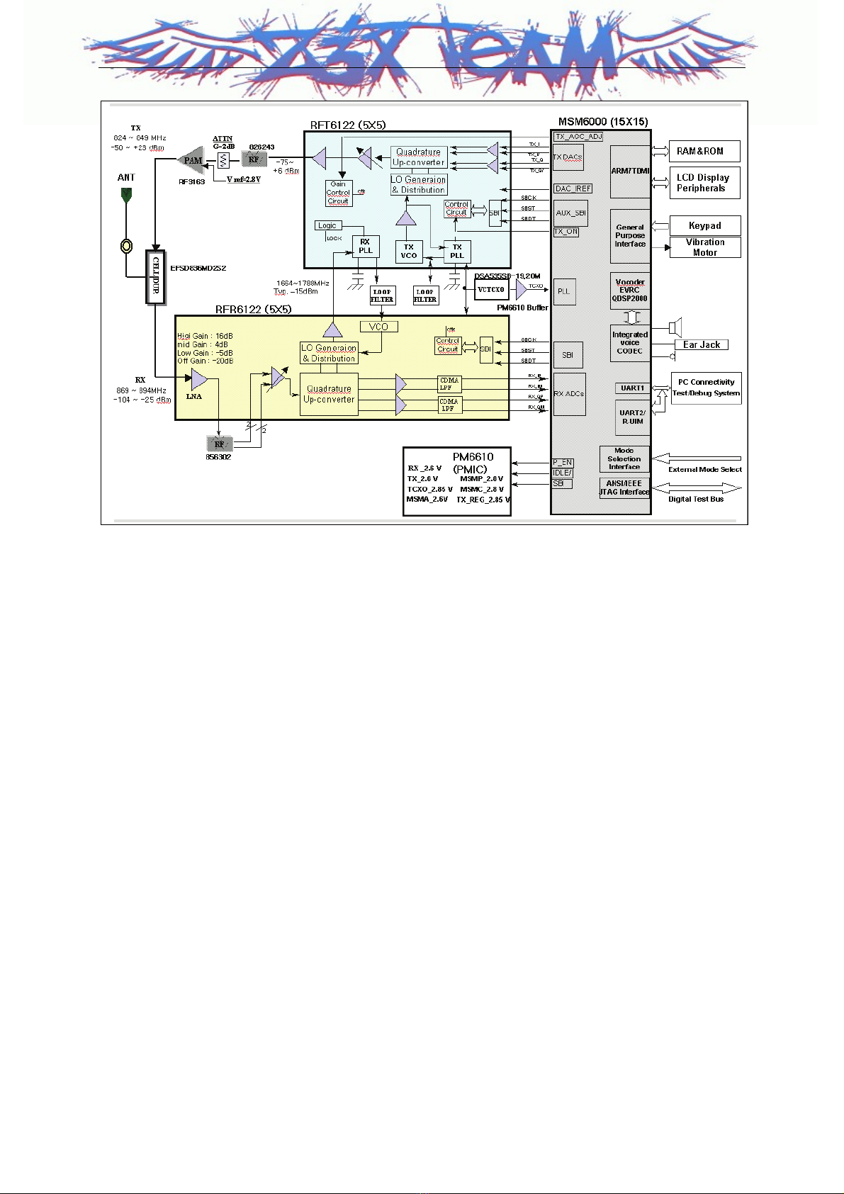
2.3.2 MSM Part
MSM6000 is the core element of a CDMA mobile station. Subsystems within the MSM6000 include a
CDMA processor, an EVRC(Enhanced Variable Rate Codec) vocoder, an ARM7TDMI
microprocessor ,and assorted peripheral interfaces that are used to support other functions.
MSM6000, when operated in the CDMA mode, utilizes CHIP×8 (9.8304MHz) as the reference clock
primarily for CDMA and vocoder processing.MSM6000 also uses TCXO/4 (4.92MHz).
The CPU controls total operations of the subscriber unit. Digital voice data, that have been inputted,
are encoded using the EVRC algorithm. Then, they are convolutionally encoded so that error
detection and correction are possible. Coded symbols are interleaved in order to avoid a burst error.
Each data channel is scrambled by the long code PN sequence of the user in order to ensure the
confidentiality of calls.
Moreover, binary quadrature codes are used based on Walsh functions in order to discern each
channel. Data created thus are 4-phase modulated by one pair of Pilot PN code and they are used to
create I and Q data.
When received, I and Q data are demodulated into symbols by the demodulator and then,
de-interleaved in reverse to the case of transmission. Then, the errors of data received from Viterbi
decoder are detected and corrected. They are voice decoded at the vocoder in order to output digital
voice data.
The MSM6000 also supports Enhanced Variable Rate Coder (EVRC) operation in addition to the
standard 8k.
2.3.2.1 Audio Processing Part
MIC signals are inputted into the audio codec, and amplified with programmable gain, and converted
into digital signals(PCM). Then, they are inputted into MSM6000.
In addition, digital audio signals(PCM) outputted from MSM6000 are converted into analog signals
after going through the audio codec. These signals are amplified with programmable gain on codec’s
internal AMP and external Audio AMP and then transferred to the ear piece. The signals is generated
in MSM6000 using SW MIDI.
2.3.3 Memory Part
The memory part consists of a 32Mbits Flash Memory and a 16Mbits SRAM. In the Flash Memory,
there are programs used for the operation of a mobile station. The programs can be changed through
down loading after the assembling of mobile stations. The Flash memory is also emulated as an
EEPROM to store ESN(Electronic Serial Number), Calibration Data, etc. On the SRAM, data
generated during the operation of a mobile station are stored temporarily.
7
Z3X-BOX.COM

LG-MC2670
2.3.4 Power Supply Part
Turn ON
When the battery voltage (4.2V ~ 3.3V) is fed and the PWR key of keypad is pressed, PMIC is
activated by the ON_SW signal, and then the control signal ON_SW_S/ signal is generated. And then,
the regurator 2.4V_MSMC & 2.8V_MSMP, 2.6V_MSMA, are operated.
Operating
During the phone is on operating state,
LDO(in PMIC) for MSM is always enable and gives the power MSM6000 and memory part
LDO(in PMIC) for +2.6V_TX part is enabled on IDLE/ state, and gives the power TX part devices.
LDO(in PMIC) for +2.6V_RX part is enabled on SLEEP/ state, and gives the power RX part devices.
Turn OFF
When the PWR key is pressed during a few seconds, PMIC is turned on by ON_SW and then, 'Low' is
outputted on ON_SW_S/. MSM6000 receives this signal and then, recognizes that the POWER key
has been pressed. During this time, MSM6000 outputs PS_HOLD as low and turn off all devices
[Figure 1-2] Block Diagram Of Power Management IC
2.3.5 Logic Part
The Logic part consists of internal CPU of MSM6000, PSEUDO RAM & FLASH MEMORY.
The MSM6000 receives TCXO/4 clock(19.20Mz) and CHIPX8 clock signals, and then controls the
phone during the CDMA and the FM mode. The major components are as follows:
8
Z3X-BOX.COM

LG-MC2670
CPU : ARM7TDMI microprocessor core
MEMORY : •FLASH Memory : 32M bits (K8D3216UTC-TI07)
•SRAM : 16M bits (K1S161611A-FI70)
CPU
ARM7TDMI 32-bit microprocessor is used and CPU controls all the circuitry. Some of the features of
the ARM microprocessor include a 3 stage pipelined RISC architecture, both 32-bit ARM and 16bit
THUMB instruction setsm, a 32-bit address bus, and a 32-bit internal data bus.
FLASH Memory
Flash Memory is used to store the program of the mobile station. Using the down-loading program,
the program can be changed even after the mobile station is fully assembled.
Pseudo RAM
SDRAM is used to store the internal flag information, call processing data, and timer data.
KEYPAD
For key recognition, key matrix is setup using KEY_SENSE0-4_N signals and GPIO32~36 of output
ports of MSM6000. Backlight circuitry are included in the keypad for easy operation in the dark.
LCD MODULE
LCD module contains a controller which will display the information onto the LCD by 8-bit data from
the MSM.
It has MONO full graphic 120(W) X 64(H) dots
9
Z3X-BOX.COM

LG-MC26 70
START
Rx TEST SETUP(HHP)
- Test Channel : 384
E5515C Setup
- CH : 384
- Sector Power : -30 dBm
Spectrum Analyzer Setting
Oscilloscope Setting
1. Check
PMIC Circuit
2. Check
VCTCXO Circuit
3. Check
Rx VCO
5. Check
Duplexer
Mobile SW
6. Check
Rx I/Q data
Re-download SW, CAL
2.1.1 When Rx Power isn’t enough
Checking Flow
Test Point
Figure 2.1.1
2.1 Rx Part Trouble
1
2
3
4
5
PMIC Part
VCTCXO
RFR6000
Duplexer
4. Check
Control Signal
CHAPTER 2. Trouble Shooting
10
Z3X-BOX.COM

LG-MC26 70
2.1.3 Checking VCTCXO Circuit
Circuit Diagram
Test Point Checking Flow
Check X100 Pin 3
◆Refer to Graph 4-1(a)
Check X100 Pin 4
◆ Refer to Graph 4-1(b)
19.2MHz OK?
+2.85V_TCXO OK?
No
Yes VCTCXO Circuit is Ok
See next Page to check
Rx VCO
Check Q701
No
Yes Changing X100
X100. 3X100. 4
Figure 2.1.3
Waveform
Graph 2.1.1(a) Graph 2.1.1(b)
U400. 32
12
Z3X-BOX.COM

LG-MC26 70
2.1.4 Checking Rx VCO Signal
Test Point
Checking Flow
Check U106 Pin 18
Check if there is
Any Major Difference
◆Refer to Graph 4-2
Check U106 Pin 16
Check if the voltage is
around 1.5V
UHF_LO OK?
CP_RX OK?
No
Yes
Yes
No
Rx VCO is Ok
See next Page
to check Control Signal
Check U105
Figure 2.1.4
Rx TEST SETUP(HHP)
- Test Channel : 384(DCN)
Spectrum Analyzer Setting
Oscilloscope Setting
U106.18 (UHF_LO_OUT)
U106.16 (CP_RX)
Replace U106
13
Z3X-BOX.COM

LG-MC26 70
2.1.5 Checking Control Signal
Test Point
Checking Flow
Waveform
U106. 3 (SBDT)U106. 4 (SBCK)
U106. 5 (SBST)
Check Pin 3, 4, 5
◆Refer to Graph 4-3(a,b)
Check SBDT, SBCK SBST
Check if there is
Any Major Difference
◆ Refer to Graph 4-3(a,b)
Level is High?
Similar?
Yes
No
Yes
No
Download the SW
Download the SW
Control Signal is Ok
See next Page to check
Duplexer
Figure 4-5
SBDT
SBCK SBCK
SBST
Graph 2.1.3(a) Graph 2.1.3(b)
15
Z3X-BOX.COM

LG-MC26 70
Checking Flow
Detected Signal?
No
Changing U100
Yes
Rx TEST SETUP(HHP)
- Test Channel : 384(DCN)
E5515C Setup
- CH : 384(DCN)
- Sector Power : -30 dBm
Spectrum Analyzer Setting
Oscilloscope Setting
Detected Signal?
Detected Signal?
DCN Duplexer is Ok
See next Page to check
Rx I/Q data Signal
Check C101
Changing DP101
Check U100 Pin 1
Check if there is
Any Major Difference
◆ Refer to Graph 4-4(a)
Check DP101 Pin 8
Check if there is
Any Major Difference
◆ Refer to Graph 4-4(b)
Check DP101 Pin 5
Check if there is
Any Major Difference
◆ Refer to Graph 4-4(c)
Yes
No
Yes
No
Waveform
U100 Pin 1
Graph 2.1.4(a)
17
Z3X-BOX.COM
Table of contents
Other LG Telephone manuals