LIST
OF
ILLUSTRATIONS
FIGURE
PAGE
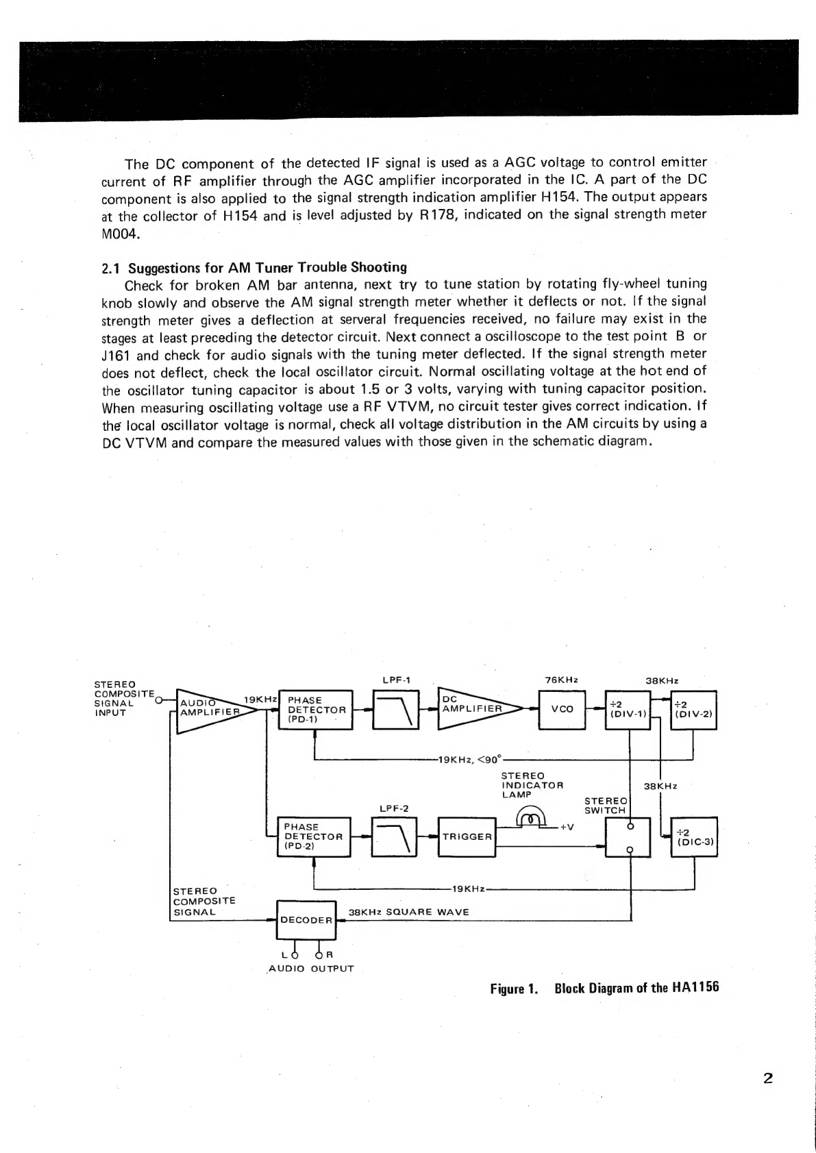
1.
Block
Diagram
of
the
HA1156
-+
+++
-
cece cece
eee
cece
eee
eee
t
teen
enn
ees
2
2.
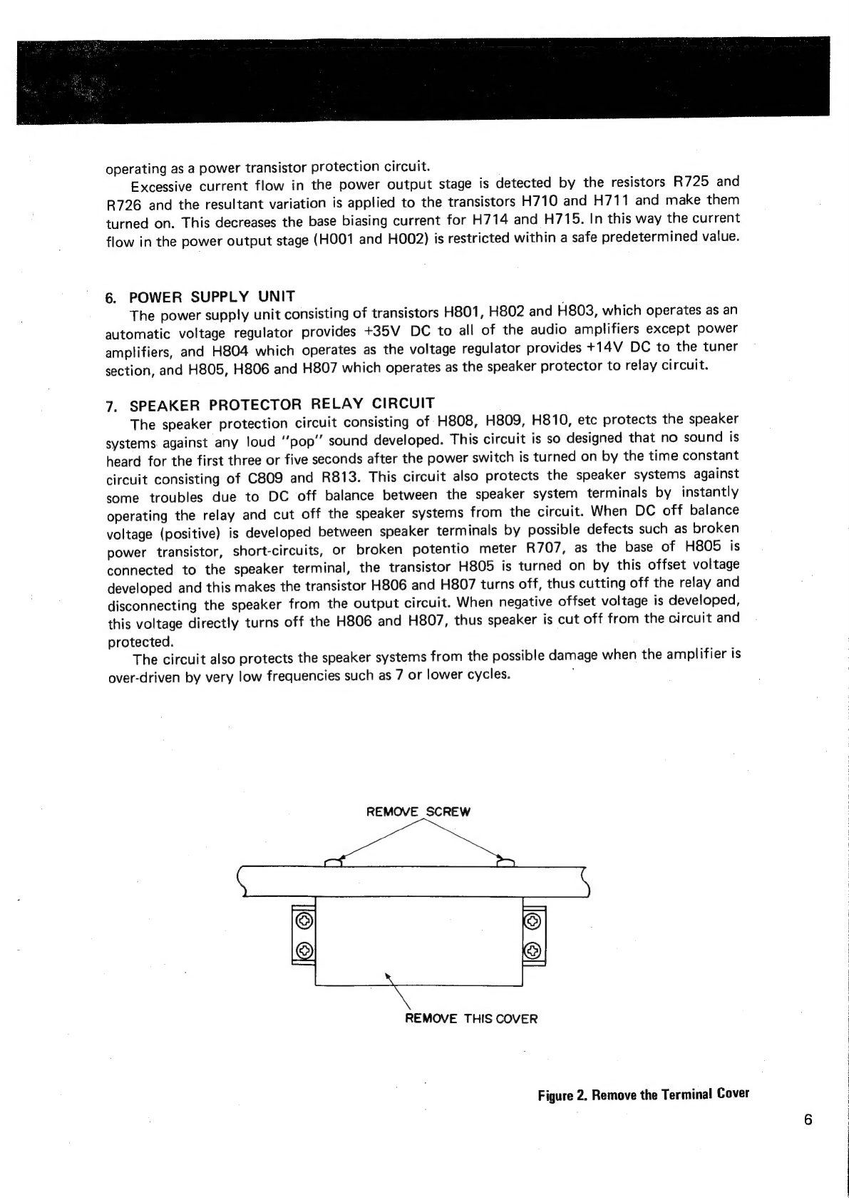
Remove
the
Terminal
Cover
---
+:
este
eect
tect
teen
eee
e
teen
e
ra
nnene
nes
6
3.
Dial
Stringing
«<-+
++
eect
teeta
eae
ee
ee
ree
ere
ae
11
4.
Front
Panel
Adjustment
and
Component
Locations
«++
-+++++ttrrrrtttr
ttre
tees
12
5.
Main
Chassis
Component
Locations
(Top
View)
«--+
str
trt
cst
s
ttt
tsetse
12
6.
Rear
Panel
Adjustment
and
Component
Locations
«+++
:ssstst
srt
rst
te
eres
13
7.
Main
Chassis
Component
Locations
(Bottom
View)
-c+ctttt
ttt
ttrtttrrtttees
13
8.
FM
Front
End
Assembly
P100
Component
Locations
«+++
++++ssttr
rrr
testes
14
9.
AM
Tuner
Unit
Assembly
P150
Component
Locations
<«-+:--:+++sessteet
tere
ees
14
10.
FMIF
Amplifier
Assembly
P200
Component
Locations
-+-+-+-++trttrrttttt
tees
15
11.
MPX
Stereo
Decoding
Amplifier
Assembly
P300
Components
Locations
-«+:+++e++e:
15
12.
Phono
Amplifier
Assembly
P400
Component
Locations
-++++++seeee
terre
eee
eens
16
13.
Power
Amplifier
Assembly
P700
Component
Locations
............0cece
eee
e
cues
16
14.
Power
Supply
Assembly
P800
Component
Locations
...........0cceceeeeeeeuees
17
15.
Dolby
Level
Assembly
PCO1
Component
Locations
..........0ecceceeeeeeueees
17
16.
Dial
Lamp
Assembly
PZ01
Component
Locations
..........-.eeeeeeeeeeeeeeees
18
17.
Functions
Lamp
Assembly
PYO1
Component
Locations
...........0.0ee
erences
18
18.
Pre-Tone
Amplifier
Assembly
PEO1
Component
Locations
.............0e00ee
eee
18
19.
High
and
Low
Filter
and
Muting
Switch
Unit
Assembly
PHO1
Component
Locations...
19
20.
Monitor
Dolby
Assembly
PTO1
Component
Locations
..........
0. ec
eee
eee
eee
19
21.
ANT.
Muting
Assembly
PUO1
Component
Locations
..............22200eeeeeeee
20
22.
Exploded
Mechanical
Diagram...
ee
eee
ee
eee
ete
t
teeter
neee
22
23.
Schematic
Diagram
++
+++
+s
eee
eee
eee
tte
een
ene
cence
ee ee
eens
24
24,
Rear
Panel
Adjustments
and
Component
Locations
for
European
Model
....
a
eieaindaa
te
39
25.
Main
Chassis
Component
Locations
(Bottom
View)
for
European
Model............
39
26:
‘Voltage
Conversion
Chart®
4c
fc
sixes
ceed
eta
ses
busted
ba
ed
eee
Vea
eee
es
40
27.
Schematic
Diagram
for
European
Model
........--
+.
eee
eee
eee
e
eee
enes
aa
latecoune
42