sees
eserneets
TABLE
OF
CONTENTS
SECTION
PAGE
VEACFOGUCTIONN
oe
ieibececcdieesseerientscesciecavceasasscttecdeusctsdacdadcaccceticacsesatecdtvancdescscbencsevdndaacnocounassescaeacde
1
Service
Notes
--s--ceseececccncccucccccseccccssccecccessceenetensseeceaentecesseesccesenesesnenaceseerennee
neue
eunseescenesesennes
1
PAM
Tuner
—
coccoccvarccccencccccccccnnsanssanssscancnsuccesesenecepecerersunrersaescsceusesesessene
neces
ses
nanenncuessenranncese
neg
1
PIV
Tinh
ectdestisesecccaiteanscatecds
cucecsee
ecoadeasuceiteusceuscecscedsconscusctcstocacsecsscueecestsedsaddsccevaeesideceecse
2
Phono
and
Tone
Amplifiers
a
Wie
u
Waveho
vnhek
Gite
be
sedis
vis
veueu
Fs
URUHN
donee
Da
NNN
ErOEs
cone
Rie
bayes
Resets
Ncdeweseieancass
5
Power
Amplifier
---+:---+--+sssssreseseneescensnarescennansnensceessansesenscsucensenessesasseceuesnsseusenecantoneasseesenses
5
Power
Protection
Circuit
—
<sressecescceceneceensccecnnensnenececensarensssenscunsnenansncussaucsananereseseaueaaucuseasaes
6
Speaker
Protector
Relay
Circuit
----+ssssesssessesseesesesscnssesseseeesstenenasenssssssnseusesenuensanesaeenegs
6
Suggestions
for
Troubleshooting
the
Power
Amplifier
—-------secsssseseseeeeceenseneresenenaesenserersens
6
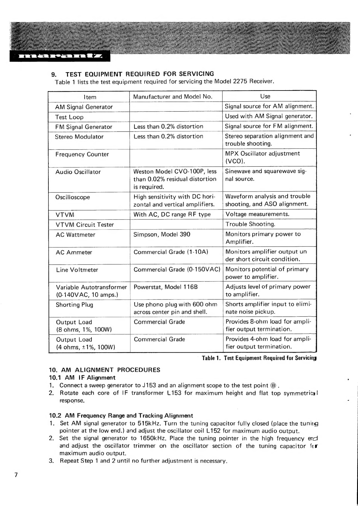
Test
Equipment
Required
FOr
SErViCiAG
---re-reecee
seven
enceenstecteceeetseeeneeeeseneneesenceenssnnconcneenseneane
7
AM
Alignment
Procedures
«:+:ssesesseessecsseecenteesnensncnercenenrensnscnenenennseecacecaeauanen
seusneeauaneguecenneges
7
FM
Alignment
Procedures
—
-+:-:+++++sssceeceeeeneesenscceeessrasenesnecceecansscerneeneeseensecaeenssenseeseagecssensrents
8
Stereo
Separation
Alignment
--+++--sscecceerseceeteeeceeeenennenensenceneneneeeensennasssecsecencaneneeneeeaeeaoannenens
8
Muting
Circuit
Alignment
—-ss::cscssssccscseecseseeneesnsnreeeseenerecanseesenaneeaeancensassnectenseacsonenansgenereeeas
8
FM
Dolby
Level
Adjustment
----scccssssseccsccsseerecensssnceeenseeceeenenseanseenanascenaansnsenaneeeaaeaseseone
nets
9
AUCIO
ACJUSTMENTS
—-vserereececeeceeerecansenentaencnenstecaseeatetensneceuaccustenseusasensceececaseustenaasensersranssees
9
Parts
List:
©
<isdvseiccececceccen
cies
dens
sonst
cee
cnc
ccecn
sped
sad
sedacvenccqccseneseceeceatescstac
etccetasniceostecueeswcasteesses
20~32
Technical
Specifications
.---+-s.secseccccsseecrenereesessesnssssnessnensnecensnnenerensasenntanencaneasensaccenenoaenenees
33~34
Servicing
Informations
for
European
Model
—
----ssssesscectesesseesseeseeesenssneseeeeeeennstaanenees
35~37,39
LIST
OF
ILLUSTRATIONS
FIGURE
PAGE
1.
Block
Diagram
OF
the:
HA1156
. ©
-wcisseveccs
dice
eeseeate
caress
dccsecelavedesssovedennsandievasaseveaveadeuess
4
2.
Dial
Stringing
--scrccceesscccceenccccceesnseeecnensanuecnececcueeescuanecesarasuceuecaseeseeeenensnteesssesnssenenapeeteneaes
10
3.
Front
Panel
Adjustments
and
Component
LOCATIONS:
Seseewssse
cs
ches
ccscenelecvecetaiic
cocdeceactscasede
11
4.
Main
Chassis
Component
Locations
(Top
VICW)
-onsecsenceseenccsecceccnerenseentcnseeeeseucnscesenrenneras
11
5.
Rear
Panel
Jacks
and
Component
LOCATIONS:
ssesetecide
secs
desaccscecsaacessws
dcctenducevcccvecaneaensesenes
12
6.
Main
Chassis
Component
Locations
(BOttOM
View)
—
-sscccccsersscnsercersnsecesecesensucesonseeseeeeoar
12
7.
FM
Front
End
Assembly
P100
Component
POCATIONS:
©
cieesesdsccesesces
cecccscdteesi
cies
egacvesseess
13
8.
AM
Tuner
Assembly
P150
Component
LOCATIONS
sseseesisees
dens
ccceecdvccsccnavecvecadetsevaasireeane
13
9.
FM
IF
Amplifier
Assembly
P200
Component
Locations
—
--+::::sseseeserseeteensserererenenensanees
13
10.
MPX
Stereo
Decoding
Amplifier
Assembly
P300
Component
Locations
—-+--+++-+seseeseeees
14
11.
Dolby
FM
Level
Amplifier
Assembly
PCO1
Component
Locations
—-ssreeceeesesseeserstsensees
14
12.
Phono
Amplifier
Assembly
P400
Component
Locations
—
«.+++.::ssseeeeseestsesrenssrnsenenannennees
14
13.
Power
Amplifier
Assembly
P700
Component
Locations
—
----+sssseseeesssceeeseeeceeseneeneneneeenes
15
14.
Power
Supply
and
Protection
Relay
Circuit
Assembly
P800
Component
Locations
15
15,
Pre
and
Tone
Amplifier
Assembly
PEO1
Component
Locations
«--++-++ssessseesssenseneeeterenees
16
16.
Dolby
FM,
Mono
L,
R,
Multipath
and
Tape
Monitor
Switches
Assembly
PSO1
Component
Locations
—.......ccccecceesssconseeceeneceeeseeensseseceseecnensseesoacaaccecsssseeeeeassesessaees
16
17.
Muting,
Speaker,
Loudness,
Power,
Hi
and
Low
Filter
Switches
PT0O1
Component
Locations
—
...ccccceececessseceereeeceseseseseessauenececaueenseseseeeaentecseeseeasesseescusngesseseesees
16
18.
Function
Lamps
Assembly
PY01
Component
Locations
—........cecscccessesecscseceeseeseesesssnacs
17
19.
Muting
Level
and
Antenna
Attenuator
Assembly
PUO1
Component
LOCATIONS”
_-eessevebek.
cctsteeese
elie
laste
ated
adaciidecc
onda
cde
edad
veclaas
vwedaswardecdeuabieesidvaaibovaenedacesesndens
17
20
_
Dial
Scale
Illuminator
Assembly
PZ01
Component
Locations
—.........scssssessesceeeeeeseseneeee
17
21.
Exploded
Mechanical
Diagram
—
...........cecssesesessescncnsnescceecceseceeaasaaessssssessessrsasessuesseses
18~19