TABLE
OF
CONTENTS
~
Section
.
7
Page
Wo
PAN
BOARDS:
6.
oe
mei
baa
Sey
Bing
cea
atv
uf
diab
dnie
Gaines
vait
ash
ogked
aiareetthee
Be
1
2.
TEST
EQUIPMENT
REQUIRED
FOR
SERVICING
..............
0.
cc
cece
cee
ee
cee
eauce
1
3.
FREQUENCY
SYNTHESIZER
RADIO
TUNING
SYSTEM
..........
0200-00
eeu
eeeueee
2
4;
ALIGNMENT
PROCEDURES
©.
a...
ye.ctiraowaiis
sis
eg
Was
oes
ek
angie
a
gti@e
Bw
aa
aa
aele
_
11
5.
VOLTAGE
CONVERSION
.......
0...
0...
0.
cece
ce
ee
cee
ee
eee
eee
F
ateiecey
Aces
Meta
esw
8
14
Gi.
“BLOCK.
DIAGRADMD
sicicsico
seats
awe
ie
Be
dates
eee
eet
dca
Stennett
do
anat's
fe
anand
eb
Sv
ages
Seadene
a
avetedecbkcs
15
7.
DIAGRAM
AND
COMPONENT
LOCATIONS...
.uiescgaa
wei
hoodie
ob
eed
ob
eee
16
7.4
Tuner/Phono
Amp.
{P100)
Schematic
Diagram
and
Component
Locations
............000eceaeue
16
7.2
Filter/Loudness
(PSQ0}
Schematic
Diagram
and
Component
Locations
...........00-0+eccueues
16
73
Head
Phone
{PWO1)
Schematic
Diagram
and
Component
Locations
.....
eee
iyein
isda
a
acan
eae
ete
ne
Biacieteee
18
7.4
Timer
Switch
(PS56)
Schematic
Diagram
and
Component
Locations
....
.
fp
evel
iel
ale
finite
OL.
0
UE)
Arata
rete
8
75
Tape
Monitor
Switch
(PJO0}
Schematic
Diagram
and
Component
Locations
........
0.0.06
.0eee
ee
18
7.6
Controller
(P500}
Schematic
Diagram
and
Component
Locations
........,.2.000ceceeceuccnaue
19
V7
PLL/L.P.F.
(P501)
Schematic
Diagram
and
Component
Locations
....-....-5
0.000
ce
eae
cuucece
19
7.8
VEFL/Signal
LED
{P502}
Schematic
Diagram
and
Component
Locations.
.........0.2.
0000
ce
eceue
19
7.9
EQ
Out
{PK00}
Schematic
Diagram
and
Component
Locations
..........00
0. cc
eeu
ecu
weevace
21
7.10
C/F
Display
(PU50)
Schematic
Diagram
and
Component
Locations.
............000ee00
05
eaters
21
7.11
Vol/Valance
(PGO0O}
Schematic
Diagram
and
Component
Locations
..........00.
00
cece
ac
cuaue
21
7.12
Function
Switch
(PU00}
Schematic
Diagram
and
Component
Locations
........0.2
0
ccc
ee ee
sees
21
7.13
Main
Amp.
{P701)
Schematic
Diagram
and
Component
Locations
........0.00
000
eee
ee
eaees
22
7.14
Main
Amp,
(P700)
Schematic
Diagram
and
Component
Locations.
...........
00000
cecedecaeee
22
7.15
Key
Board
Switch
(PTO00)
Schematic
Diagram
and
Component
Locations....:.........000.
ere
22
7.16
Power
Off
Switch
(PT50)
Schematic
Diagram
and
Component
Locations
.............000050-
nae
23
7.17
Scan
Step
Switch
(PC50)
Schematic
Diagram
and
Component
Locations
............000ceeeceas
23
7.18
Speaker
Protector
(PLOG)
Schematic
Diagram
and
Component
Locations
............-
cece
eceeue
23
7.19
Tone
Amp.
(PE00)
Schematic
Diagram
and
Component
Locations
..........-.00
cue
eueeeucune
24
7.20
Speaker
Switch
(PSO1t}
Schematic
Diagram
and
Component
Locations.............0ceeseeeeaae
24
7.21
Connection
(PEO1)
Schematic
Diagram
and
Component
Locations
...........0.0
ccc
cee
ee
avece
24
7.22
Tone
Amp.
(PEO2}
Schematic
Diagram
and
Component
Locations
............-..000cees
Batis
24
7.23
AC
Power
Relay
(PQ00)
Schematic
Diagram
and
Component
Locations............
taslal
a,
Bea
een
ane
i
25
7.24
Power
Supply
{P800)
Schematic
Diagram
and
Component
Locations.........-0...0
ce eee
eee
ace
25
7.25
Tone
Volume
(PEO3)
Schematic
Diagram
and
Component
Locations.
..........0.-.
cece
eeeeeae
26
7.26
Controller/Fip
(P503)
Schematic
Diagram
and
Component
Locations
............2-00cceeeueae
26
7.27
-
Controller/PLL
(P504)
Schematic
Diagram
and
Component,
LOGAtIONS
os
ie
ek
886
e
i068
ow
ete
ees
26
8.
EXPLODED
VIEW
AND
PARTS
LIST...
ce
ce
cc
ee
ee
teen
en
ues
27
9.
TECHNICAL
SPECIFICATIONS
.....
cc
ce
eee
eee
i
3
Pisa
ooay
env
acate
45
10./
SCHEMATIC:
DIAGRAM,
©
aici
4
oie
sciaien
we
ae
ORE
Ae
ase
ea
ee
ee
ET
AR
obG
o
owow
res
46
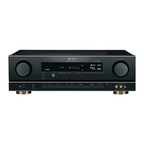
MODEL
SR8100DC
STEREOPHONIC
RECEIVER
Basa"


