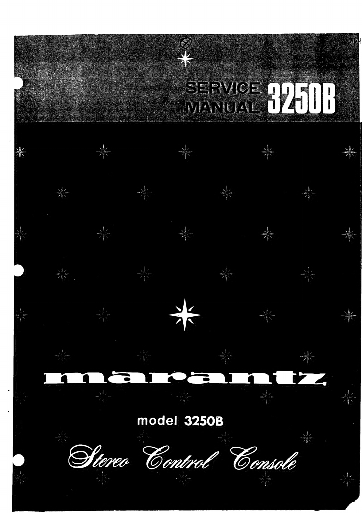
Marantz 3250B User manual
Other Marantz Recording Equipment manuals

Marantz
Marantz DR110 User manual

Marantz
Marantz Model 7 User manual

Marantz
Marantz PMD222 User manual

Marantz
Marantz CDR310 User manual

Marantz
Marantz PMD560 User manual

Marantz
Marantz PMD660 User manual

Marantz
Marantz PMD670 User manual

Marantz
Marantz PMD-602A User manual

Marantz
Marantz CDR420 User manual

Marantz
Marantz CDR310 User manual

Marantz
Marantz CDR310 User manual

Marantz
Marantz PMD570 User manual

Marantz
Marantz DR4160/F1N User manual

Marantz
Marantz Professional PMD661 User manual

Marantz
Marantz SX-72 User manual

Marantz
Marantz CDR620 User manual

Marantz
Marantz CDR631 User manual

Marantz
Marantz PMD570 User manual

Marantz
Marantz 4D Audio Dub Stations User manual

Marantz
Marantz DR6000 User manual