Maxim Integrated
│
2
www.maximintegrated.com
Evaluates: MAX17572 in 3.3V
Output-Voltage Application
MAX17572 3.3V Output
Evaluation Kit
Detailed Description of Hardware
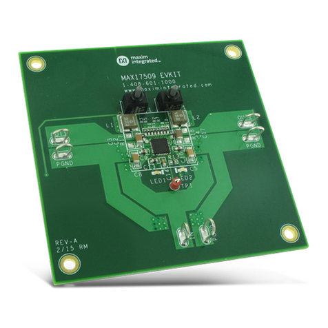
The MAX17572 3.3V output EV kit provides a proven
design to evaluate the MAX17572 high-voltage, high
efciency, synchronous step-down DC-DC converter. The
EV kit is preset for 3.3V output from 4.5V to 60V input at
load currents up to 1A and features a 500kHz switching
frequency for optimum efciency and component size.
The EV kit includes an EN/UVLO PCB pad and jumper
JU1 to enable the output at a desired input voltage. An
additional RESET PCB pad is available for monitoring
whether the converter output is in regulation.
Soft-Start capacitor selection
The device implements adjustable soft-start operation to
reduce inrush current. A capacitor connected from the SS
pin to GND programs the soft-start time. The selected
output capacitance (CSEL) and the output voltage (VOUT)
determine the minimum required soft-start capacitor
as follows:
6
SS SEL OUT
C 56 10 C V
−
≥× × ×
The soft-start time (tSS) is related to the capacitor con-
nected at SS (CSS) by the following equation:
SS
SS 6
C
t5.55 10−
=
×
For example, to program a 2ms soft-start time, a 12nF
capacitor should be connected from the SS pin to GND.
Setting the Undervoltage-Lockout Level
The device offers an adjustable input undervoltage-lockout
level. Set the voltage at which the device turns on with
a resistive voltage-divider connected from VIN to SGND
(see Figure 1). Connect the center node of the divider to
EN/UVLO. Choose R1 to be 3.3MΩ and then calculate
R2 as follows:
INU
1.215 R1
R2 (V 1.215)
×
=
−
where VINU is the voltage at which the device is required
to turn on. Ensure that VINU is higher than 0.8 x VOUT.
If the EN/UVLO pin is driven from an external signal source,
a series resistance of minimum 1kΩ is recommended to
be placed between the signal source output and the EN/
UVLO pin, to reduce voltage ringing on the line.
Adjusting Output Voltage
Set the output voltage with a resistive voltage-divider
connected from the positive terminal of the output capacitor
(VOUT) to SGND (see Figure 2). Connect the center node
of the divider to the FB pin. Use the following procedure to
choose the resistive voltage-divider values:
Calculate resistor R3 from the output to the FB pin as
follows:
OUT_SEL
1850
R3 C
=
Where COUT_SEL (in µF) is the actual derated value of
the output capacitance used and R3 is in kΩ. The minimum
allowable value of R3 is (5.6 x VOUT), where R3 is in kΩ.
If the value of R3 calculated using the above equation.
is less than (5.6 x VOUT), increase the value of R3 to at
least (5.6 x VOUT).
OUT
R3 0.9
R4 (V 0.9)
×
=
−
R4 is in kΩ.
Table 1. Regulator Enable (EN/UVLO) Description (JU1)
SHUNT POSITION EN/UVLO PIN MAX17572_ OUTPUT
1-2* Connected to VIN Enabled
Not installed Connected to the center node of resistor-divider
R1 and R2
Enabled, UVLO level set through the
R1 and R2 resistors
2-3 Connected to SGND Disabled
