MPS EVBL2166-D-00A User manual
EVBL2166-D-00A
6V, Dual 2A/2A or 3A/1A,
Low Quiescent Current,
Synchronous Buck with PG and SS
Evaluation Board
EVBL2166-D-00A Rev. 1.1 www.MonolithicPower.com 1
9/21/2020 MPS Proprietary Information. Patent Protected. Unauthorized Photocopy and Duplication Prohibited.
© 2020 MPS. All Rights Reserved.
DESCRIPTION
The EVBL2166-D-00A is an evaluation board
for the MP/MPQ2166 with MPS power inductor
stuffed.
MP/MPQ2166 is an internally compensated,
dual, PWM, synchronous, step-down regulator,
which operates from a 2.7V to 6V input and
generates an output voltage as low as 0.6V. It
can be configured as a 2A/2A or 3A/1A output
current regulator and is ideal for powering
portable equipment that runs on a single-cell
lithium-ion (Li+) battery due to a low 60µA
quiescent current.
The MP2166/MPQ2166 integrates dual, 55m,
high-side switches and 20msynchronous
rectifiers for high efficiency without an external
Schottky diode. The MP2166/MPQ2166 has
peak-current-mode control and internal
compensation and is capable of low dropout
configurations. Both channels can operate at
100% duty cycle.
Full protection features include cycle-by-cycle
current limit and thermal shutdown.
The EVBL2166-D-00A is assembled and tested
with QFN-18 (2mmX3mm) package.
ELECTRICAL SPECIFICATIONS
Parameter Symbol Value Units
Input Voltage VIN 2.7-6 V
Output Voltage VOUT1/ VOUT2 1.8/1.2 V
Output Current IOUT1/ IOUT2 2/2 A
3/1
FEATURES
2.7V to 6V Operating Input Range
2A/2A or 3A/1A Continuous Current
55m/20mRDS(ON)
Programmed Frequency up to 3MHz
External Sync Clock Up to 3MHz
180oPhase Shifted Operation
PG Indicators
External SS and Track
Adjustable Advanced Asynchronous Mode
(AAM) or Forced Continuous Conduction
Mode (CCM)
Output Adjustable from 0.6V to VIN
100% Duty Cycle Operation
Cycle-by-Cycle Over-Current Protection
(OCP)
Short-Circuit Protection (SCP) with Hiccup
Mode and Valley Current Detection
Thermal Shutdown
Fully Assembled and Tested
MPS Power Inductor Stuffed
APPLICATIONS
Small/Handled Devices
DVD Drivers
Smartphones and Feature Phones
Battery-Powered Devices
Portable Instruments
A
ll MPS parts are lead-free, halogen-free, and adhere to the RoHS directive.
For MPS green status, please visit the MPS website under Quality
A
ssurance. “MPS”, the MPS logo, and “Simple, Easy Solutions” are
trademarks of Monolithic Power Systems, Inc. or its subsidiaries.

EVBL2166-D-00A – 6V, DUAL 2A/2A OR 3A/1A, SYNCHRONOUS BUCK EV BOARD
EVBL2166-D-00A Rev. 1.1 www.MonolithicPower.com 2
9/21/2020 MPS Proprietary Information. Patent Protected. Unauthorized Photocopy and Duplication Prohibited.
© 2020 MPS. All Rights Reserved.
EVBL2166-D-00A EVALUATION BOARD
(L x W x H) 2.5” x 2.5” x 0.2”
(6.35cm x 6.35cm x0.5cm)
Board Number MPS IC Number
EVBL2166-D-00A MP/MPQ2166GD

EVBL2166-D-00A – 6V, DUAL 2A/2A OR 3A/1A, SYNCHRONOUS BUCK EV BOARD
EVBL2166-D-00A Rev. 1.1 www.MonolithicPower.com 3
9/21/2020 MPS Proprietary Information. Patent Protected. Unauthorized Photocopy and Duplication Prohibited.
© 2020 MPS. All Rights Reserved.
EVALUATION BOARD SCHEMETIC
1
2
3
4
13
12
11
10
5
6
PGND1
SW1
VIN1
FB1
FB2
VIN2
SW2
PGND2
7
8
9
18
17
16
15
14
SS1
PG1
FREQ
PG2
SS2
EN2
CCM
AGND
EN1
VCC
MPQ2166
22uF
C1A
16V
22uF
16V
2.7V-6V
EN2
0.1uF
C1B
16V
EN1
100k
R10 100k
R9
75k
R11
C4
50V
C3
JP1
VCC
AGND
CCMAAM
10
R7
100k
R8
C1C C1D
22uF
C2C
22uF
C2D
Vout2 1.5uH
L2
10
R5
100k
R6
22uF
C2A
Vout1
1.5uH
L1
22uF
C2B
VCC
0805 0805 0805 0805
0603 0603
0603
0603
0603
0603
0603
16V 16V
0805 0805
16V 16V
0805 0805
1.5nF
0603
50V
1.5nF
0603
1.2V/2A 1.8V/2A
100k
R3
0603 100K
R1
0603
NS
R4
0603
NS
R2
0603
0.1uF
16V
VIN
VEMI
GND
NS
CIN4
NS
FB1
47uF
CIN5
NS
L3
NS
CIN3
NS
CIN1
NS
CIN2
0603
0.1uF
C5
CHB CHA
NC
R13
NC
C9
NC
R14
NC
C10
100k
R12
0603
49.9k
R18
0603
NC
C6 C7
NC
NC
C11
R17
NC
C8
R19
R16
100k
NC
R15
100k
NC
PG2 PG1
Soft-Start:
1.5nF ->0.28ms
4.7nF->0.88ms
10nF -> 1.88ms
Tss= Css[nF]*Vref(0.6V)/ Iss(3.2uA)ms
Input EMC Filter
High if Vout
within +/-10%
R11 Fsw
665k350kHz
200k1MHz
75k2.25MHz
51k3MHz
Vout (V) R6/R8 (k) R18/R12 (k)
3.3 100 (1%) 22.1 (1%)
1.8 100 (1%) 49.9 (1%)
1.2 100 (1%) 100 (1%)
PGND1
SW1
VIN1
FB1
FB2
VIN2
SW2
PGND2
SS1
PG1
FREQ
PG2
SS2
EN2
CCMAGND
EN1
VCC
17
18
16
15
14
6
5
7
8
9
3
4
2
11
10
13
12
1
Package Reference
0.6V
0.6V
2.25MHz
EN high: 1.6V
EN low: 0.4V
CIN5 is for damping
input C and L
EVBL2166-D-00A BILL OF MATERIALS
Qty Ref Value Description Package Manufacturer Manufactuer_P/N
4 CIN1,CIN2,
CIN3,CIN4 NS
1 FB1 NS
1 L3 NS
1 CIN5 47F Electrolytic
Capacitor; 16V SMD Jianghai VZ1-16V47
6
C1A, C1D,
C2A, C2B,
C2C, C2D
22F Ceramic
Capacitor;16V;X5R 0805 muRata GRM21BR61C226ME44L
2 C1B, C1C 0.1FCeramic
Capacitor;16V;X7R 0805 muRata GRM219R71C104KA01D
2 C3, C4 1.5nF Ceramic
Capacitor;50V;X7R 0603 muRata GRM188R71H153KA01D
EVBL2166-D-00A – 6V, DUAL 2A/2A OR 3A/1A, SYNCHRONOUS BUCK EV BOARD
EVBL2166-D-00A Rev. 1.1 www.MonolithicPower.com 4
9/21/2020 MPS Proprietary Information. Patent Protected. Unauthorized Photocopy and Duplication Prohibited.
© 2020 MPS. All Rights Reserved.
EVBL2166-D-00A BILL OF MATERIALS (continued)
Qty Ref Value Description Package Manufacturer Manufactuer_P/N
1 C5 0.1F Ceramic
Capacitor;16V;X5R 0603 muRata GRM188R61C104KA01D
6 C6, C7, C8,
C9, C10, C11 NS
2 L1, L2 1.5H Inductor; 14.5m;
6.4A SMD MPS MPL-AL4020-1R5
9
R1, R3, R6,
R8, R9, R10,
R12,
R17,R19
100k Film Resistor;1%; 0603 Yageo RC0603FR-07100KL
2 R5,R7 10 Film Resistor;1%; 0603 Yageo RC0603FR-0710RL
1 R18 49.9k Film Resistor;1%; 0603 Yageo RC0603FR-07105KL
6
R2, R4, R13,
R14,
R15,R16
NS
1 R11 75k Film Resistor;1%; 0603 Yageo RC0603FR-0775KL
1 U1
Step-Down
Converter QFN-18 MPS MP2166GD
7
VIN, VEMI,
GND,
VOUT1,
GND,
VOUT2, GND
Test
Point 2.0 Golden Pin HZ
9
PG2, GND,
EN2, EN1,
GND, PG1,
JP1
2.54mm Test Pin any

EVBL2166-D-00A – 6V, DUAL 2A/2A OR 3A/1A, SYNCHRONOUS BUCK EV BOARD
EVBL2166-D-00A Rev. 1.1 www.MonolithicPower.com 5
9/21/2020 MPS Proprietary Information. Patent Protected. Unauthorized Photocopy and Duplication Prohibited.
© 2020 MPS. All Rights Reserved.
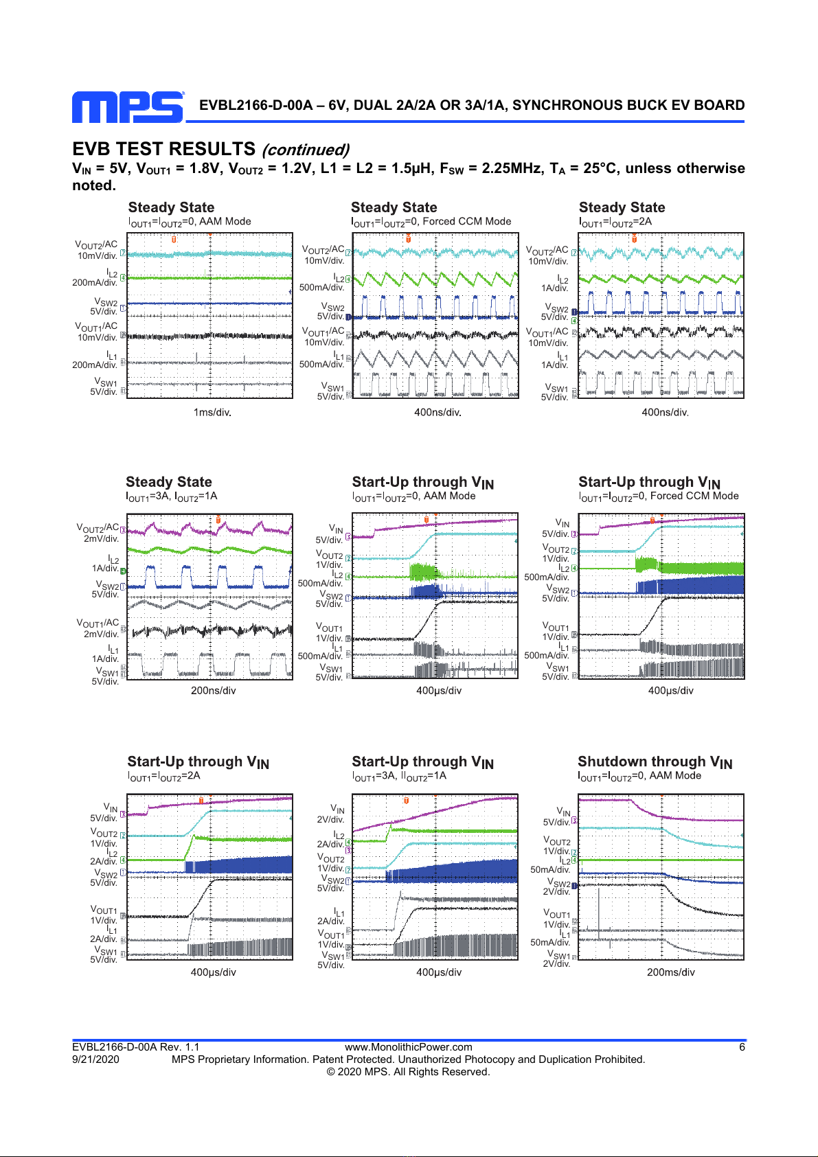
EVB TEST RESULTS
VIN = 5V, VOUT1 = 1.8V, VOUT2 = 1.2V, L1 = L2 = 1.5µH, FSW = 2.25MHz, TA= 25°C, unless otherwise
noted.
EVBL2166-D-00A – 6V, DUAL 2A/2A OR 3A/1A, SYNCHRONOUS BUCK EV BOARD
EVBL2166-D-00A Rev. 1.1 www.MonolithicPower.com 6
9/21/2020 MPS Proprietary Information. Patent Protected. Unauthorized Photocopy and Duplication Prohibited.
© 2020 MPS. All Rights Reserved.
EVB TEST RESULTS
(continued)
VIN = 5V, VOUT1 = 1.8V, VOUT2 = 1.2V, L1 = L2 = 1.5µH, FSW = 2.25MHz, TA= 25°C, unless otherwise
noted.
V
OUT2
/AC
10mV/div.
V
OUT1
/AC
10mV/div.
V
SW1
5V/div.
V
SW2
5V/div.
I
L1
200mA/div.
I
L2
200mA/div.
V
OUT2
/AC
10mV/div.
V
OUT1
/AC
10mV/div.
V
SW1
5V/div.
V
SW2
5V/div.
I
L1
500mA/div.
I
L2
500mA/div.
V
OUT2
/AC
2mV/div.
V
OUT2
1V/div.
V
IN
5V/div.
V
OUT1
/AC
2mV/div.
V
SW1
5V/div.
V
SW2
5V/div. V
SW2
5V/div.
I
L1
1A/div.
I
L2
1A/div. I
L2
500mA/div.
V
OUT1
1V/div.
V
SW1
5V/div.
I
L1
500mA/div.
V
OUT2
1V/div.
V
IN
5V/div.
V
SW2
5V/div.
I
L2
2A/div.
V
OUT1
1V/div.
V
SW1
5V/div.
I
L1
2A/div.
V
OUT2
1V/div.
V
IN
2V/div.
V
SW2
5V/div.
I
L2
2A/div.
V
OUT1
1V/div.
V
SW1
5V/div.
I
L1
2A/div.
V
OUT2
1V/div.
V
IN
5V/div.
V
SW2
5V/div.
I
L2
500mA/div.
V
OUT1
1V/div.
V
SW1
5V/div.
I
L1
500mA/div.
V
OUT2
/AC
10mV/div.
V
OUT1
/AC
10mV/div.
V
SW1
5V/div.
V
SW2
5V/div.
I
L1
1A/div.
I
L2
1A/div.
V
OUT2
1V/div.
V
IN
5V/div.
V
SW2
2V/div.
I
L2
50mA/div.
V
OUT1
1V/div.
V
SW1
2V/div.
I
L1
50mA/div.

EVBL2166-D-00A – 6V, DUAL 2A/2A OR 3A/1A, SYNCHRONOUS BUCK EV BOARD
EVBL2166-D-00A Rev. 1.1 www.MonolithicPower.com 7
9/21/2020 MPS Proprietary Information. Patent Protected. Unauthorized Photocopy and Duplication Prohibited.
© 2020 MPS. All Rights Reserved.
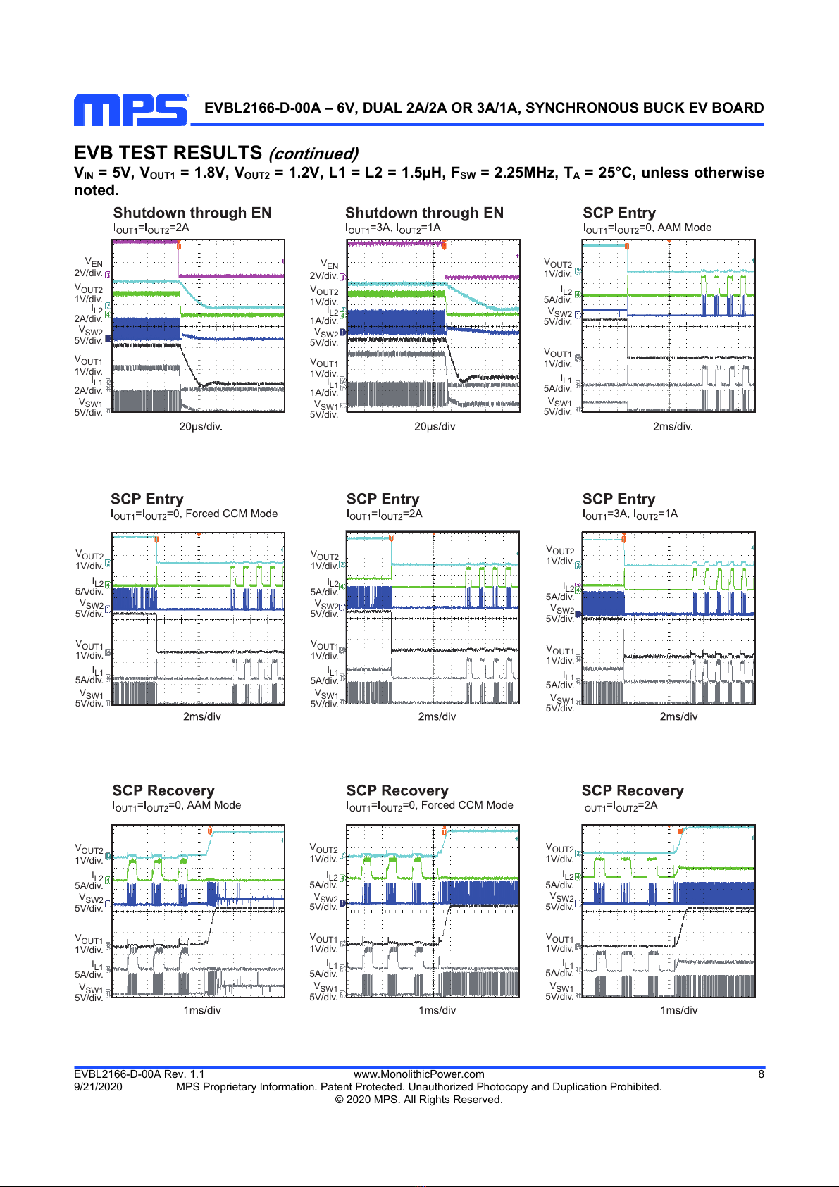
EVB TEST RESULTS
(continued)
VIN = 5V, VOUT1 = 1.8V, VOUT2 = 1.2V, L1 = L2 = 1.5µH, FSW = 2.25MHz, TA= 25°C, unless otherwise
noted.
VOUT2
1V/div.
VEN
2V/div.
VSW2
5V/div.
IL2
500mA/div.
VOUT1
1V/div.
VSW1
5V/div.
IL1
500mA/div.
VOUT2
1V/div.
VEN
2V/div.
VSW2
5V/div.
IL2
500mA/div.
VOUT1
1V/div.
VSW1
5V/div.
IL1
500mA/div.
VOUT2
1V/div.
VEN
2V/div.
VSW2
5V/div.
IL2
1A/div.
VOUT1
1V/div.
VSW1
5V/div.
IL1
1A/div.
VOUT2
1V/div.
VEN
2V/div.
VSW2
2V/div.
IL2
50mA/div.
VOUT1
1V/div.
VSW1
2V/div.
IL1
50mA/div.
VOUT2
1V/div.
VEN
2V/div.
VSW2
5V/div.
IL2
500mA/div.
VOUT1
1V/div.
VSW1
5V/div.
IL1
500mA/div.
VOUT2
1V/div.
VEN
2V/div.
VSW2
5V/div.
IL2
2A/div.
VOUT1
1V/div.
VSW1
5V/div.
IL1
2A/div.
VOUT2
1V/div.
VIN
5V/div.
VSW2
5V/div.
IL2
500mA/div.
VOUT1
1V/div.
VSW1
5V/div.
IL1
500mA/div.
VOUT2
1V/div.
VIN
5V/div.
VSW2
5V/div.
IL2
2A/div.
VOUT1
1V/div.
VSW1
5V/div.
IL1
2A/div.
VOUT2
1V/div.
VIN
2V/div.
VSW2
5V/div.
IL2
1A/div.
VOUT1
1V/div.
IL1
1A/div.
EVBL2166-D-00A – 6V, DUAL 2A/2A OR 3A/1A, SYNCHRONOUS BUCK EV BOARD
EVBL2166-D-00A Rev. 1.1 www.MonolithicPower.com 8
9/21/2020 MPS Proprietary Information. Patent Protected. Unauthorized Photocopy and Duplication Prohibited.
© 2020 MPS. All Rights Reserved.
EVB TEST RESULTS
(continued)
VIN = 5V, VOUT1 = 1.8V, VOUT2 = 1.2V, L1 = L2 = 1.5µH, FSW = 2.25MHz, TA= 25°C, unless otherwise
noted.
V
OUT2
1V/div.
V
SW2
5V/div.
I
L2
5A/div.
V
OUT1
1V/div.
V
SW1
5V/div.
I
L1
5A/div.
V
OUT2
1V/div.
V
SW2
5V/div.
I
L2
5A/div.
V
OUT1
1V/div.
V
SW1
5V/div.
I
L1
5A/div.
V
OUT2
1V/div.
V
SW2
5V/div.
I
L2
5A/div.
V
OUT1
1V/div.
V
SW1
5V/div.
I
L1
5A/div.
V
OUT2
1V/div.
V
SW2
5V/div.
I
L2
5A/div.
V
OUT1
1V/div.
V
SW1
5V/div.
I
L1
5A/div.
V
OUT2
1V/div.
V
SW2
5V/div.
I
L2
5A/div.
V
OUT1
1V/div.
V
SW1
5V/div.
I
L1
5A/div.
V
OUT2
1V/div.
V
SW2
5V/div.
I
L2
5A/div.
V
OUT1
1V/div.
V
SW1
5V/div.
I
L1
5A/div.
V
OUT2
1V/div.
V
SW2
5V/div.
I
L2
5A/div.
V
OUT1
1V/div.
V
SW1
5V/div.
I
L1
5A/div.
V
OUT2
1V/div.
V
EN
2V/div.
V
SW2
5V/div.
I
L2
2A/div.
V
OUT1
1V/div.
V
SW1
5V/div.
I
L1
2A/div.
V
OUT2
1V/div.
V
EN
2V/div.
V
SW2
5V/div.
I
L2
1A/div.
V
OUT1
1V/div.
V
SW1
5V/div.
I
L1
1A/div.

EVBL2166-D-00A – 6V, DUAL 2A/2A OR 3A/1A, SYNCHRONOUS BUCK EV BOARD
EVBL2166-D-00A Rev. 1.1 www.MonolithicPower.com 9
9/21/2020 MPS Proprietary Information. Patent Protected. Unauthorized Photocopy and Duplication Prohibited.
© 2020 MPS. All Rights Reserved.
EVB TEST RESULTS
(continued)
VIN = 5V, VOUT1 = 1.8V, VOUT2 = 1.2V, L1 = L2 = 1.5µH, FSW = 2.25MHz, TA= 25°C, unless otherwise
noted.
V
OUT1
/AC
200mV/div.
V
SW1
5V/div.
I
L1
2A/div.
V
OUT2
/AC
100mV/div.
V
SW2
5V/div.
I
L2
2A/div.
V
OUT2
1V/div.
V
SW2
5V/div.
I
L2
5A/div.
V
OUT1
1V/div.
V
SW1
5V/div.
I
L1
5A/div.
V
SW1
5V/div.
I
L1
2A/div.
V
SW2
5V/div.
I
L2
2A/div.
V
OUT1
/AC
100mV/div.
V
SW1
5V/div.
I
L1
1A/div.
V
OUT2
/AC
100mV/div.
V
SW2
5V/div.
I
L2
1A/div.
V
OUT1
/AC
200mV/div.
V
SW1
5V/div.
I
L1
2A/div.
V
OUT2
/AC
200mV/div.
V
SW2
5V/div.
I
L2
2A/div.
V
OUT1
/AC
100mV/div.
V
SW1
5V/div.
I
L1
1A/div.
V
OUT2
/AC
100mV/div.
I
L2
1A/div.

EVBL2166-D-00A – 6V, DUAL 2A/2A OR 3A/1A, SYNCHRONOUS BUCK EV BOARD
EVBL2166-D-00A Rev. 1.1 www.MonolithicPower.com 10
9/21/2020 MPS Proprietary Information. Patent Protected. Unauthorized Photocopy and Duplication Prohibited.
© 2020 MPS. All Rights Reserved.
PRINTED CIRCUIT LAYOUT
Figure 1: Top & TOP Silk Layer Figure 2: Inner1 Layer
Figure 3: Inner2 Layer Figure 4: Bottom & Bottom Silk Layer

EVBL2166-D-00A – 6V, DUAL 2A/2A OR 3A/1A, SYNCHRONOUS BUCK EV BOARD
NOTICE: The information in this document is subject to change without notice. Please contact MPS for current specifications.
Users should warrant and guarantee that third party Intellectual Property rights are not infringed upon when integrating MPS
products into any application. MPS will not assume any legal responsibility for any said applications.
EVBL2166-D-00A Rev.1.1 www.MonolithicPower.com 11
9/21/2020 MPS Proprietary Information. Patent Protected. Unauthorized Photocopy and Duplication Prohibited.
© 2020 MPS. All Rights Reserved.
QUICK START GUIDE
1. Connect the positive and negative terminals of the load to the VOUT and GND pins, respectively.
Be aware that electronic loads represent a negative impedance to the regulator and if set to a too
high current will trigger Hiccup mode.
2. Preset the power supply output to expected value (2.7V-6V), and then turn it off.
3. Connect the positive and negative terminals of the power supply output to the VIN and GND pins,
respectively.
4. Turn the power supply on (the MP/MPQ2166GD will automatically startup).
5. To get better EMI performance, add the EMI components at bottom layer of the board and connect
the input power supply between VEMI and GND.
6. To use the Enable function, apply a digital input to the EN pin. Drive EN higher than 1.6V to turn on
the regulator, drive EN less than 0.4V to turn it off. EN can also be connected to VIN directly if don’t
use the Enable function.
7. A resistor is connected between FREQ and GND to set up the internal oscillator frequency. FREQ
can also be used to synchronize the internal oscillator to an external clock. The rising edge of the
channel 1 clock is synchronized to the external clock rising edge, while the channel 2 clock remains
at 180°out-of-phase to channel 1. The recommended external SYNC frequency is in the range of
350kHz to 3MHz.
8. An AAM mode or forced CCM mode can be selected at JP1.
9. The soft-start time can also be programmed by an external capacitor connected to SS, shown in
Equation (1):
AI
VVnFC
mst
SS
RFFSS
SS
Where CSS is the external SS capacitor, VREF is the internal reference voltage (0.6V), and ISS is the 3.2µA
SS charge current. The soft-start time is about 0.5ms when SS pin is floating.
10. Use R6(R8) and R18(R12) to set the output voltage with VFB=0.6V. For R6(R8)=100k, R18(R12)
can be determined by:
OUT
R6(R8)
R18(R12)= V-1
0.6
Follow the Application Information section in the device datasheet to recalculate the compensation,
inductor and output capacitor values when output voltage is changed.
EVBL2166-D-00A – 6V, DUAL 2A/2A OR 3A/1A, SYNCHRONOUS BUCK EV BOARD
NOTICE: The information in this document is subject to change without notice. Please contact MPS for current specifications.
Users should warrant and guarantee that third party Intellectual Property rights are not infringed upon when integrating MPS
products into any application. MPS will not assume any legal responsibility for any said applications.
EVBL2166-D-00A Rev.1.1 www.MonolithicPower.com 12
9/21/2020 MPS Proprietary Information. Patent Protected. Unauthorized Photocopy and Duplication Prohibited.
© 2020 MPS. All Rights Reserved.
Revision History
Revision # Revision
Date Description Pages
Updated
1.0 10/17/2019 Initial Release -
1.1 9/21/2020
Correct the inductor part number from “MPL-AY4020-
1R5” to “MPL-AL4020-1R5” in the BOM. P4
Table of contents
Other MPS Motherboard manuals


MPS
MPS EV2605DQ-00B User manual

MPS
MPS EVHR2000-S-00A User manual

MPS
MPS EVKT-MP8833 User manual

MPS
MPS EVKT-MP8860 User manual

MPS
MPS MagAlpha EVMA Q-00A Series Operating instructions

MPS
MPS EVKT-MACOM User manual

MPS
MPS MP2483 User manual

MPS
MPS EV2696A-Q-00B User manual

MPS
MPS EV6001DN-00D User manual

MPS
MPS EV0035 User manual


