IBM PPC750FX User manual

PPC750FX Evaluation Board
User’s Manual
SA14-2720-00
Preliminary
une 10, 2003
Title Page

®
© Copyright International Business Machines Corporation 2002, 2003
All Rights Reserved
Printed in the United States of America une 2003
The following are trademarks of International Business Machines Corporation in the United States, or other countries, or
both:
Other company, product, and service names may be trademarks or service marks of others.
The information contained in this document is subject to change or withdrawal at any time without notice and is
being provided on an "AS IS" basis without warranty or indemnity of any kind, whether e press or implied,
including without limitation, the implied warranties of non-infringement, merchantability, or fitness for a
particular purpose. Any products, services, or programs discussed in this document are sold or licensed under
IBM's standard terms and conditions, copies of which may be obtained from your local IBM representative.
Nothing in this document shall operate as an e press or implied license or indemnity under the intellectual
property rights of IBM or third parties.
Without limiting the generality of the foregoing, any performance data contained in this document was
determined in a specific or controlled environment and not submitted to any formal IBM test. Therefore, the
results obtained in other operating environments may vary significantly. Under no circumstances will IBM be
liable for any damages whatsoever arising out of or resulting from any use of the document or the information
contained herein.
IBM Microelectronics Division
1580 Route 52, Bldg. 504
Hopewell unction, NY 12533-6351
The IBM home page can be found at http://www.ibm.com
The IBM Microelectronics Division home page can be found at http://www.ibm.com/chips
750FXebm_title.fm
une 10, 2003
IBM PowerPC Architecture PPC750FX
IBM logo PowerPC Embedded Controllers RISCTrace
PowerPC PowerPC logo RISCWatch
Note: This document contains information on products in the sampling and/or initial production phases of
development. This information is subject to change without notice. Verify with your IBM field applications
engineer that you have the latest version of this document before finalizing a design.
While the information contained herein is believed to be accurate, such information is preliminary, and should not be
relied upon for accuracy or completeness, and no representations or warranties of accuracy or completeness are made.

Evaluation Board Manual
Preliminary PPC750FX Evaluation Board
750FXebmTOC.fm
une 10, 2003
Contents
Page 3 of 115
Contents
Tables . . . . . . . . . . . . . . . . . . . . . . . . . . . . . . . . . . . . . . . . . . . . . . . . . . . . . . . . . . . . . . . 7
Figures . . . . . . . . . . . . . . . . . . . . . . . . . . . . . . . . . . . . . . . . . . . . . . . . . . . . . . . . . . . . . . 9
About This Book . . . . . . . . . . . . . . . . . . . . . . . . . . . . . . . . . . . . . . . . . . . . . . . . . . . . . 11
1. Overview . . . . . . . . . . . . . . . . . . . . . . . . . . . . . . . . . . . . . . . . . . . . . . . . . . . . . . . . . . 13
1.1 PowerPC 750FX RISC Microprocessor Features . . . . . . . . . . . . . . . . . . . . . . . . . . . . . . . . . . . 13
1.2 Board Features . . . . . . . . . . . . . . . . . . . . . . . . . . . . . . . . . . . . . . . . . . . . . . . . . . . . . . . . . . . . . 17
2. Board Design . . . . . . . . . . . . . . . . . . . . . . . . . . . . . . . . . . . . . . . . . . . . . . . . . . . . . . 19
2.1 Processor . . . . . . . . . . . . . . . . . . . . . . . . . . . . . . . . . . . . . . . . . . . . . . . . . . . . . . . . . . . . . . . . . . 19
2.2 Board Clocking . . . . . . . . . . . . . . . . . . . . . . . . . . . . . . . . . . . . . . . . . . . . . . . . . . . . . . . . . . . . . 20
2.3 Internal Processor Clocking . . . . . . . . . . . . . . . . . . . . . . . . . . . . . . . . . . . . . . . . . . . . . . . . . . . . 21
2.4 System Controller . . . . . . . . . . . . . . . . . . . . . . . . . . . . . . . . . . . . . . . . . . . . . . . . . . . . . . . . . . . 21
2.5 SDRAM Interface . . . . . . . . . . . . . . . . . . . . . . . . . . . . . . . . . . . . . . . . . . . . . . . . . . . . . . . . . . . . 21
2.6 PCI Bus . . . . . . . . . . . . . . . . . . . . . . . . . . . . . . . . . . . . . . . . . . . . . . . . . . . . . . . . . . . . . . . . . . . 21
2.7 Ethernet . . . . . . . . . . . . . . . . . . . . . . . . . . . . . . . . . . . . . . . . . . . . . . . . . . . . . . . . . . . . . . . . . . . 21
2.8 Flash Memory . . . . . . . . . . . . . . . . . . . . . . . . . . . . . . . . . . . . . . . . . . . . . . . . . . . . . . . . . . . . . . 22
2.9 NVRAM . . . . . . . . . . . . . . . . . . . . . . . . . . . . . . . . . . . . . . . . . . . . . . . . . . . . . . . . . . . . . . . . . . . 24
2.10 SRAM . . . . . . . . . . . . . . . . . . . . . . . . . . . . . . . . . . . . . . . . . . . . . . . . . . . . . . . . . . . . . . . . . . . 24
2.11 Serial Ports . . . . . . . . . . . . . . . . . . . . . . . . . . . . . . . . . . . . . . . . . . . . . . . . . . . . . . . . . . . . . . . 24
2.12 Logic Analyzer Connections . . . . . . . . . . . . . . . . . . . . . . . . . . . . . . . . . . . . . . . . . . . . . . . . . . 25
2.13 Power Supply . . . . . . . . . . . . . . . . . . . . . . . . . . . . . . . . . . . . . . . . . . . . . . . . . . . . . . . . . . . . . . 25
2.13.1 PCI Voltages . . . . . . . . . . . . . . . . . . . . . . . . . . . . . . . . . . . . . . . . . . . . . . . . . . . . . . . . . . . 25
2.13.2 System Controller Voltages . . . . . . . . . . . . . . . . . . . . . . . . . . . . . . . . . . . . . . . . . . . . . . . 25
2.13.3 PPC750FX Voltages . . . . . . . . . . . . . . . . . . . . . . . . . . . . . . . . . . . . . . . . . . . . . . . . . . . . . 25
2.13.4 SDRAM Voltages . . . . . . . . . . . . . . . . . . . . . . . . . . . . . . . . . . . . . . . . . . . . . . . . . . . . . . . 26
2.14 Form Factor . . . . . . . . . . . . . . . . . . . . . . . . . . . . . . . . . . . . . . . . . . . . . . . . . . . . . . . . . . . . . . . 26
3. Memory Map . . . . . . . . . . . . . . . . . . . . . . . . . . . . . . . . . . . . . . . . . . . . . . . . . . . . . . . 27
3.1 CPLD Register Definitions . . . . . . . . . . . . . . . . . . . . . . . . . . . . . . . . . . . . . . . . . . . . . . . . . . . . 27
4. Programming the System Controller . . . . . . . . . . . . . . . . . . . . . . . . . . . . . . . . . . . 31
4.1 DDR SDRAM . . . . . . . . . . . . . . . . . . . . . . . . . . . . . . . . . . . . . . . . . . . . . . . . . . . . . . . . . . . . . . 31
4.1.1 SDRAM Controller Initialization . . . . . . . . . . . . . . . . . . . . . . . . . . . . . . . . . . . . . . . . . . . . . 31
4.2 Device Controller Bank Register Settings . . . . . . . . . . . . . . . . . . . . . . . . . . . . . . . . . . . . . . . . . 31
4.2.1 Device Bank 0 Parameters (32-bit Flash) . . . . . . . . . . . . . . . . . . . . . . . . . . . . . . . . . . . . . . 32
4.2.2 Device Bank 1 Parameters (CPLD registers) . . . . . . . . . . . . . . . . . . . . . . . . . . . . . . . . . . . 33

Evaluation Board Manual
PPC750FX Evaluation Board Preliminary
Contents
Page 4 of 115
750FXebmTOC.fm
une 10, 2003
4.2.3 Device Bank 2 Parameters (UARTs) . . . . . . . . . . . . . . . . . . . . . . . . . . . . . . . . . . . . . . . . . 34
4.2.4 Device Bank 3 Parameters (FRAM) . . . . . . . . . . . . . . . . . . . . . . . . . . . . . . . . . . . . . . . . . . 35
4.2.5 Boot Device Parameters (8 bit flash and SRAM) . . . . . . . . . . . . . . . . . . . . . . . . . . . . . . . . 36
5. Reset and Interrupts . . . . . . . . . . . . . . . . . . . . . . . . . . . . . . . . . . . . . . . . . . . . . . . . . 37
5.1 Resets . . . . . . . . . . . . . . . . . . . . . . . . . . . . . . . . . . . . . . . . . . . . . . . . . . . . . . . . . . . . . . . . . . . . 37
5.2 Interrupts . . . . . . . . . . . . . . . . . . . . . . . . . . . . . . . . . . . . . . . . . . . . . . . . . . . . . . . . . . . . . . . . . . 37
6. Switches . . . . . . . . . . . . . . . . . . . . . . . . . . . . . . . . . . . . . . . . . . . . . . . . . . . . . . . . . . 39
6.1 Reset Pushbutton . . . . . . . . . . . . . . . . . . . . . . . . . . . . . . . . . . . . . . . . . . . . . . . . . . . . . . . . . . . 39
6.2 ATX Power-on Pushbutton . . . . . . . . . . . . . . . . . . . . . . . . . . . . . . . . . . . . . . . . . . . . . . . . . . . . 40
6.3 CPU 0 PLL Configuration . . . . . . . . . . . . . . . . . . . . . . . . . . . . . . . . . . . . . . . . . . . . . . . . . . . . . 40
6.4 CPU 1 PLL Configuration . . . . . . . . . . . . . . . . . . . . . . . . . . . . . . . . . . . . . . . . . . . . . . . . . . . . . 41
6.5 System Controller Initialization . . . . . . . . . . . . . . . . . . . . . . . . . . . . . . . . . . . . . . . . . . . . . . . . . 42
7. Fuses, Batteries, Regulators, and Fans . . . . . . . . . . . . . . . . . . . . . . . . . . . . . . . . . 45
7.1 On-Board Current Monitoring and Variable Voltage Testing . . . . . . . . . . . . . . . . . . . . . . . . . . 45
7.1.1 1.45V Supplies . . . . . . . . . . . . . . . . . . . . . . . . . . . . . . . . . . . . . . . . . . . . . . . . . . . . . . . . . . 45
7.1.2 2.5V Supply . . . . . . . . . . . . . . . . . . . . . . . . . . . . . . . . . . . . . . . . . . . . . . . . . . . . . . . . . . . . 46
7.2 Fan . . . . . . . . . . . . . . . . . . . . . . . . . . . . . . . . . . . . . . . . . . . . . . . . . . . . . . . . . . . . . . . . . . . . . . . 46
8. Displays . . . . . . . . . . . . . . . . . . . . . . . . . . . . . . . . . . . . . . . . . . . . . . . . . . . . . . . . . . . 47
9. Jumpers . . . . . . . . . . . . . . . . . . . . . . . . . . . . . . . . . . . . . . . . . . . . . . . . . . . . . . . . . . . 49
9.1 Write-Protect 32-Bit Flash . . . . . . . . . . . . . . . . . . . . . . . . . . . . . . . . . . . . . . . . . . . . . . . . . . . . . 50
9.2 Ignore Fan . . . . . . . . . . . . . . . . . . . . . . . . . . . . . . . . . . . . . . . . . . . . . . . . . . . . . . . . . . . . . . . . . 50
9.3 PCI Interrupt Selection . . . . . . . . . . . . . . . . . . . . . . . . . . . . . . . . . . . . . . . . . . . . . . . . . . . . . . . . 51
10. Connectors . . . . . . . . . . . . . . . . . . . . . . . . . . . . . . . . . . . . . . . . . . . . . . . . . . . . . . . 53
10.1 Auxiliary Power . . . . . . . . . . . . . . . . . . . . . . . . . . . . . . . . . . . . . . . . . . . . . . . . . . . . . . . . . . . . 55
10.2 Ground . . . . . . . . . . . . . . . . . . . . . . . . . . . . . . . . . . . . . . . . . . . . . . . . . . . . . . . . . . . . . . . . . . . 56
10.3 Fan Power . . . . . . . . . . . . . . . . . . . . . . . . . . . . . . . . . . . . . . . . . . . . . . . . . . . . . . . . . . . . . . . . 56
10.4 RISCWatch TAG Debugger . . . . . . . . . . . . . . . . . . . . . . . . . . . . . . . . . . . . . . . . . . . . . . . . . . 57
10.5 Ethernet . . . . . . . . . . . . . . . . . . . . . . . . . . . . . . . . . . . . . . . . . . . . . . . . . . . . . . . . . . . . . . . . . 58
10.6 PCI Connector . . . . . . . . . . . . . . . . . . . . . . . . . . . . . . . . . . . . . . . . . . . . . . . . . . . . . . . . . . . . . 59
10.7 CPLD TAG Connector . . . . . . . . . . . . . . . . . . . . . . . . . . . . . . . . . . . . . . . . . . . . . . . . . . . . . . 62
10.8 Serial Ports . . . . . . . . . . . . . . . . . . . . . . . . . . . . . . . . . . . . . . . . . . . . . . . . . . . . . . . . . . . . . . . 63
10.9 System Controller Device Address Bus . . . . . . . . . . . . . . . . . . . . . . . . . . . . . . . . . . . . . . . . . . 64
10.10 Memory Control . . . . . . . . . . . . . . . . . . . . . . . . . . . . . . . . . . . . . . . . . . . . . . . . . . . . . . . . . . . 66
10.11 External Clock Input . . . . . . . . . . . . . . . . . . . . . . . . . . . . . . . . . . . . . . . . . . . . . . . . . . . . . . . . 68
10.12 Test Connections . . . . . . . . . . . . . . . . . . . . . . . . . . . . . . . . . . . . . . . . . . . . . . . . . . . . . . . . . . 69

Evaluation Board Manual
Preliminary PPC750FX Evaluation Board
750FXebmTOC.fm
une 10, 2003
Contents
Page 5 of 115
11. CPLD Programming . . . . . . . . . . . . . . . . . . . . . . . . . . . . . . . . . . . . . . . . . . . . . . . 73
11.1 Programming—Registers and Control Functions . . . . . . . . . . . . . . . . . . . . . . . . . . . . . . . . . . 73
11.1.1 I/O Pin List . . . . . . . . . . . . . . . . . . . . . . . . . . . . . . . . . . . . . . . . . . . . . . . . . . . . . . . . . . . . 73
11.1.2 CPLD Logic . . . . . . . . . . . . . . . . . . . . . . . . . . . . . . . . . . . . . . . . . . . . . . . . . . . . . . . . . . . 76
11.1.2.1 Top Level Block Diagram 1 . . . . . . . . . . . . . . . . . . . . . . . . . . . . . . . . . . . . . . . . . . . . 77
11.1.2.2 Top Level Block Diagram 2 . . . . . . . . . . . . . . . . . . . . . . . . . . . . . . . . . . . . . . . . . . . . 78
11.1.2.3 framcs Logic . . . . . . . . . . . . . . . . . . . . . . . . . . . . . . . . . . . . . . . . . . . . . . . . . . . . . . . 79
11.1.2.4 decode_block Program . . . . . . . . . . . . . . . . . . . . . . . . . . . . . . . . . . . . . . . . . . . . . . . 80
11.1.2.5 registers2 Program . . . . . . . . . . . . . . . . . . . . . . . . . . . . . . . . . . . . . . . . . . . . . . . . . . 84
11.1.2.6 reset_block Program . . . . . . . . . . . . . . . . . . . . . . . . . . . . . . . . . . . . . . . . . . . . . . . . . 89
11.1.2.7 misc Logic . . . . . . . . . . . . . . . . . . . . . . . . . . . . . . . . . . . . . . . . . . . . . . . . . . . . . . . . . 93
11.2 Timing—Registers and Control Functions . . . . . . . . . . . . . . . . . . . . . . . . . . . . . . . . . . . . . . . . 94
11.2.1 Maximum Clock Frequency . . . . . . . . . . . . . . . . . . . . . . . . . . . . . . . . . . . . . . . . . . . . . . . 94
11.2.2 Clock-to-Output Time . . . . . . . . . . . . . . . . . . . . . . . . . . . . . . . . . . . . . . . . . . . . . . . . . . . . 94
11.2.3 Pin-to-Pin Signal Delay . . . . . . . . . . . . . . . . . . . . . . . . . . . . . . . . . . . . . . . . . . . . . . . . . . . 96
11.2.4 Setup and Hold Time . . . . . . . . . . . . . . . . . . . . . . . . . . . . . . . . . . . . . . . . . . . . . . . . . . . 100
12. Bills of Materials . . . . . . . . . . . . . . . . . . . . . . . . . . . . . . . . . . . . . . . . . . . . . . . . . . 101
12.1 Component Location . . . . . . . . . . . . . . . . . . . . . . . . . . . . . . . . . . . . . . . . . . . . . . . . . . . . . . . 101
12.2 Debugging Tools . . . . . . . . . . . . . . . . . . . . . . . . . . . . . . . . . . . . . . . . . . . . . . . . . . . . . . . . . . 104
12.3 Auxiliary Materials . . . . . . . . . . . . . . . . . . . . . . . . . . . . . . . . . . . . . . . . . . . . . . . . . . . . . . . . . 104
12.4 Board Bill of Materials . . . . . . . . . . . . . . . . . . . . . . . . . . . . . . . . . . . . . . . . . . . . . . . . . . . . . . 105
Inde . . . . . . . . . . . . . . . . . . . . . . . . . . . . . . . . . . . . . . . . . . . . . . . . . . . . . . . . . . . . . . 113
Revision Log . . . . . . . . . . . . . . . . . . . . . . . . . . . . . . . . . . . . . . . . . . . . . . . . . . . . . . . 115


Evaluation Board Manual
Preliminary PPC750FX Evaluation Board
750FXebmLOT.fm
une 10, 2003
Tables
Page 7 of 115
Tables
Table 2-1. Ethernet Ports ........................................................................................................................ 21
Table 2-2. Switch Settings ....................................................................................................................... 23
Table 2-3. Flash Configurations .............................................................................................................. 23
Table 3-1. Board Address Space Usage ................................................................................................. 27
Table 3-2. Register0 ................................................................................................................................ 27
Table 3-3. Register1 ................................................................................................................................ 28
Table 3-4. Register2 ................................................................................................................................ 28
Table 3-5. Register3 ................................................................................................................................ 29
Table 3-6. Register4 ................................................................................................................................ 29
Table 4-1. DDR SDRAM Characteristics ................................................................................................. 31
Table 4-2. Device Bank 0 Parameters = 0x85A492BF ........................................................................... 32
Table 4-3. Device Bank 1 Parameters = 0x8004921A ............................................................................ 33
Table 4-4. Device Bank 2 Parameters = 0x8C002BD6 ........................................................................... 34
Table 4-5. Device Bank 3 Parameters = 0x8D891445 ............................................................................ 35
Table 4-6. Boot Device Bank Parameters = 0x8185D09E ...................................................................... 36
Table 5-1. External Interrupts .................................................................................................................. 38
Table 6-1. Switches ................................................................................................................................. 39
Table 6-2. Reset Pushbutton—U5 .......................................................................................................... 39
Table 6-3. Reset Pushbutton—U53 ........................................................................................................ 40
Table 6-4. CPU 0 PLL Configuration—U30 ............................................................................................. 40
Table 6-5. CPU 1 PLL Configuration Switches—U35 ............................................................................. 41
Table 6-6. System Controller Initilization—U17 ....................................................................................... 42
Table 6-7. System Controller Initilization—U24 ....................................................................................... 43
Table 7-1. Current Measurement of the1.4V Supplies ............................................................................ 45
Table 7-2. Current Measurement of the 2.5V Supply ............................................................................. 46
Table 8-1. Displays ................................................................................................................................. 47
Table 9-1. umpers ................................................................................................................................. 49
Table 9-2. Write-Protect 32-bit Flash Memory— 8 ................................................................................. 50
Table 9-3. Ignore Fans— 16 ................................................................................................................... 50
Table 9-4. PCI Interrupt Selection— 22 .................................................................................................. 51
Table 10-1. Connectors ............................................................................................................................. 53
Table 10-2. ATX Power Signals— 34 ....................................................................................................... 55
Table 10-3. Ground Connectors — 1, 2, 7, 9, 10, 12, 17, 18, 23, 24 ....................................... 56
Table 10-4. Fan Power Signals— 4, ......................................................................................................... 56
Table 10-5. RISCWatch Signals— 11 ...................................................................................................... 57
Table 10-6. Ethernet UTP Signals— 20, both sockets ............................................................................. 58

Evaluation Board Manual
PPC750FX Evaluation Board Preliminary
Tables
Page 8 of 115
750FXebmLOT.fm
une 10, 2003
Table 10-7. PCI Connector Signals— 25 ..................................................................................................59
Table 10-8. CPLD TAG Connector— 26 .................................................................................................62
Table 10-9. Serial Port Connector Signals— 13, both ports .....................................................................63
Table 10-10. System Controller Device Address Signals— 14 ...................................................................64
Table 10-11. Memory Control Signals— 15 ................................................................................................66
Table 10-12. External Clock Input Signal—U39 ..........................................................................................68
Table 10-13. Test Connections ....................................................................................................................69
Table 11-1. Section Contents ....................................................................................................................73
Table 11-2. CPLD I/O Pin List ...................................................................................................................73
Table 11-3. CPLD Logic Descriptions ........................................................................................................76
Table 11-4. Maximum Clock Frequency ....................................................................................................94
Table 11-5. Clock-to-Output Time .............................................................................................................94
Table 11-6. Pin-to-Pin Signal Delay ...........................................................................................................96
Table 11-7. Setup and Hold Time ............................................................................................................100
Table 12-1. Section Contents ..................................................................................................................101
Table 12-2. Component Placement Data Description .............................................................................102
Table 12-3. Debugging Tools ..................................................................................................................104
Table 12-4. Auxiliary Materials in Kit .......................................................................................................104
Table 12-5. Evaluation Board Bill of Materials .........................................................................................106

Evaluation Board Manual
Preliminary PPC750FX Evaluation Board
750FXebmLOF.fm
une 10, 2003
Figures
Page 9 of 115
Figures
Figure 1-1. PPC750FX Block Diagram ..................................................................................................... 14
Figure 2-1. PPC750FX Board Architecture .............................................................................................. 19
Figure 2-2. Clock Distribution on the PPC750FX Board ........................................................................... 20
Figure 2-3. Board Ethernet Architecture ................................................................................................... 22
Figure 2-4. Board Serial Port Architecture ................................................................................................ 24
Figure 5-1. Interrupt Architecture .............................................................................................................. 37
Figure 6-1. Switch Location Diagram ....................................................................................................... 39
Figure 7-1. Resistor Location Diagram ..................................................................................................... 45
Figure 7-2. Fan and Heatsink Location Diagram ...................................................................................... 46
Figure 8-1. Display Location Diagram ...................................................................................................... 47
Figure 9-1. umper Location Diagram ...................................................................................................... 49
Figure 9-2. Write-Protect 32-bit Flash Memory umper— 8 .................................................................... 50
Figure 9-3. Ignore Fan umper— 16 ....................................................................................................... 50
Figure 9-4. PCI Interrupt Selection umper— 22 ..................................................................................... 51
Figure 10-1. Connector Location Diagram, Top Side ................................................................................. 54
Figure 10-2. ATX Power Supply Connector— 34 ......................................................................................55
Figure 10-3. Ground Connectors— 1, 2, 7, 9, 10, 12, 17, 18, 23, 24 ........................................ 56
Figure 10-4. Fan Power Connector— 4 ..................................................................................................... 56
Figure 10-5. RISCWatch TAG Connector— 11 ....................................................................................... 57
Figure 10-6. Ethernet Connector—One of two R 45 Sockets in 20 ......................................................... 58
Figure 10-7. PCI Connector— 25 ............................................................................................................. 59
Figure 10-8. CPLD TAG Connector— 26 ................................................................................................ 62
Figure 10-9. Serial Port Connector— 13, one of two R 11/12 sockets ..................................................... 63
Figure 10-10. System Controller Device Address Connector— 14 ............................................................. 64
Figure 10-11. Memory Control Connector— 15 ........................................................................................... 66
Figure 10-12. External Clock Input Connector—U39 ................................................................................... 68
Figure 10-13. Test Connection Locations ..................................................................................................... 71
Figure 12-1. Example of a Component Placement List in the Schematics ............................................... 102
Figure 12-2. Board Location Grid—Top View ........................................................................................... 103
Figure 12-3. Board Location Grid—Bottom View .....................................................................................103


Evaluation Board Manual
Preliminary PPC750FX Evaluation Board
750FXebm_preface.fm
une 10, 2003
About This Book
Page 11 of 115
About This Book
This manual describes an evaluation platform for the PPC750FX chip.
Who Should Use This Book
This book is written to aid programmers and other technical personnel in the use of the PPC750FX
Evaluation Board. In order to use the board and this document, the reader shouldbe familiar with the
following:
• PowerPC Architecture™
• PCI bus
• Embedded microprocessor hardware
• IBM RISCWatch™ debugger
How to Use This Book
This book describes the features and interfaces of the IBM PPC750FX Evaluation Board. This book contains
the following sections:
•Overview provides a brief overview of the processor chip. Some chip aspects important to understanding
the board design are discussed in greater detail.
•Board Design describes the architecture of the evaluation board.
•Memory Map describes the address space usage of the board. Tables are provided which define the
access methods for all memory-mapped registers on the board.
•Programming the System Controller outlines the required programming to configure the MV64360
system controller for the board memory and peripherals.
•Reset and Interrupts lists the sources of resets and interrupts on the board, and provides information
required to program the PPC750FX amd MV64360 interrupt controllers.
•Switches locates and describes the function of all switches on the board, and indicates their default
settings.
•Fuses, Batteries, Regulators, and Fans locates and describes the function of fuses, batteries, and
voltage regulator adjustments on the board.
•Displays locates and describes all displays on the board.
•umpers locates and describes all jumpers on the board, and indicates their default settings.
•Connectors locates and describes all connectors on the board, and identifies the pin usage.
•CPLD Programming provides the source code and timing information for the CPLDs on the board.
•Bills of Materials provides lists of materials and parts that are assembled on the board, parts shipped with
the board but not assembled on the board, and other tools that are useful while using the board.

Evaluation Board Manual
PPC750FX Evaluation Board Preliminary
About This Book
Page 12 of 115
750FXebm_preface.fm
une 10, 2003
Related Publications
The following publications contain related information:
• PowerPC 750FX RISC Microprocessor Embedded Controller Data Sheet
• PowerPC 750FX RISC Microprocessor Embedded Controller Functional Specification
• PowerPC 750FX RISC Microprocessor Embedded Controller User’s Manual
• PowerPC 750FX RISC Microprocessor Evaluation Design Kit User’s Manual
• PowerPC 750FX RISC Microprocessor Evaluation Board Schematics
• PowerPC Architecture
•PowerPC Microprocessor Family: The Programming Environments, MPRPPCFPE-01
•PowerPC Embedded Processor Solutions, SC09-3032, a CDROM which includes the RISCWatch
Debugger User’s Guide
• PowerPC CoreConnect Bus (PLB) Specification
• PCI Local Bus Specification
•Marvell
MV64360/1/2 Data Sheet

Evaluation Board Manual
Preliminary PPC750FX Evaluation Board
750FXebm_ch1.fm
une 10, 2003
Overview
Page 13 of 115
1. Overview
The PowerPC 750FX Evaluation Board is an evaluation platform intended to support the needs of
prospective users of the IBM PowerPC 750FX processor. The form factor of the board is a full-length PCI
card. This board is suitable for software development, for benchmarking, and for detailed study of the
hardware. This board contains two PPC750FX processors. A memory control and PCI bridge function
provided on the board coordinates the operations of the two processors. The two processors may be used
together or independently under program control. Both processors share the available memory and the PCI
interface. The board can appear to the PCI interface as either a 64-bit adapter or a 64-bit host.
Please be aware that the circuitry on this board is sometimes more complex than would be required for a
board design limited to a particular application. A customer who is developing his own design using this board
design as a guide should simplify the design wherever his application allows.
Warning: IBM is not responsible for use of the circuit designs on this board or use of the design of the
board itself in any other applications. Any functional, reliability, or safety issues resulting from the use of
any part of this board design, including copying the board, are the responsibility of the user.
The following sections will highlight the PPC750FX processor, and will then briefly discuss the features
available on the board.
1.1 PowerPC 750FX RISC Microprocessor Features
The IBM PowerPC 750FX RISC Microprocessor is a 32-bit implementation of the IBM PowerPC family of
reduced instruction set computer (RISC) microprocessors. The PPC750FX is targeted for high performance,
low power systems using a 60x bus. The 750FX also includes an internal 512KB L2 cache with on-board
Error Correction Circuitry (ECC). A block diagram of the processor chip is provided in Figure 1-1.
Evaluation Board Manual
PPC750FX Evaluation Board Preliminary
Overview
Page 14 of 115
750FXebm_ch1.fm
une 10, 2003
The PPC750FX processor has the following features:
• Branch processing unit
- Four instructions fetched per clock.
- One branch processed per cycle (plus resolving two speculations).
- Up to one speculative stream in execution, one additional speculative stream in fetch.
- 512-entry branch history table (BHT) for dynamic prediction.
- 64-entry, 4-way set associative branch target instruction cache (BTIC) for eliminating branch delay
slots.
• Dispatch unit
- Full hardware detection of dependencies (resolved in the execution units).
- Dispatch two instructions to six independent units (system, branch, load/store, fixed-point unit 1
(FXU1), fixed-point unit 2 (FXU2), or floating-point).
- Four-stage pipeline: fetch, dispatch, execute, and complete.
- Serialization control (predispatch, postdispatch, execution, serialization).
Figure 1-1. PPC750FX Block Diagram
FXU2 GPRs LSU FPU
Instruction Fetch
System
Completion
Rename
Buffers
Unit
32KB I-Cache
32KB D-Cache
BHT/BTIC
BIU
Enhanced
512KB
FXU1
L2 Tags
Dispatch
Branch Unit
Control Unit
FPRs
Rename
Buffers
with ECC
60X
with parity
with parity
L2 Cache

Evaluation Board Manual
Preliminary PPC750FX Evaluation Board
750FXebm_ch1.fm
une 10, 2003
Overview
Page 15 of 115
• Decode
- Register file access.
- Forwarding control.
- Partial instruction decode.
• Load/Store unit
- One cycle load or store cache access (byte, half word, word, double word).
- Effective address generation.
- Hits under misses (one outstanding miss).
- Single-cycle misaligned access within double word boundary.
- Alignment, zero padding, sign extend for integer register file.
- Floating-point internal format conversion (alignment, normalization).
- Sequencing for load/store multiples and string operations.
- Store gathering.
- Cache and translation look-aside buffer (TLB) instructions.
- Big and little-endian byte addressing supported.
- Misaligned little-endian support in hardware.
• Fixed-point units
- FXU1: multiply, divide, shift, rotate, arithmetic, logical.
- FXU2: shift, rotate, arithmetic, logical.
- Single-cycle arithmetic, shift, rotate, logical.
- Multiply and divide support (multi-cycle).
- Early out multiply.
- Thirty-two, 32-bit general purpose registers.
• Floating-point unit
- Support for IEEE-754 standard single- and double-precision floating-point arithmetic.
- Optimized for single-precision multiply/add.
- Thirty-two, 64-bit floating point registers.
- Enhanced reciprocal estimates.
- Three-cycle latency, one-cycle throughput, single-precision multiply-add.
- Three-cycle latency, one-cycle throughput, double-precision add.
- Four-cycle latency, two-cycle throughput, double-precision multiply-add.
- Hardware support for divide.
- Hardware support for denormalized numbers.
- Time deterministic non-IEEE mode.
• System unit
- Executes CR logical instructions and miscellaneous system instructions.
- Special register transfer instructions.
• Level 1 (L1) Cache structure
- 32KB, 32-byte line, 8-way set associative instruction cache.
- 32KB, 32-byte line, 8-way set associative data cache.
- Single-cycle cache access.

Evaluation Board Manual
PPC750FX Evaluation Board Preliminary
Overview
Page 16 of 115
750FXebm_ch1.fm
une 10, 2003
- Pseudo-LRU replacement.
- Copy-back or write-through data cache (on a page per page basis).
- Parity on L1 tags and arrays.
- Three-state (MEI) memory coherency.
- Hardware support for data coherency.
- Non-blocking instruction cache (one outstanding miss).
- Non-blocking data cache (two outstanding misses).
- No snooping of instruction cache.
• Memory management unit
- 64-entry, 2-way set associative instruction TLB (total 128).
- 64-entry, 2-way set associative data TLB (total 128).
- Hardware reload for TLB's.
- Eight instruction BAT's and eight data BATs.
- Virtual memory support for up to 4PB (252) virtual memory.
- Real memory support for up to 4GB (232) of physical memory.
- Support for big/little-endian addressing.
• Dual PLLs
- Allows seamless frequency switching.
• Level 2 (L2) cache
- Internal L2 cache controller and 4K-entry tags; 512KB data SRAMs.
- Two-way set associative, supports locking by way.
- Copy-back or write-through data cache on a page basis, or for all L2.
- 64-byte sectored line size.
- L2 frequency at core speed.
- ECC protection on SRAM array.
- Parity on L2 tags.
- Supports up to 2 outstanding misses (1 data and 1 instruction or 2 data).
• Bus interface
- 32-bit address bus.
- 64-bit data bus (can be operated in 32-bit mode).
- Core-to-bus frequency multipliers of 3.5x, 4x, 4.5x, 5x, 5.5x, 6x, 6.5x, 7x, 7.5x, 8x, 8.5x, 9x, 9.5x, 10x,
11x, 12x, 13x, 14x, 15x, 16x, 17x, 18x, 19x, and 20x supported.
- Supports 1.8V, 2.5V, or 3.3V I/O modes.
•Power
- Low power consumption with low voltage.
- Dynamic power management.
- Three static power saving modes: doze, nap, and sleep.
- Thermal Assist Unit (TAU).

Evaluation Board Manual
Preliminary PPC750FX Evaluation Board
750FXebm_ch1.fm
une 10, 2003
Overview
Page 17 of 115
• Reliability and Serviceability
- Parity checking on 60x busses.
- ECC checking on L2 cache.
- Parity on the L1 arrays.
- Parity on the L1 and L2 tags.
• Testability
- Level-sensitive scan design (LSSD).
- Powerful diagnostic and test interface through Common On-Chip Processor (COP) and IEEE 1149.1
( TAG) interface.
1.2 Board Features
The features of the PPC750FX evaluation board are summarized briefly below. More detail may be found in
Section 2 Board Design on page 19.
• PCI adapter form factor
• Two IBM PowerPC 750FX processors
•Marvell
MV64360 System Controller
• 256MB DDR SDRAM with ECC
• 1MB 8-bit wide socketed Flash (2 - 512KB devices)
• 1MB 8-bit wide SRAM
• 32MB 32-bit wide Flash
• 32KB Ferroelectric Nonvolatile RAM (FRAM)
• Two 100BASE-TX Ethernet ports
• Two 16550 compatible serial ports
• Two 64kb IIC Serial EEPROMs
• Single RISCWatch header for both processors
• Powered either externally or from PCI slot
• External system clock input
• External input for programming the on-board CPLD (FPGA)


Evaluation Board Manual
Preliminary PPC750FX Evaluation Board
750FXebm_ch2.fm
une 10, 2003
Board Design
Page 19 of 115
2. Board Design
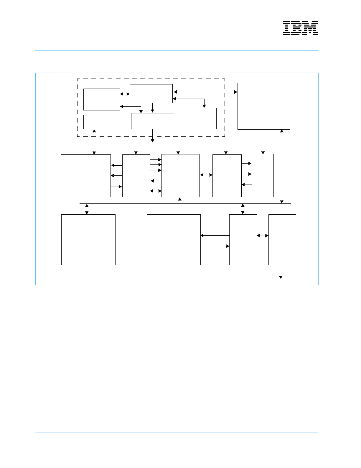
Figure 2-1 illustrates the architecture of the PPC750FX evaluation board. Subsequent sections discuss
aspects of Figure 2-1 in more detail.
2.1 Processor
The PPC750FX evaluation board is based upon the PPC750FX processor. See Section 1.1 PowerPC 750FX
RISC Microprocessor Features on page 13 for details. There are two PPC750FX processors on this board.
Figure 2-1. PPC750FX Board Architecture
CPU 0
Ethernet
NVRAM
Flash/SRAM
SDRAM
100/10
Serial Port
TAG/RISCWatch
Fast
x2
CPU 1
System
Memory
Controller
and PCI
Bridge
DDR
Interrupts
CPLD
4-Pin
PCI
Connector
Boot
Board Power
60x Bus
x2
ATX
Connector
Power
SEEPROM
SEEPROM
PCI
Bus

Evaluation Board Manual
PPC750FX Evaluation Board Preliminary
Board Design
Page 20 of 115
750FXebm_ch2.fm
une 10, 2003
2.2 Board Clocking
The clock architecture of the PPC750FX board is illustrated in Figure 2-2.
Figure 2-2. Clock Distribution on the PPC750FX Board
Clock
Generator
33.33MHz Osc Clock
Driver
External clock
MK74CB218 133MHz @ 2.5V
133MHz @ 2.5V
133MHz @ 3.3V
CPU 0
CPU 1
CPLD
System
Controller
MV64360
133MHz @ 3.3V
C9531AT
133MHz
Clock
Buffer
25MHz Osc
25MHz
CPLD
Clock
Multiplier
125MHz
Dual
Ethernet
PHY
25MHz
25MHz
ICS93V857
210 DDR SDRAM
BCM5222
Dual
UART
3.6864MHz Osc
STI6C2552
Clock
Driver
(see Note)
Note : Rework to the board is required to use the external oscillator input.
Table of contents
Other IBM Motherboard manuals


