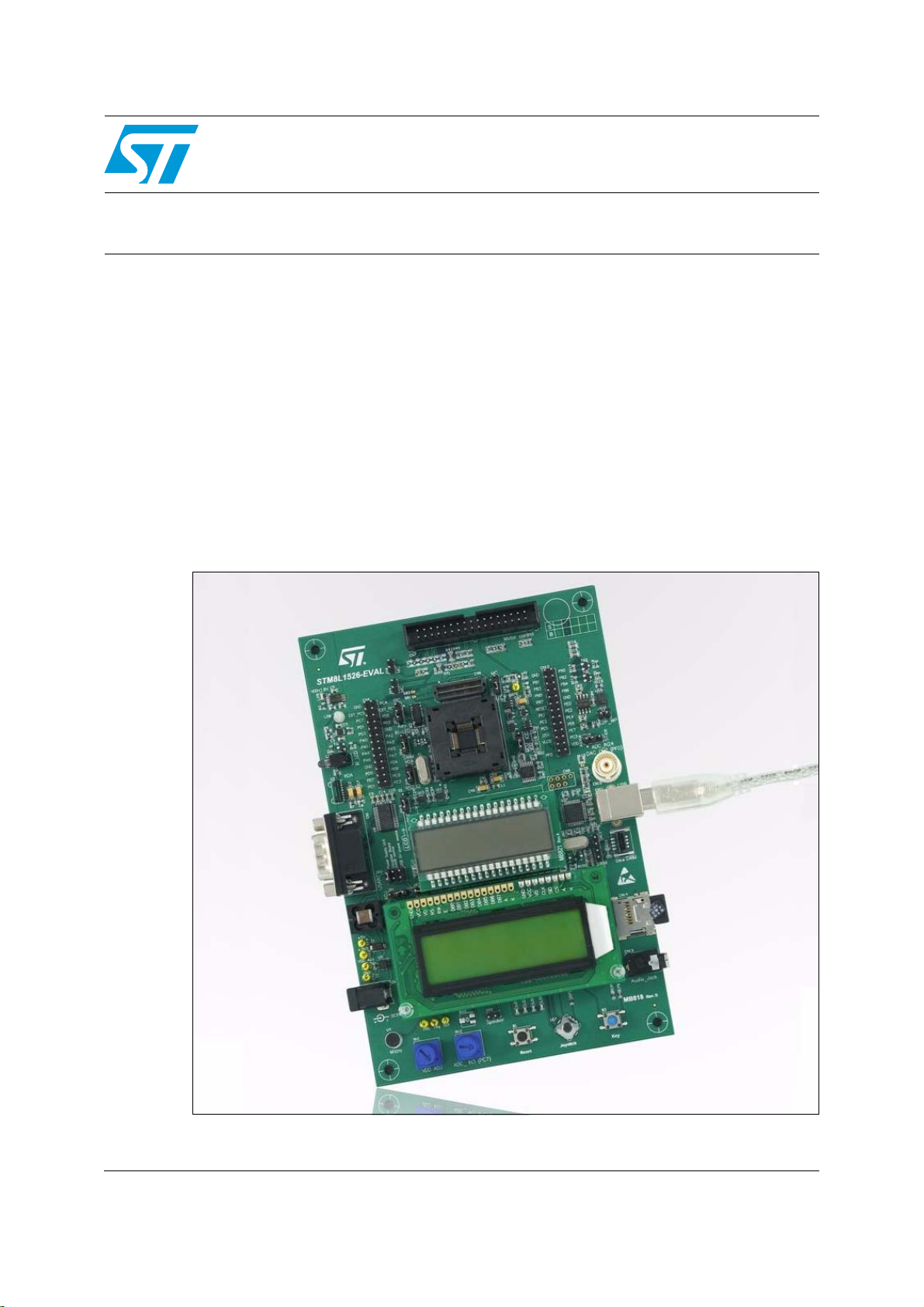
STM8L1526-EVAL Hardware layout and configuration
Doc ID 15437 Rev 1 9/46
To enable MCU power consumption measurement, JP11, JP3 and LCD glass module
should be re-configured as described in Table 1 and Table 2.
The LED LD8 is lit when the STM8L1526-EVAL evaluation board is powered by the 5 V
correctly, the LED LD9 is lit if the MCU is powered by a low voltage (VDD < 1.8 V).
Note: The AC220V to DC5V power adapter PSU-5V2A (recommended, can be ordered from ST, it
is not provided with board by default) or equivalent (polarity compatible with CN2) can be
used to power the STM8L1525-EVAL board via the power jack CN2 on the board.
To order the recommended power supply, use the order code PSU-5V2A.
2.2 Clock source
Two clock sources are available on the STM8L1526-EVAL for the STM8L152C6 and
embedded RTC.
●X2, 32 kHz crystal for embedded RTC
●X1, 16 MHz crystal with socket for the STM8L152C6 microcontroller, it can be removed
from the socket when the internal RC clock is used.
Note: I/O ports PA2 and PA3 can be used as GPIO on extension connector by closing solder
bridges SB1 and SB2 when crystal X1 is removed from it's socket.
Table 2. MCU power consumption measurement related jumpers
Jumper Description
JP3
The microphone output is connected to ADC of the STM8L152C6 when JP3 is closed.
Default setting: Fitted
For MCU power consumption measurement, JP3 must be kept open to avoid current
injection.
For motor control application, JP3 must be kept open to avoid conflict between the
speaker and motor control connector, CN7.
LCDglass
module The LCD glass module must be mounted on the "IO" position for MCU power
consumption measurement. Refer to Section 2.4: LCD glass module for details.
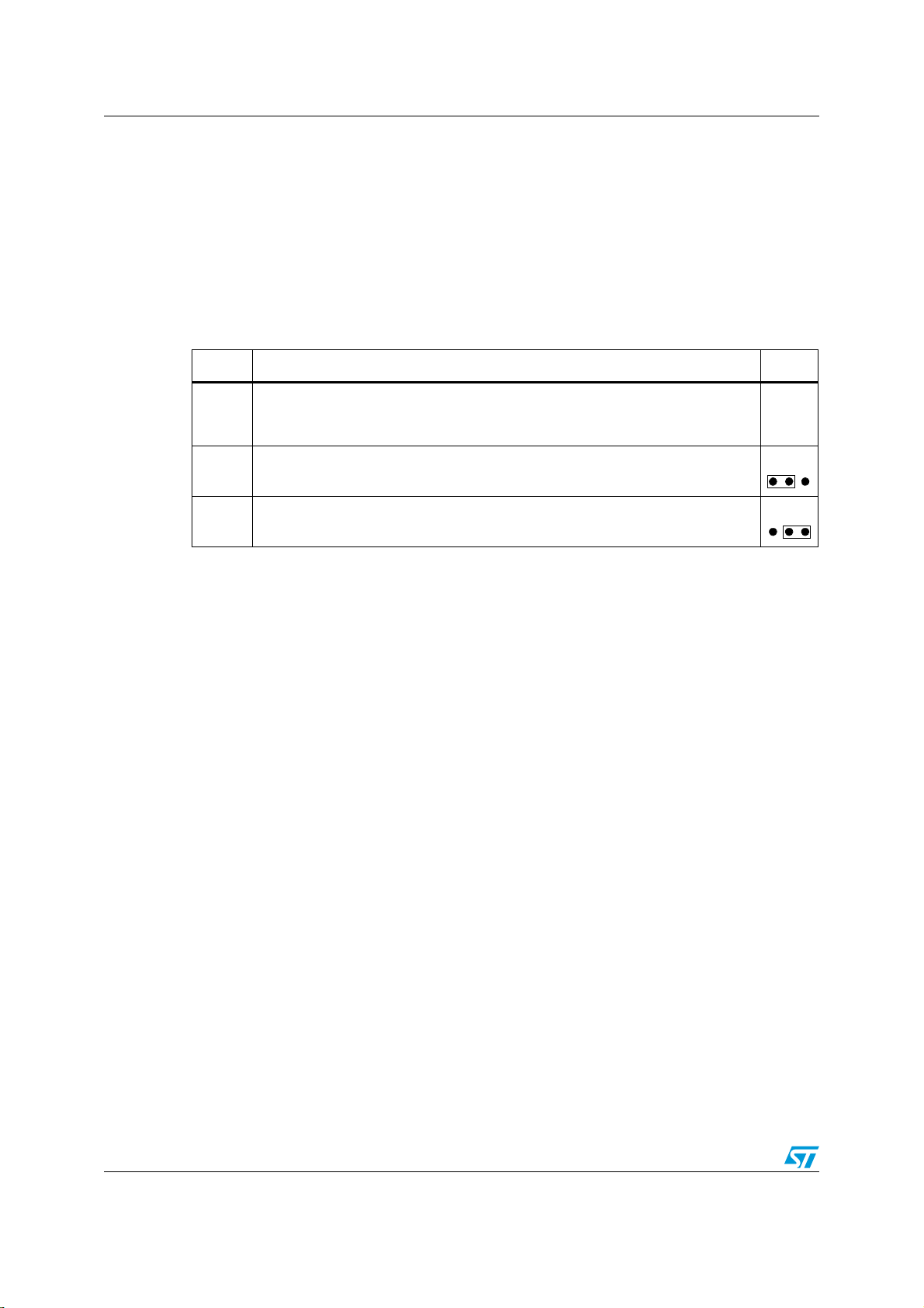
Table 3. 32 kHz crystal X2 related solder bridges
Solder bridge Description
SB3
PC5 is connected to 32 kHz crystal when SB3 is set as pad1 connected to pad2
(default setting).
PC5 is connected to STice connector CN8 and extension connector CN4 when SB3
is set as pad2 connected to pad3.
SB4
PC6 is connected to 32 kHz crystal when SB4 is set as pad2 connected to pad3
(default setting).
PC6 is connected to STice connector CN8 and extension connector CN4 when SB4
is set as pad1 connected to pad2.