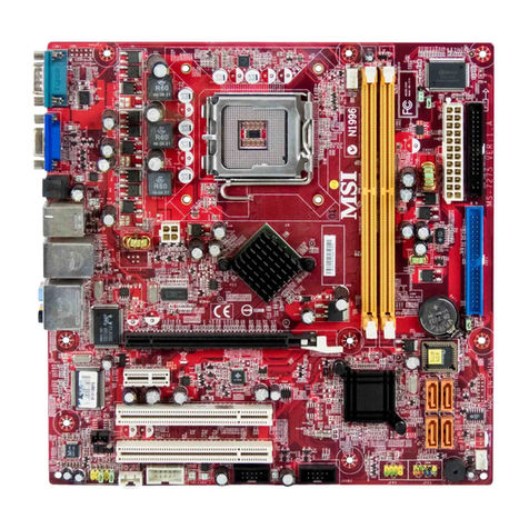
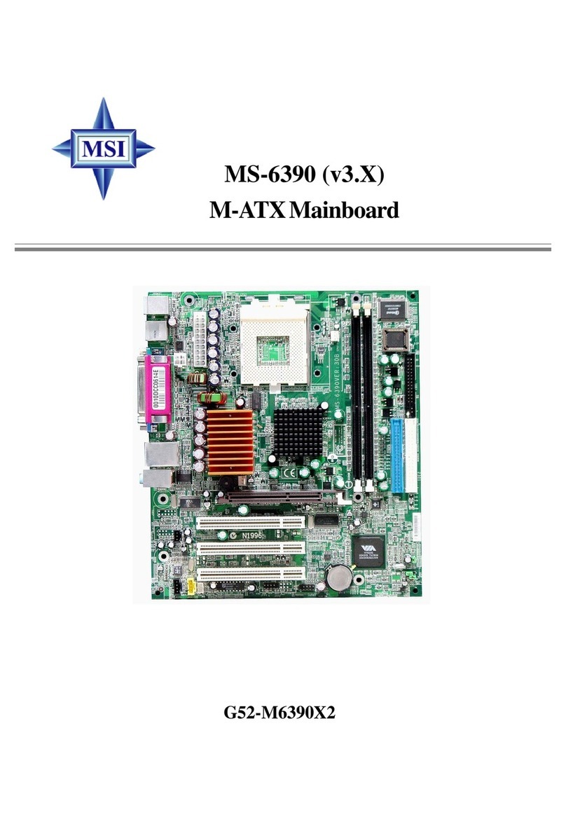
MSI MS-6104 User manual

Version 1.0
PENTIUM is a trademark of the Intel Corporation.
PS/2 is a trademark of the IBM Corporation.
1

Mainboard Name MS-6104
Manual Rev 1.0
BIOS Version W48X
Release Date June, 1996
FCC-B Radio Frequency Interference Statement
This equipment has been tested and found to comply with the limits for a
class B digital device, pursuant to part 15 of the FCC rules. These limits are
designed to provide reasonable protection against harmful interference
when the equipment is operated in a commercial environment. This
equipment generates, uses and can radiate radio frequency energy and, if
not installed and used in accordance with the instruction manual, may cause
harmful interference to radio communications. Operation of this equipment
in a residential area is likely to cause harmful interference, in which case
the user will be required to correct the interference at his own expense.
Notice 1
The changes or modifications not expressly approved by the party
responsible for compliance could void the user's authority to operate the
equipment.
Notice 2
Shielded interface cables and A.C. power cord, if any, must be used in
order to comply with the emission limits.
VOIR L NOTICE D'INST LL TION V NT DE R CCORDER
U RESE U.
2

Edition
June 1996
Copyright Notice
This manual is copyrighted. No guarantee is given as to the
correctness of its contents. We reserve the right to make changes
without notification.
Trademarks
All trademarks used in this manual are the property of their respective
owners.
3

Table of Contents
Chapter 1: Introduction
System Board Specifications ---------------------------------------- 1-1
System Board Layout ------------------------------------------------ 1-4
Chapter 2: Hardware Installation
System Clock Selection JC1--------------------- ------------------ 2-2
Flash ROM Selection JP3------------------------------------------- 2-3
Power Saving Switch Connector JG1----------------------------- 2-3
CMOS RAM Clear JP7---------------------------------------------- 2-4
System Memory Installation SIMM4 -SIMM1 ------------------- 2-4
DRAM Installation----------------------------------------------------
CPU Installation & Fan Power Connector -----------------------
2-6
2-7
Case Block Connector JFP------------------------------------------ 2-8
Power Supply Connector--------------------------------------------- 2-9
Keyboard Connector PS/2-KB or JMS1--------------------------
Mouse Connector JMS or PS/2 Style Mouse---------------------
2-
1
0
2-10
Serial Port Connectors COM1 & COM2-------------------------- 2-11
Parallel Port Connectors PRN--------------------------------------- 2-11
4

Floppy Disk Connector Floppy ------------------------------------ 2-12
Hard Disk Connector IDE1 , IDE2----------------------------- 2-12
IrDA Infrared Module Connector IRCON--------------------- 2-14
USB Connector USB (USB1,USB2) --------------------------- 2-15
Chapter 3: W RD BIOS SETUP (Version 4.51)
Entering Setup------------------------------------------------------- 3-1
Getting Help--------------------------------------------------------- 3-2
The Main Menu----------------------------------------------------- 3-3
Standard CMOS Setup ------------------------------------------- 3-6
BIOS Features Setup ---------------------------------------------- 3-9
Chipset Features Setup -------------------------------------------- 3-16
Power Management Setup----------------------------------------- 3-22
PNP/PCI Configuration Setup ------------------------------------ 3-29
Load BIOS/ Setup Defaults --------------------------------------- 3-32
Integrated Peripherals---------------------------------------------- 3-33
Supervisor/User Password Setting-------------------------------- 3-39
IDE HDD Auto Detection---------------------------------------- 3-40
5

CHAPTER 1 INTRODUCTION
Chapter 1
INTRODUCTION
The PCI P6 NA2 PCI/ISA system board is an ATX high-performance
personal comp ter system board based on the Penti mä Pro
microprocessor.
System Board Specifications
Po er Selection:
·ATX or PS/2 Power Selection
Hard are Installation:
·The system board provides “Pl g & Play” BIOS which detects
the peripheral devices and expansion cards of the board
a tomatically.
·The system board provides a Desktop Management Interface
(DMI) f nction which records yo r sytem board
specifications.
CPU:
·The system board s pports 150/166/180/200 MHz Intel Penti m
Pro CPUs.
Cache Memory:
·Internal Level 1 Cache: 8KB instr ction code and 8KB data
cache.
·Internal Level 2 Cache: 256KB/512KB(depending on CPU)
1 -
1

CHAPTER 1 INTRODUCTION
Chip Set:
·The system board tilizes the Intel Penti m Pro Chipset which
incl des SB82441FX (PMC) PCI bridge and memory controller, and
SB82442FX(DBX) Data B s Accelerator and SB82371(P11X3) PCI
to ISA Bridge.
Multi-I/O:
·The system board has a b ilt in Pl g and Play Winbond W83877
and M lti-I/O chipsets to s pport 2 high-speed serial ports, one
parallel port with ECP and EPP capabilities, and one floppy
drive.
Enhanced IDE Support:
·A PCI IDE controller and b ilt-in P11X3 s pports d al channels
and fo r hard drives.
IrDA and PS/2 support:
·This board s pports an infrared port connector for wireless
interface and a j mperless PS/2 mo se connector.
USB support:
·The system board s pports a two channel USB port connector.
AHA SCSI BIOS:
·This optional feat re s pports on-board an AHA AIC 7880 SCSI
controller.
Main Memory:
·S pports fo r memory banks sing fo r 72-pin SIMM sockets.
·Up to 512 Mbytes main memory.
·S pports Fast Page (FP) Mode, Extended Data O tp t (EDO)
Mode, and B rst Extended Data O tp t (BEDO) Mode
DRAM.
1 -
2

CHAPTER 1 INTRODUCTION
·S pports symmetric or asymmetric DRAM memory, 70ns or
faster.
·Provides ECC (Error Check F nction) F nction.
Slots:
·Fo r 32-bit PCI B s slots and fo r 16-bit ISA b s slots. One
shared slot that can be sed as ISA or PCI.
On-Board I/O:
·A 32-bit enhanced d al channel and 4 enhanced hard drives PCI IDE
controller, s pports fast-ATA2 PIO Mode 0-4 and b s Master
DMA Mode 2.
·One floppy disk drive controllers, two high-speed serial prots,
and one parrallel port with ECP or EPP capabilities.
·IrDA f nction.
·Optional SCSI controller.
·2 channel USB f nction.
Keyboard Connector:
·PS/2 keyboard interface and PS/2 Mo se interface.
·5X2-pin connector for PS/2 Keyboard and Mo se.
Dimensions
· ATX size: 30cm x 24.5cm x 6-layer PCB.
Mounting
·9 mo nting holes
1 -
3

CHAPTER 1 INTRODUCTION
1.2 System Board Layout
Figure 1-1
1 -
4

CHAPTER 2 HARDWARE INSTALLATION
Chapter 2
HARDWARE INSTALLATION
It is important to set jumpers correctly. Improper jumper setting
will cause system instability, destruction of components, and/or
system hang-up.
Step 1: Set the CPU US CLOCK and Core Frequency Ratio
(see “JC1 Jumper” section)
JC1 is used for CPU US CLOCK and bus to core
frequency ratio. Caution: If these jumpers aren’t set
correctly, it will cause the system to be unstable or system
hang-up, and it may reduce the life cycle of the CPU.
Step 2: Install CPU, VRM, DRAM, Expansion Card, and External
cables (see “Connectors” section)
Caution: All parts need to be set to avoid system board
malfunction.
Step 3: Turn Power on and setup IOS software (see “ IOS Setup”
section)
2 -
1

CHAPTER 2 HARDWARE INSTALLATION
Jumper Setting
This table is useful to conveniently locate information on specific
jumpers and connectors.
Jumper Setting/De cription Page
JC1 CPU Frequency Selection 2-2
JP3 Flash ROM Selection 2-3
JG1 Power Saving Switch Connector 2-3
JP1 CMOS RAM Clear 2-4
JFP Case Connector lock 2-7
PS/2-K Keyboard Connector 2-9
PS/2-MS PSII Mouse Connector 2-9
COM1 & COM2 Serial Port Connector 2-10
PRN Parallel Port Connector 2-10
FDD Floppy Disk Connector 2-11
IDE1 & IDE2 Hard Disk Connector 2-11
JFAN CPU Fan Connector 2-12
IRCON Infrared Module 2-12
CPU Frequency Selection: JC1
The CPU US CLOCK of the MS-6104 supports two frequencies:
60MHz (default) and 66MHz. Refer to the following figure for
jumper location and settings.
2 -
2

CHAPTER 2 HARDWARE INSTALLATION
JC1 SETTINGS
Fla h ROM Selection: JP3
Jumper JP3 sets the mainboard to be used with either +12V or +5V
Flash ROM.
2 -
3

CHAPTER 2 HARDWARE INSTALLATION
Power Saving Switch: JG1
Attaching a power saving switch to this connector will allow the
system into sleep mode whenever this switch is pressed.
CMOS RAM Clear: JP1
The system board configuration is stored in CMOS RAM. If you
need to clear the system board configuration do the following:
1. Turn power off.
2. Short jumper JP1.
3. Turn power on.
4. Enter the IOS setup
to re-setup the IOS.
5. Reboot the system.
2 -
4

CHAPTER 2 HARDWARE INSTALLATION
Note: Some CMOS RAMs require a different procedure:
1. Short jumper JP1.
2. urn on system
3. urn off the system
4. Remove JP1 jumper.
5. Turn on power again.
6. Reset IOS.
Sy tem Memory In tallation: SIMM1-SIMM4
The system board provides four 72-pin SIMM sockets which are
numbered from SIMM1 to SIMM4. The system board supports
memory sizes from 8M to 512M using 4M , 8M , 16M ,
32M , 64M , and 128M DRAM modules. It supports both Fast
Page Mode (FP), Extended Data Output Mode (EDO), and urst
Extended Data Output Mode ( EDO), with symmetric or
asymmetric row/colum address.
DRAM Population Rule
In order to create a memory array, certain rules must be followed.
The following set of rules allows for optimum configuration.
1. DRAM modules must be populated in pairs; the
memory array is 64-or-72-bits wide. (64-bit
modules are no parity.)
2 -
5

CHAPTER 2 HARDWARE INSTALLATION
2. DRAM modules can be populated in any order
(i.e. SIMM1/2 does not have to be populated
before SIMM3/4 are used.)
3. DRAM module pairs need to be populated with
the same densities...single or double. For
example, SIMM1/2 sockets must be populated
with identical densities. However SIMM3/4
sockets can be populated with different densities
than SIMM socket pair 1/2. In addition,
asymetric DRAMs of the same type should be
used in a whole row.
4. EDO, EDO, FP modes can be mixed in the
memory array. However only one type should be
used per SIMM socket pair. For example:
SIMM sockets 1 & 2 can be populated with EDO
while SIMM sockets 3 & 4 can be populated with
FP mode type DRAM.
5. The DRAM timing which provides the DRAM
speed grade control for the entire memory array
must be programmed to use the timing of the
slowest DRAM that is currently installed.
Note: o use the ECC (Error Code Correct) function, a SIMM module with
parity support must be used. At this time you can turn on the ECC function
in the BIOS setup.
Note: Before using DRAM modules, make sure that that the modules used
is the same as in the above chart.
DRAM Memory In tallation
2 -
6

CHAPTER 2 HARDWARE INSTALLATION
1. Check to see which side of the plastic safety tab is on the slot
before installing.
2. Line up the notch of the module against the slot.
3. Press the module firmly into place at a 45 degree angle.
4. Carefully press down on the top edge of the module to set it in
the SIMM slot.
5. The plastic guides should go through the two holes on the sides
and the metal clips should snap on the other side. If it doesn’t
slide in easily, take it out and try again.
6. To release module, squeeze both metal clips outwards and rock
the module out of the metal clips.
CPU In tallation
Open Socket 8 by pulling the lever away from the socket then
upwards at a 90 degree right angle. Insert the CPU according to the
orientation as shown. IF it does not fall in easily then try a different
direction because the pin configuration only fits one way as opposed
to earlier CPUs. Make sure that the CPU is well seated and close to
the lever. See following figure:
2 -
7

CHAPTER 2 HARDWARE INSTALLATION
Ca e Block Connector : JFP
The Turbo LED, Hardware Reset, Key lock, Power LED, Power
Saving LED, Speaker,and HDD LED all connect to the JFP
connector block as below.
2 -
8

CHAPTER 2 HARDWARE INSTALLATION
Note : he hardware urbo switch is not functional. But the urbo
LED can be controled by software urbo/Deturbo.
Power Supply Connector
The power supply connector is a twelve-pin male connector (J1) or a
2X10-pin ATX connector (J3). Dual connectors from the power
supply can fit in only one direction. Make sure to attach the
2 -
9

CHAPTER 2 HARDWARE INSTALLATION
connector with the two black wires at the center as shown in the
diagram below.
12-pin Connector Pin Description
Pin Description Pin Description
1 Power Good
2 +5V DC
3 +12V DC
4 -12V DC
5 Ground
7 Ground
8 Ground
9 -5V DC
10 +5V DC
11 +5V DC
2 -
10

CHAPTER 2 HARDWARE INSTALLATION
6 Ground 12 +5V DC
2X10-Pin Connector Pin De cription
Pin De cription Pin De cription
1 3.3V 11 3.3V
2 3.3V 12 -12V
3 GROUND 13 GROUND
4 5V 14 PS-ON
5 GROUND 15 GROUND
6 5V 16 GROUND
7 GROUND 17 GROUND
8 PW-OK 18 -5V
9 5VSV 19 5V
10 12V 20 5V
Keyboard Connector: PS/2-KB, or JMS1
Choose either PS/2-K or JMS1 as a keyboard connector. The
system board provides a standard five-pin female DIN connector for
attaching a keyboard. You can plug a keyboard cable directly into
this connector.
2 -
11
Table of contents
Other MSI Motherboard manuals

MSI
MSI Z370I GAMING PRO CARBON AC User manual

MSI
MSI MS7797 User manual

MSI
MSI H270 GAMING PRO CARBON User manual

MSI
MSI K9NGM3 Series User manual

MSI
MSI LPX SI15 User manual

MSI
MSI MEG Z690 GODLIKE User manual

MSI
MSI MS-S3361 User manual

MSI
MSI MAG B460 TOMAHAWK User manual

MSI
MSI MAG B660M MORTAR WIFI DDR4 User manual

MSI
MSI MS-6198 User manual

MSI
MSI P45 Platinum Series User manual

MSI
MSI B760 GAMING PLUS WIFI User manual

MSI
MSI 915PM User manual

MSI
MSI A88X-G41 PC Mate User manual

MSI
MSI MPG Z590 GAMING CARBON WIFI User manual

MSI
MSI MAG B660M MORTAR WIFI DDR4 User manual

MSI
MSI H610TI-S03 User manual

MSI
MSI Z87M GAMING User manual

MSI
MSI B760M PROJECT ZERO User manual

MSI
MSI MS-6135 User manual