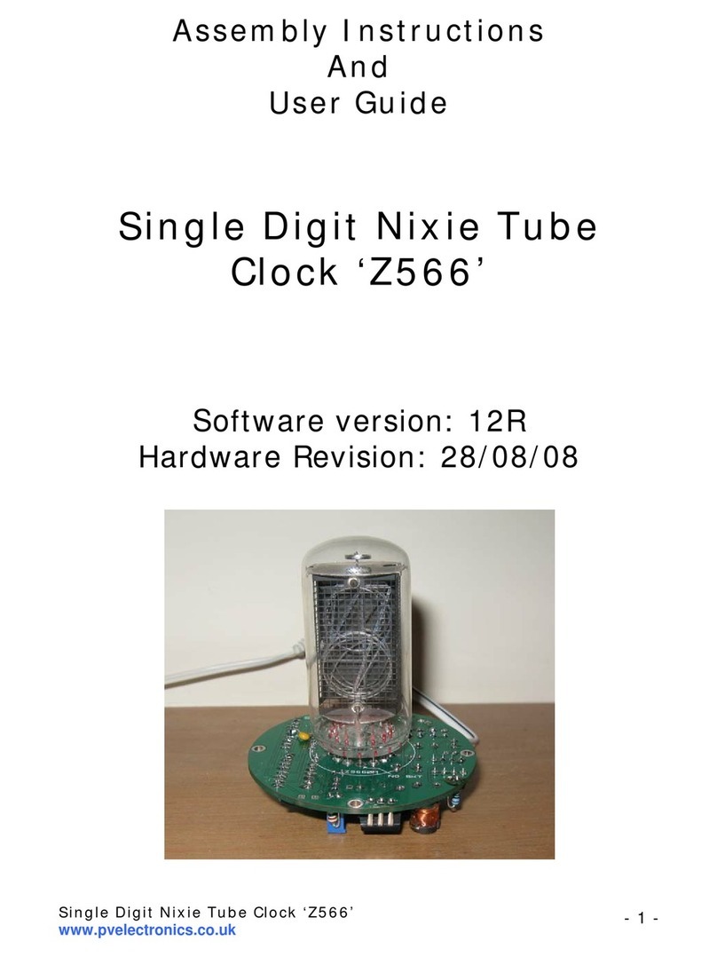
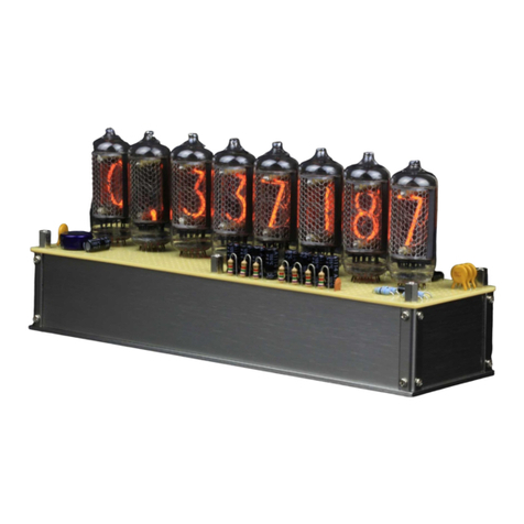
Nixie UNIVERSAL TUBE CLOCK KIT Installation instructions

UNIVERSAL NIXIE TUBE CLOCK KIT
Assembly instruction and user manual
Bring to your home a piece of history with The Vintage Nixie Clock and its Cold War era
components. The clock will give a cosiness and a uniqueness for your house.

2
Introduction
This parts kit intended for an electronics hobbyists that want to make a Nixie clock and do not want
go deep to complicated clock control electronics and software. This instruction step-by-step assists
you to assemble the clock.
The kit consists all necessary electronics parts (excluding Nixie tubes and power adapter) and a
microcontroller with pre-programmed an application software.
The main features of the clock
Hours, Minutes and Seconds display
12 or 24 hour operation modes
Time accuracy is provided by built-in RTC (Real Time Clock) based on extremely precise
DS3231 module with temperature compensation and backup with CR2032 battery
Programmable leading zero blanking
Date display in either DD/MM/YY or MM/DD/YY format
Alarm
Simple time setting using three buttons
Standard, crossfade and scrollback display modes
“Slot Machine” Cathode poisoning prevention routine
Programmable Blue LED tube lighting
Not AC frequency dependent –works in all countries
Auto increase of adjusting value for quick time setting
Neon colon indicators blinking at 1 Hz
Tubes are driven in high frequency dynamical indication and provide service for many years

3
Safety precautions
The clock printed circuit board (PCB) includes a High Voltage source that powers the Nixie tubes. It
output voltage can reach 180 Volts DC. The voltage generated by this source can give a potentially
LETHAL ELECTRIC SHOCK. When PCB is powered its contacts shall be not touched by hands or non-
isolated tools (non-isolated tweezers for example).
Required experience
This product is supplied as a kit of parts, intended only for suitably qualified electronic hobbyists, who
are suitably qualified and experienced in electronics assembly and electronics components proper
soldering, and are familiar with safe procedures for working with high voltage and its potentially
danger.
Assembly and testing of the clock from this kit should be attempted by competent persons only, or
under supervision of someone fully experienced in this field.
Correct component placement is critical. A few minutes spent checking placement and orientation
prior to soldering will save hours of mistakes search and rework later.
REMEMBER: A properly placed components and carefully soldered PC board will perform well for
years, a hastily assembled board will cause ongoing clock problems and failures.
The most important skill for our kit assembly is an electronic components soldering. If you have not
an experience enough, next site with Basic Soldering Guide will be useful for you:
https://learn.sparkfun.com/tutorials/how-to-solder-through-hole-soldering
Tools and materials required for assembly
Screwdriver
Angled tweezers with thin noses
Long nose pliers for tube leads bonding
Side cutting pliers to trim the excess component leads after soldering
Electronics grade solder 0.5-1mm thickness that contains cores of "flux" which helps the
molten solder to flow more easily over the joint
De-soldering wick or pump may be useful if you accidentally create solder bridges between
adjacent solder joints or improper solder any component
Soldering iron with small a “tinned” tip
Multi-meter for voltage measurements and for identifying the resistors
Magnifying glass.
4
The clock kit does not include next components
A power adapter. Output voltage 12V DC, output current ~1A. Output end plug –5.5 x 2.1mm,
centre positive. It is cheaper to buy such power adapter in your local electronics shop because
it will be equipped by necessary grid plug. You may have similar power adapter in your house
also because such type power adapters are popular and widely use.
The KIT consists electronics components necessary for a clock assembly only. Nixie tubes need
to purchase separately. This KIT can work with many nixie tube models. Tested with In-8, In-8-
2, In-18, In-12, In-14, In-16, In-1, z573m. Controller does not support biquinary type nixie
tubes.
The KIT does not consist the case of the clock also.
Wires and nixie tubes sockets are not included.

5
Parts list
Component designation
Component description
RESISTORS
R1
1kΩ, 0.25W
R2
470kΩ, 0.25W
R3
3.3kΩ, 0.25W
R4
0.5Ω, 0.5W
R5, R6, R7, R8, R9, R10, R11, R14, R17, R18
R19, R20
10kΩ, 0.25W
R12
330Ω, 0.25W
R15, R16
270kΩ, 0.25W
R21
1K, 0.1W (Potentiometer)
CAPACITORS
C5
2.2uF, 250V, Electrolytic
C2, C4, C6, C7
0.1uF, Ceramic
C3
2.2nF, Ceramic
C1
220uF, 25V, Electrolytic
TRANSISTORS

6
Q1
BC557
Q2
IRF840, MOSFET
Q3, Q4, Q5, Q7
BC547
Q6
MPSA42
OK1-OK6
EL817, Optocoupler
DIODES
D1
1N4004
D2
1N914
D3
UF4004
LED1-LED6
LED, 3mm
INTEGRATED CIRCUITS
U1
LM7805
U2
MC34063
U3
K155ID1
U4
ATMEGA328P-PU
U5
DS3231
MISCELLANEOUS
PCB
Nixie Clock PCB
BAT_1
CR2032 Battery socket
Battery
3V CR2032
DB1, DB2
Neon bulb
FUSE
0.5A
L1
330uH, 1A Inductor
S1 - S3
Buttons
U3 Socket
16pin socket
U4 Socket
28pin socket
Power socket (JP1)
5.5mm x 2.1mm
Speaker (SP1)
Active alarm buzzer
PCB Spacers
4 PCB spacers
Screws
4 Screws 3mm
J2, J3, J4, J5, DB1, DB2
Pin strips

7
Components review
Resistors
1kΩ (R1)
10kΩ (R5, R6, R7, R8, R9,
R10, R11, R14, R17, R18, R19, R20)
470kΩ (R2)
0.5Ω (R4)
3.3kΩ (R3)
330Ω (R12)
270kΩ (R16, R17)
1k (R21)
NOTES:
Components actual view can differ due to different manufacturers.
If an inscription or color bar coding of the component is small, it is necessary to use the
magnifying glass.

8
The resistors used in the kit are marked with four coloured bands to identify the value. Bands 1 and 2
identify the first two digits, band 3 is the Multiplier and band 4 is the tolerance.
The first, second and third coloured bands on the resistors indicate the resistance using a colour code.
This table indicates how to convert each colour to its numerical equivalent. Gold band means 5%
tolerance.
To read a resistor code, first locate the gold band and read the colours in order from the other end.
(All resistors in this kit have a gold band indicating 5% tolerance.) The first two bands indicate digits in
the resistance; the third band (called the multiplier) indicates the number of zeroes to be added to
the digits to obtain the resistance. However, it is sometimes unclear in which direction the bands
should be read. Therefore, we recommend that the resistors will be identified with a multimeter.
Use the resistor code to identify and sort all of the resistors. One good way to keep them sorted is to
tape one end to a piece of paper and write the resistance and component number (R1, R2, etc.). Once
you have identified and sorted all of the resistors, you are ready to solder them to the PCB. To
prepare a resistor for insertion into the board, bend the two leads so that they form a right angle to
the resistor body.
Capacitors
0.1uF (Code 104), (C2, C4, C6, C7)
2.2nF (Code 222), (C3)
220uF 25V, (C1)
Band colour
Numerical
equivalent
Band colour
Numerical
equivalent
black
0
green
5
brown
1
blue
6
red
2
violet
7
orange
3
grey
8
yellow
4
white
9

10
IRF840, MOSFET, (Q2)
EL817, (OK1-OK6)
Diodes
1N4004 (D1)
UF4004 (D3)
1N914 (D2)
LED, 3mm

11
Integrated Circuits
LM7805 (U1)
MC34063 (U2)
K155ИД1 (U3)
ATMEGA328P-PU (U4)
DS3231 (U5)

12
Miscellaneous
CR2032 Battery socket (BAT_1)
Battery
Neon bulb (DB1, DB2)
Fuse
330uH, 1A Inductor (L1)

13
Button (S1-S3)
16 pin socket
28 pin socket
Power socket (5.5mm x 2.1mm)
Speaker
PCB Spacers
3mm screw

14
Packing Sheet
Component description
Quantity, pcs
RESISTORS
1kΩ, 0.25W
1
470kΩ, 0.25W
1
3.3kΩ, 0.25W
1
0.5Ω, 0.5W
1
10kΩ, 0.25W
12
330Ω, 0.25W
1
270kΩ, 0.25W
2
1k (Potentiometer)
1
CAPACITORS
2.2uF, 250V, Electrolytic
1
220uF, 25V, Electrolytic
1
0.1uF, Ceramic
4
2.2nF, Ceramic
1
TRANSISTORS
BC557
1
IRF840, MOSFET
1
BC547
4
MPSA42
1
EL817, Optocoupler
6
DIODES
1N4004
1
1N914
1
UF4004
1
LED 3mm
6
INTEGRATED CIRCUITS
LM7805
1
MC34063
1
K155ID1
1
ATMEGA328P-PU
1
DS3231
1
MISCELLANEOUS
Nixie Clock PCB
1
CR2032 Battery socket
1
CR2032 Battery
1
Neon bulb
2
330uH, 1A Inductor
1
Buttons
3
16 pin socket
1
28 pin socket
1
Power socket (5.5mm x 2.1mm)
1
Speaker
1
PCB spacers
4
Screws
4
Fuse
1
Pin Strips (Male)
30
Pin Strips (Female)
30

15
PCB assembly sequence
1. Screwing PCB spacers to PCB by screws
Spacers lift the PCB over table surface. It will be more convenient to install and to solder components
to the PCB. These spacers can use for fixing an assembled clock in applicable casing also.
NOTES:
This instruction contents high definition pictures. If anywhere is uncertainty, PCB view
can magnify and an interested component may to view in details.
The side of the board that has printed component marking is the “component side”. This
means that components must mount by inserting them down from the printed side.
Make sure that the components mount on the proper side of the PCB!
Prior to beginning an assembly, make sure to have a well-lighted, well-ventilated
workplace. Make sure that all of the electronic assembly tools are available.

16
2. Low Voltage Power source components preparation for insertion into the board
and soldering order
U1
LM7805
C1
220uF, 25V, Electrolytic
C7
0.1uF, Ceramic
D1
1N4004
FUSE
FUSE 0.5A
Power socket
5.5mm x 2.1mm PCB DC Jack
2.1. Bend U1 integrated circuit leads.
2.2. Bend the two leads of the fuse and diode D1 so that they form a right angle to the component
body.
2.3. To install, place the leads of the component through the appropriate holes and press the
component down against the component side of the PCB.
2.3.1. The small-value ceramic capacitor (C7) may be installed in either orientation, but the larger-
value cylindrical capacitor (C1) must be installed with the proper polarity. The polarity is indicated on
the PCB by a “+” sign near one end of the capacitor location. The polarity is indicated on the body of
the capacitor with a stripe with a minus (-) sign located on the negative side of the capacitor. In
addition, the shorter lead is the negative lead.

17
2.3.2. Either lead of the fuse may be inserted in either hole its location.
2.3.3. Turn the board over while holding the relevant component in position and bend the leads
slightly outward to hold the component in place. Solder the leads to the contact and trim the excess
lead wire above the solder joint.
NOTES:
To make sure that capacitor C1 and diode D1 polarity is not mistaken.
To make sure that integrated circuit U1 (LM7805) is not mistaken with transistor Q2
(IRF840) and diode D1 (1N4004) is not mistaken with diode D3 (UF4004) because they look
like similar.

18
3. High voltage generator components preparation for insertion into the board and
soldering order
U2
MC34063
Q1
BC557
Q2
IRF840
D3
UF4004
D2
1N914
L1
Inductor 330uH
C5
2.2uF, 250V
C2, C4
0.1uF
C3
2.2nF
R4
0.5Ω 0.5W
R1
1k
R3
3.3k
R2
470k
R21
1k (Potentiometer)
3.1. All resistors (except R4) leads bend in accordance with this picture
that each resistor place on board surface will be minimal.
3.2. Repeat actions pointed in items 2.3, 2.3.1 and 2.3.3 for proper components insertion into the PCB
and soldering.

19
4. Low and High Voltage sources operability test
After Low and High Voltage sources components assembly it is necessary to check relevant source
proper operability.
4.1. Select multi-meter DC 200 V measuring range.
4.2. Identify the test ground (GND), 5V and HV test points as shown below.
4.3. Plug in the power supply, and then test HV source operability using a multi-meter in DC voltmeter
mode. Touch the black probe on the GND test point and the red probe on the HV test point. The
voltage should measure between 140 and 180 Volts. When PCB is powered its HV source contacts
shall be not touched by hands or non-isolated tools (non-isolated tweezers for example). If not,
disconnect power and remember that the HV source output could still hold charge at 165-175 V.
Check all relevant joints quality and polarity.
Do not continue with the next test until the error in HV source exists.
NOTES:
Turn the potentiometer to adjust the voltage to approximately 165V. A potentiometer is
needed to change the brightness of the nixie tube.

20
4.4. Test low voltage (LV) source operability. Touch the black probe on the GND test point and the red
probe on the 5V test point. The voltage should measure between 4.8 and 5.2 Volts. If not, disconnect
power and check all relevant joints quality and polarity.
Do not continue with the assembly until the error will be corrected.
4.5. Once the last test of LV source is completed, disconnect the power.
5. Microcontroller circuit components assembly
U4
Atmega328P-PU
R11
10kΩ
U4 Socket
28 pin socket
5.1. Take the resistor R11 and bend it, like pointed in item 3.1. Insert resistor into the board holes
marked as R11 and solder it leads.
5.2. Insert U4 socket and solder it leads.
This manual suits for next models
1
Table of contents
Other Nixie Clock manuals
Popular Clock manuals by other brands

La Crosse Technology
La Crosse Technology 404-1210S instruction manual

Oregon Scientific
Oregon Scientific BAR623PA user manual

La Crosse Technology
La Crosse Technology 513-1417H-AL Faqs

American Time
American Time PGE441RFE-W Quick start installation guide

LA CROSSE CLOCK
LA CROSSE CLOCK BBB85456 instruction manual

Bogen
Bogen BCBD 2000-SERIES instructions

Valentin Elektronik
Valentin Elektronik C 210 Series installation instructions

ABB
ABB twa-1 user manual

La Crosse Technology
La Crosse Technology BBB84022 instruction manual

Clas Ohlson
Clas Ohlson IP22B manual

SG Electronics
SG Electronics SGCLK046 user manual

Infineon
Infineon TRAVEO T2G family CYT4D Series manual