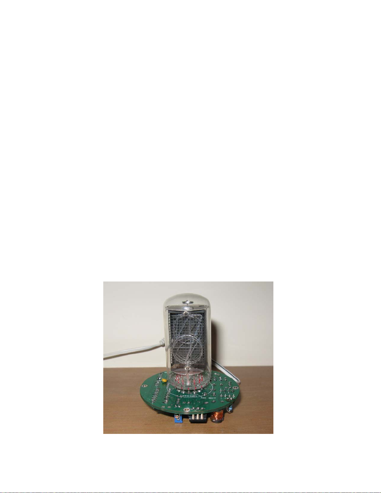
Single Digit Nixie Tube Clock ‘Z566’
www.pvelectronics.co.uk - 4 -
2. TOOLS AND EQUIPMENT REQUIRED
2.1 Tools required to assemble the PCB
The following tools will be required to assemble the PCB:
-Soldering iron with a small tip (1-2 mm)
-Wire cutters (TIP: A small pair of nail clippers works very well
for this function)
-Wire strippers (TIP: A small pair of scissors is quite suitable)
-Multimeter
-Small flat screwdriver for adjusting the high voltage supply
2.2 Materials you will need
Solder – lead / tin solder is preferred. Lead – free solder, as now
required to be used in commercial products in Europe, has a much
higher melting point and can be very hard to work with.
Desoldering wick (braid) can be useful if you accidentally create
solder bridges between adjacent solder joints.
2.3 Other items you will need
The clock kit does not include a power adapter. This is because the
kit is sold to many countries around the world, each with very
different household mains outlet socket types. It is more efficient
for the user to buy a suitable adapter locally. This saves shipping a
heavy adapter with the kit, and also the extra costs of managing
stocks of many varied power adapters.
The type of power adapter can be obtained at very low cost. The
following type of adapter should be obtained and used with the kit:
Mains AC to AC adapter (This is important, as the AC signal is
needed for the timebase)
Output 9-12V AC
Minimum power output capability of 250 mA
Output plug: 2.1mm pin
A suitable adapter is shown in figure 1 below:
Figure 1