CONFIDENTIAL 9 (25)
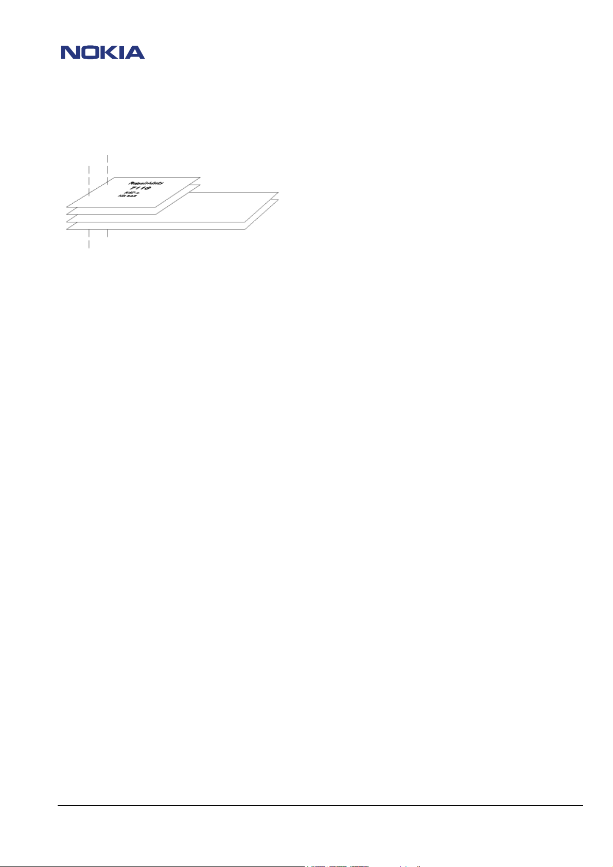
NPE-4 6310/NPL-1 6310i Repairhints
Customer Care Europe & Africa Version 1.0 Approved
SCCE Training Group Date 15.08.2002
©NMP 2002 Checked by:
SCCE Training Group
Approved by:
SCCE
Drop calls
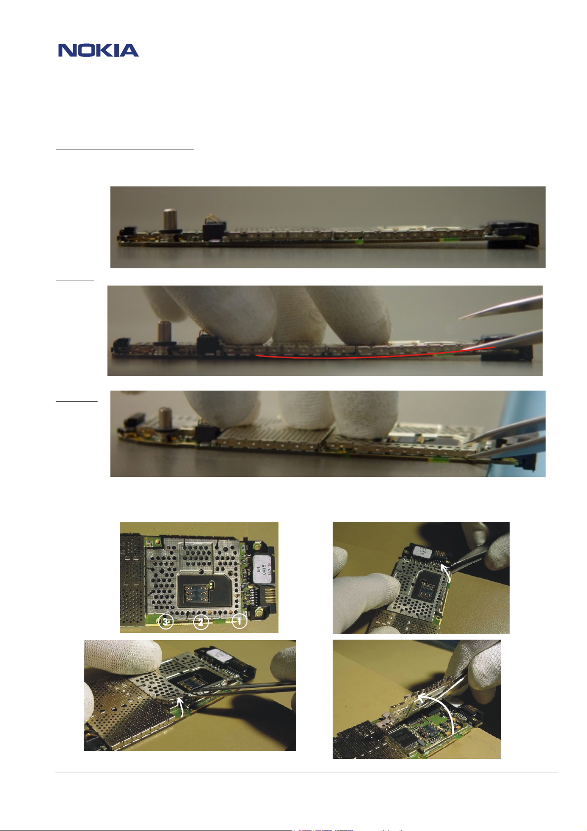
Disassemble the NPE-4 and the RF- shield, then connect the PWB to the MJS-40 jig.
Insert a SIMcard and connect the coaxial cable to the tester (e.g. CMD/Wavetec). Now start a call.
If the call is established, check the analyzer display from tester (e.g. CMD/Wavetec) shows a frequency error.
If fault does not appear or appears intermittently only, press on 26MHz oscillator G740 with non-metallic item.
If the frequency error appears or increases in this case, probably the 26MHz circuit is faulty.
Open the Phoenix menu Testing/ RF controls and activate local mode RX GSM900
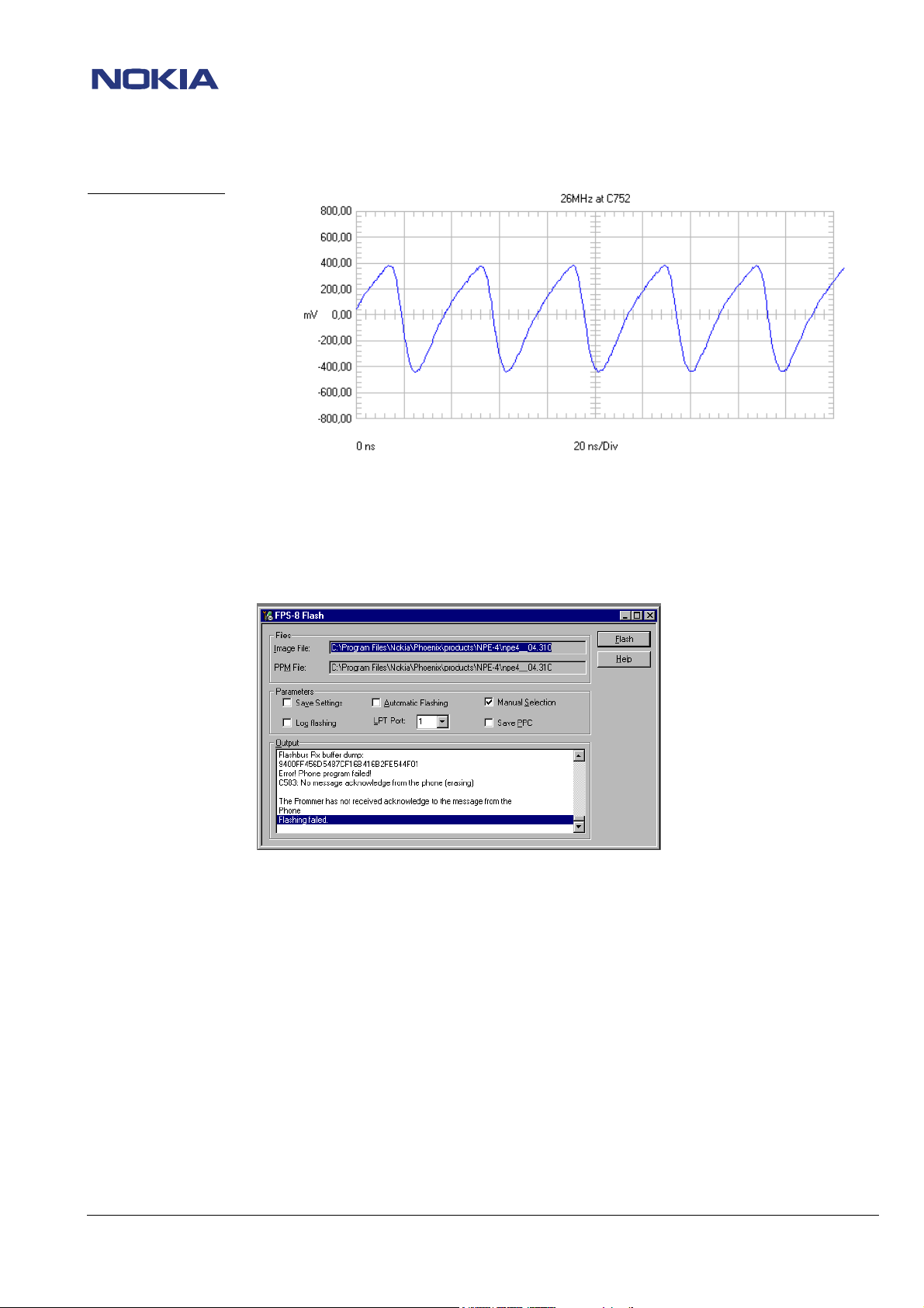
Check 26MHz +/- 100Hz between C752 and R752 with spectrum analyzer and active frequency counter (See picture below)
If the frequency drift is higher than +/ - 100Hz, check VR3 (VCC) = 2.8 VDC at R740.- If not ok, check UEM D200.
Check AFC (around 1.3 VDC) at G740. Check also if VR3 (VCC = 2.8 VDC) is ok with an Oscilloscope.- If not ok, check UEM D200
If both voltages are ok but the frequency drift is higher than +/ - 100Hz and the fault is getting stronger when pressing the top of
the 26MHz oscillator G740, change the faulty component.
No service
Set phone to local mode with Phoenix
Open menu Maintenance/Tuning/RX Calibration
Check RX calibration in GSM/PCN. If not ok, refer to chapter No Service/No RX
If RX calibration is ok, open menu Maintenance/Tuning/TX power
Check TX power in GSM/PCN. If not ok, refer to chapter No Service/No TX
If TX power is ok, insert Test-SIM and set phone to normal mode.
Start a Test call If not ok, make a SW update and try connecting again.
If the fault persists after SW update, rewrite IMEI and SIMLock settings.
Note! Rewrite SIMlock and IMEI data by use of NOKIA SECURITY PASSWORD and make a SW-update again, if the
procedure is permitted to you. (See General SB–037)
If the connection is established, check with tester (e.g. CMD/Wavetec) if any errors appears on display (e.g. frequency error).
If a frequency error appears, refer to chapter Drop calls.