Nokia NPL-3 Series Guide

Customer Care Solutions
NPL-3 Series Transceivers
Issue 1 3/03 ãNokia Corporation
Troubleshooting Instructions

NPL-3 Company confidential
Troubleshooting Instructions CCS Technical Documentation
Page 2 ãNokia Corporation. Issue 1 3/03
Table of Contents
Page No
RF Troubleshooting .......................................................................................................3
Introduction to RF troubleshooting .............................................................................3
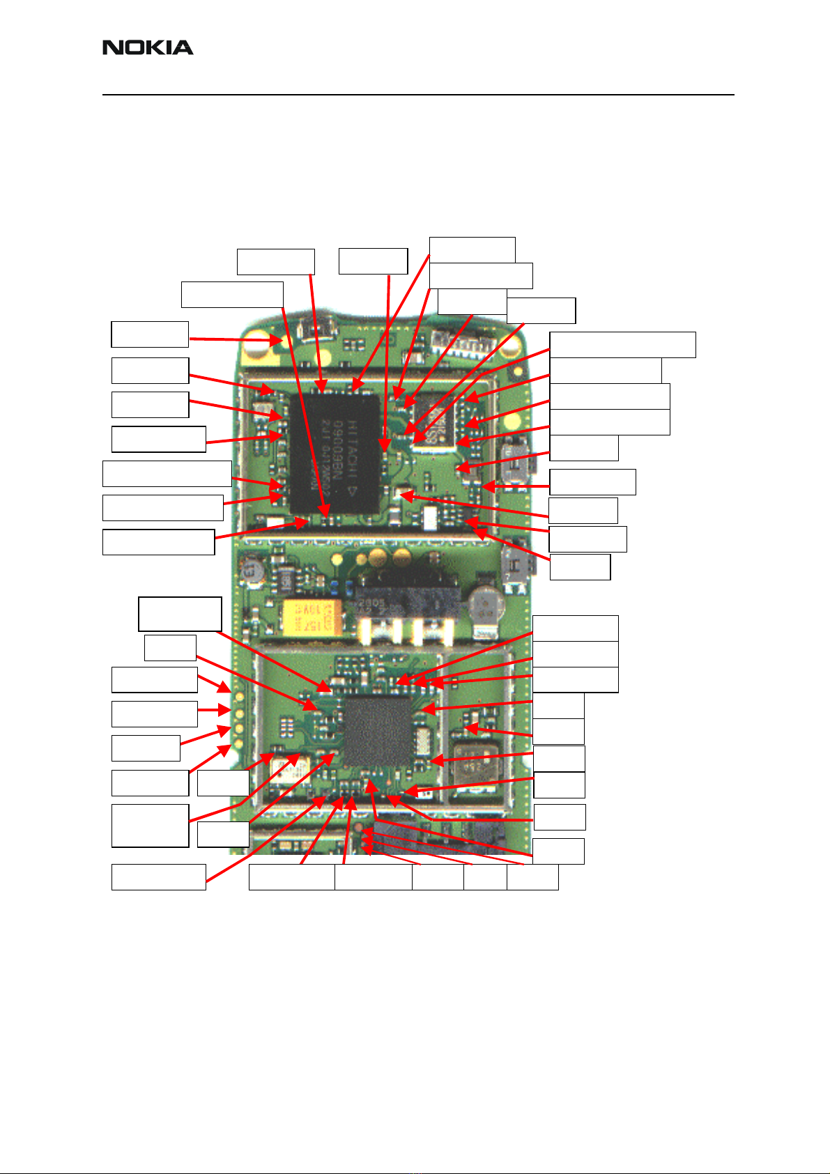
RF Key component placement .....................................................................................4
RF Measurement points ...............................................................................................5
GSM850, GSM1800 & GSM1900 Transmitter .............................................................6
General instructions for Tx troubleshooting .............................................................6
Transmitter troubleshooting diagram ........................................................................8
Pictures of transmitter signals .................................................................................11
Additional information for EDGE troubleshooting .....................................................13
EDGE mode troubleshooting differs slightly from basic GSM troubleshooting ....13
Pictures of EDGE transmitter signals ......................................................................17
GSM850, GSM1800 and GSM1900 Receiver .............................................................21
General instructions for Rx troubleshooting ...........................................................21
Troubleshooting diagram for GSM850 receiver .....................................................25
Troubleshooting diagram for GSM1800 receiver ...................................................26
Troubleshooting diagram for GSM1900 receiver ...................................................27
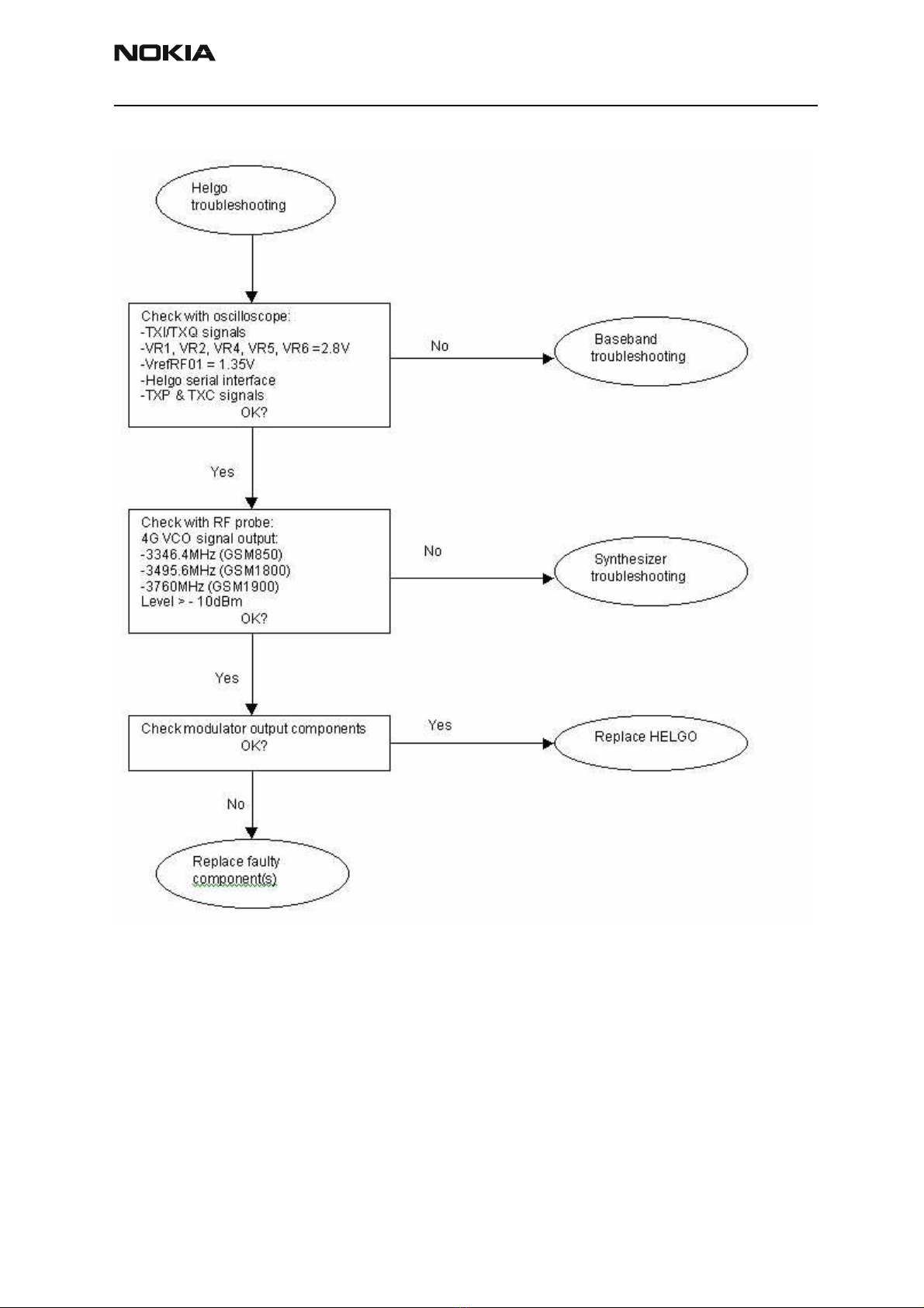
Synthesizer ...................................................................................................................28
General instructions for synthesizer troubleshooting ..............................................28
Pictures of synthesizer signals .................................................................................30
Baseband troubleshooting ............................................................................................32
Main Troubleshooting Diagram ................................................................................33
Phone is dead .............................................................................................................34
Flash Programming Fault ..........................................................................................35
Phone is jammed ........................................................................................................36
SIM card fault (Insert SIM / Card rejected) ...............................................................38
Keypad Fault ..............................................................................................................39
Display Fault ..............................................................................................................41
Illumination fault .......................................................................................................42
Charger Fault .............................................................................................................43
Accessory Fault .........................................................................................................44
Audio Fault ................................................................................................................45
FM Radio troubleshooting ...........................................................................................49
FM Radio component layout .....................................................................................49
FM Radio troubleshooting diagram ...........................................................................50
Notes to "FM Radio troubleshooting diagram" .......................................................50

CCS Technical Documentation Troubleshooting Instructions
Company confidential NPL-3
Issue 1 3/03 ãNokia Corporation. Page 3
RF Troubleshooting
Introduction to RF troubleshooting
Measurements should be done using Spectrum analyzer with high-frequency high-
impedance passive probe (LO-/reference frequencies and RF power levels) and Oscillo-
scope with a 10:1 probe (DC-voltages and low frequency signals).
The RF-section is build around one RF-ASIC (HELGO N500). For easier troubleshooting,
this RF troubleshooting document is divided into sections.
Before changing HELGO, please check the following things: supply voltages are OK and
serial communication coming from baseband to HELGO.
Please note that the grounding of the PA module is directly below PA-module so it is dif-
ficult to check or change. Most RF semiconductors are static discharge sensitive! So
ESD protection must be taken care of duriong repair (ground straps and ESD soldering
irons). HELGO and PA are moisture sensitive so parts must be pre-baked prior to solder-
ing.
Apart from key components described in this document here are a lot of discrete compo-
nents (resistors, inductors and capacitors) which troubleshooting is done by checking if
soldering of the component is done properly (for factory repairs checking if it is missing
from PWB). Capacitor can be checked for shortening and resistors for value by means of
an ohmmeter, but be aware in-circuit measurements should be evaluated carefully.
Please be aware that all measured voltages or RF levels in this document are rough fig-
ures. Especially RF levels varies due to different measuring equipment or different
grounding of the used probe. When using RF probe usually a good way is to use metallic
tweezers to connect probe ground to PWB ground as close to measurement point as pos-
sible.

NPL-3 Company confidential
Troubleshooting Instructions CCS Technical Documentation
Page 4 ãNokia Corporation. Issue 1 3/03
RF Key component placement
Figure 1: Component placement 1
PA
GSM850_TX
Balanced saw
GSM1800/1900 TX
Balun
Antenna switch
GSM1900_RX
saw
GSM1900 LNA
GSM1900_RX balun
Helgo
VCTCXO
VCO
VCO balun

CCS Technical Documentation Troubleshooting Instructions
Company confidential NPL-3
Issue 1 3/03 ãNokia Corporation. Page 5
RF Measurement points
Figure 2: Component placement 2
850PA_IN
To antenna
VTXB850
VPCTRL_850
VPCTRL_1800_1900
VTXB_1800_1900
VR2
RFBusReset
RFBusData
RFBusEn
RFBusClk
1800_1900PA_IN
VR3
VCTCXO
26Mhz out VR1
26MHz to BB TXIN/TXIP TXQP/QN TXPRXQ RXI
VR5
TXC
VR6
VR7
VR4
850_RX_In
1800_RX_In
1900_RX_In
LNA_P
LNA_VCC
RX_saw_out
VANT_3
ASM_out_1900RX
ASM_out_1800RX
ASM_out_850RX
VANT_2
VANT_1
ASM_In_TX850
ASM_In_TX1800_1900
VTXLO_850
VBATT
Iref_850
Iref_1800/1900
Mode
ALC
TXA
VPECTRL3 (ALC)

NPL-3 Company confidential
Troubleshooting Instructions CCS Technical Documentation
Page 6 ãNokia Corporation. Issue 1 3/03
GSM850, GSM1800 & GSM1900 Transmitter
General instructions for Tx troubleshooting
Kindly refer to the Service Software Section, Service Concept dagram (p.40)
Connect test jig to computer with DAU-9S cable or to FPS-8 Flash Prommer with XCS-4
modular cable.
Make sure that you have PKD-1 dongle connected to computers parallel port.
Connect DC power supply to module test jig with FLC-2 cable.
Attention: When repairing or tuning transmitter use external DC supply with at
least 3A current capability. Set the DC supply voltage to 3.9V and set the jumper con-
nector on test jig to "bypass" position.
Connect an RF-cable to the module test jig (MJS-38) RF connector and to measurement
equipment or at least a 10dB attenuator, otherwise the PA may be damaged. Normally a
spectrum analyzer is used as measurement equipment.
Attention: Normally Spectrum analyzer maximum input power is +30dBm. It is recom-
mended to use 10dB attenuator on Spectrum analyzer input to prevent damage.
Set the phone module to test jig and start Phoenix service sofware
Initialize connection to phone. (use FBUS driver when using DAU9S and COMBOX driver
when using FPS-8)
Select product from the menu
File -> Choose product -> NPL-3
From toolbar set operating mode to "Local"
Activate RF controls window from the menu
Testing -> RF Controls
From the RF controls window
- Select band "GSM850" or "GSM 1800" or "GSM1900" (Default = "GSM850")
- Set Active unit to "Tx" (Default = "Rx")
- Set Operation mode to "Burst" (Default = "Burst")
- Set Tx data type to "Random" (Default = "All1")

CCS Technical Documentation Troubleshooting Instructions
Company confidential NPL-3
Issue 1 3/03 ãNokia Corporation. Page 7
- Set Rx/Tx channel to 190 on GSM850 band or 700 on GSM1800 band or 661 on
GSM1900 (Defaults)
- Set Tx PA mode to "Free" (Default)
- Set power level to 5 (Default = 19) on GSM850 or to 0 (Default = 15) on GSM1800 or
GSM1900

NPL-3 Company confidential
Troubleshooting Instructions CCS Technical Documentation
Page 8 ãNokia Corporation. Issue 1 3/03
Transmitter troubleshooting diagram
Figure 3: Transmitter troubleshooting

CCS Technical Documentation Troubleshooting Instructions
Company confidential NPL-3
Issue 1 3/03 ãNokia Corporation. Page 9
Figure 4: HELGO IC troubleshooting

NPL-3 Company confidential
Troubleshooting Instructions CCS Technical Documentation
Page 10 ãNokia Corporation. Issue 1 3/03
Figure 5: PA and Antenna Switch troubleshooting

CCS Technical Documentation Troubleshooting Instructions
Company confidential NPL-3
Issue 1 3/03 ãNokia Corporation. Page 11
Pictures of transmitter signals
Figure 6: Transmitter signals
TXI
VPCTRL _850 power level high at R703/C703
VPCTRL_1800/1900 power level high at R704/C704_
VPC
TX I/Q at R516/517 power level high Random data
VANT_1 / GSM850 TX at C804
VANT_2 / GSM1800 TX at R808
VANT_3 / GSM1900 TX at C805 OV
( no signal/ Flatline on Oscilloscope screen)
VANT_1,VANT_2,VANT_3
VTXB_850 at C713
VTXB_1800_1900 at C714 TXP at J504
200mV/div 100us/div
1200mV/div 100us/div
500mV/div 100us/div 500mV/div 100us/div
1
500mV/div 100us/div 500mV/div MTB 100us/div

NPL-3 Company confidential
Troubleshooting Instructions CCS Technical Documentation
Page 12 ãNokia Corporation. Issue 1 3/03
Figure 7: Tx out signal, 850 band, burst mode, channel 190

CCS Technical Documentation Troubleshooting Instructions
Company confidential NPL-3
Issue 1 3/03 ãNokia Corporation. Page 13
Additional information for EDGE troubleshooting
EDGE mode troubleshooting differs slightly from basic GSM troubleshooting.
Establish connection to the phone normally (see GSM850/1800/1900 troubleshooting
instructions).
Select product from the menu:
File -> Choose Product -> NPL-3
From toolbar set operating mode to “Local”
Activate RF controls window from the menu:
Testing -> RF Controls
From the RF controls window:
Select Band “GSM850” or “GSM1800” or “GSM1900” (Default=”GSM850”)
Set Active unit to “Tx” (Default=”Rx”)
Set Edge “On” (Default=”Off”)
Set Operation mode to “Burst” (Default=”Burst”)
Set Tx data type to “Alternate PN9” (Default=”All1”)
Set Rx/Tx channel to 190 on GSM850 or 700 on GSM1800 or 661 on GSM1900
(Defaults)
Set power level to 8 (Default = 19) on GSM850 or to 2 (Default = 0) on GSM1800 or
GSM1900
NOTE! For GSM850 Edge power levels 5, 6 and 7 are not in use and for GSM1800&1900 Edge power
levels 0 and 1 are not in use.

NPL-3 Company confidential
Troubleshooting Instructions CCS Technical Documentation
Page 14 ãNokia Corporation. Issue 1 3/03
Figure 8: Transmitter EDGE troubleshooting

CCS Technical Documentation Troubleshooting Instructions
Company confidential NPL-3
Issue 1 3/03 ãNokia Corporation. Page 15
Figure 9: Helgo EDGE troubleshooting

NPL-3 Company confidential
Troubleshooting Instructions CCS Technical Documentation
Page 16 ãNokia Corporation. Issue 1 3/03
Figure 10: Pa & ant switch EDGE troubleshooting

CCS Technical Documentation Troubleshooting Instructions
Company confidential NPL-3
Issue 1 3/03 ãNokia Corporation. Page 17
Pictures of EDGE transmitter signals
Figure 11: I_ref_850 power level 8 at R701/C701
Figure 12: VTXB 850 power level 8 at C713

NPL-3 Company confidential
Troubleshooting Instructions CCS Technical Documentation
Page 18 ãNokia Corporation. Issue 1 3/03
Figure 13: I_ref_1800/1900 power level 2 at R700/C700
Figure 14: VTXB 1800/1900 power level 2 at C714

CCS Technical Documentation Troubleshooting Instructions
Company confidential NPL-3
Issue 1 3/03 ãNokia Corporation. Page 19
Figure 15: TXA 850/1800/1900 at C538
Figure 16: TXI/TXQ signal at C535/C536/R516/R517

NPL-3 Company confidential
Troubleshooting Instructions CCS Technical Documentation
Page 20 ãNokia Corporation. Issue 1 3/03
Figure 17: VPECTRL3 (ALC) signal at C512
Other manuals for NPL-3 Series
1
Table of contents
Other Nokia Cell Phone manuals

Nokia
Nokia 110 4G User manual

Nokia
Nokia N97-5 User manual

Nokia
Nokia 002G846 User manual

Nokia
Nokia 6235 Guide

Nokia
Nokia 6111 RM-82 User manual

Nokia
Nokia 2255 Guide

Nokia
Nokia 7510 Supernova User manual

Nokia
Nokia CLASSIC 3120 User manual

Nokia
Nokia 3500 - Classic Cell Phone Quick start guide

Nokia
Nokia Flip 2720 User manual

Nokia
Nokia N93i Quick start guide

Nokia
Nokia TA-1167 User manual

Nokia
Nokia G21 User manual

Nokia
Nokia 8887 User manual

Nokia
Nokia 6720 classic User manual

Nokia
Nokia 6305i - Cell Phone 128 MB User manual

Nokia
Nokia 6265 User manual

Nokia
Nokia 6301 User manual

Nokia
Nokia 1202 User manual

Nokia
Nokia Asha 309 User manual