4.1 Input EMI filter
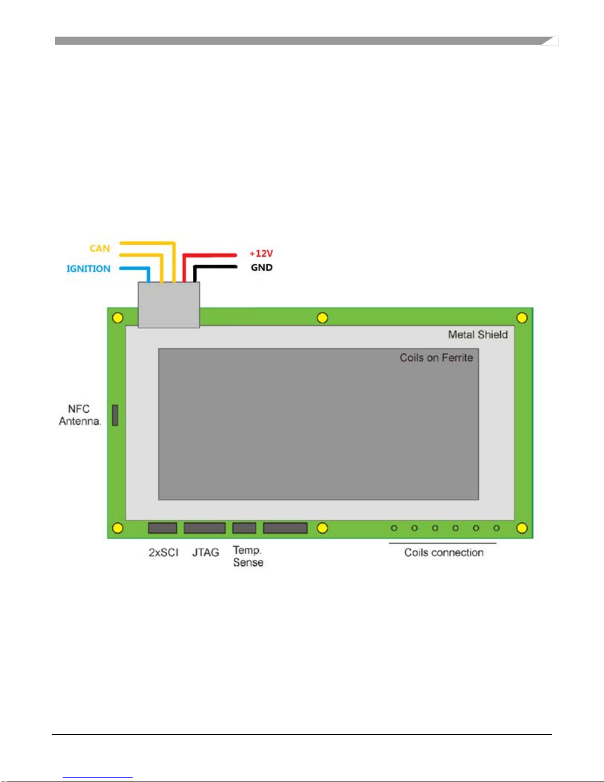
The input connector J1 provides the whole connection to the car wiring. It connects the battery voltage to
the WCT and CAN communication interface.
The input filter consists of the Common Mode Filter FL1 and the filter capacitors C1, C3, C4, C14, and
L1.
The main battery voltage switch is equipped with MOSFET Q1. This stage is controlled by the main
controller WCT1011A/WCT1013A and the IGNITION signal. The hardware overvoltage protection
(more than 20 V DC) is also implemented by D1 and Q2 to this switch.
4.2 System voltage DCDC and LDO
The 12 V Car Battery input is connected to a buck converter U25 (MPQ4558). Its output is 5 V and
supplies LDO U26 (MPQ8904), MOSFET Driver, and CAN Transceiver. The 3.3 V output of LDO is
mainly for WCT1011A/WCT1013A and other 3.3 V powered components.
Generally, the DCDC works at the light-load conditions. High efficiency in light-load is very important
for this auxiliary buck converter.
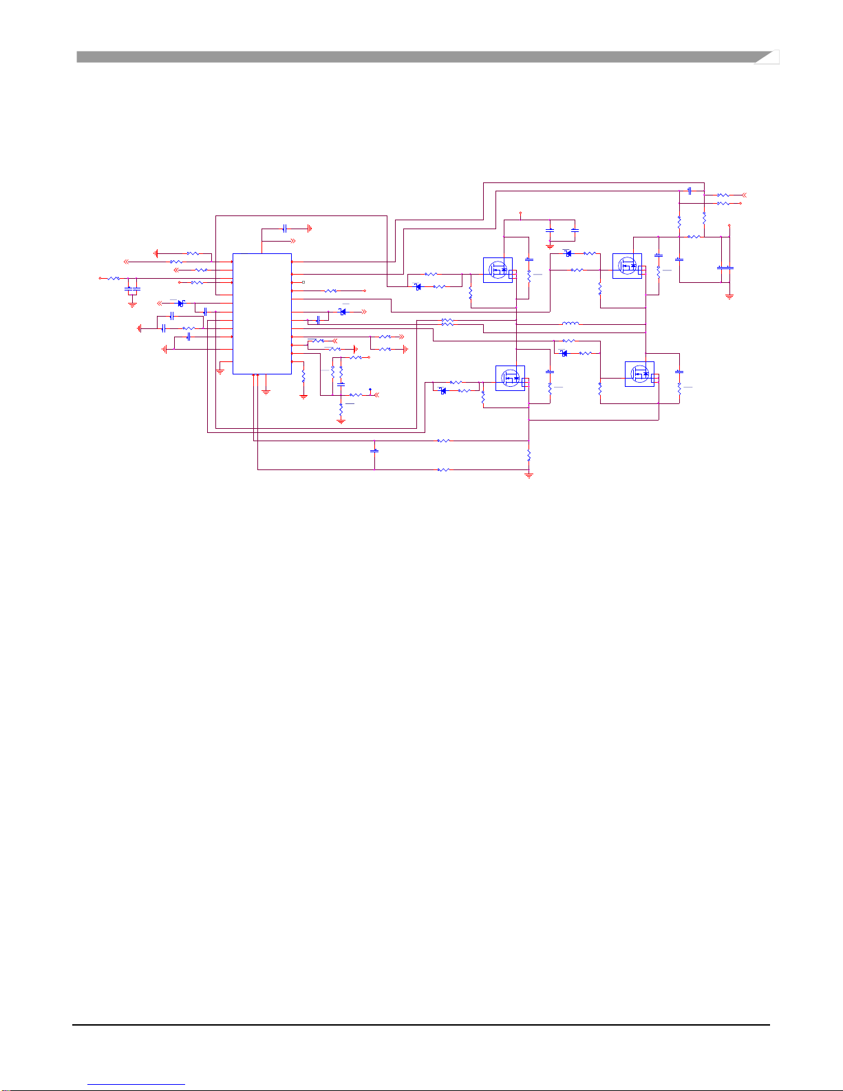
4.3 Rail voltage generated by digital buck-boost or analog buck-boost chip
The Qi specification for the MP-A9 topology requires the DC voltage control to control the power
transferred to the receiver. The buck-boost converter is selected to obtain the regulated DC voltage in the
range from 1 V DC to 24 V DC for the full-bridge inverter power supply. The buck-boost can be digitally
controlled by the WCT chip or the individual analog buck-boost converter and the WCT chip just controls
the output voltage feedback.
Digital buck-boost module includes the drivers, the full-bridge converter, and the output voltage feedback.
The DCDC converter’s control loop is implemented by the firmware, and the control parameters can be
optimized with different main circuit parameters, such as the inductor and output capacitor.
Figure 6 Digital buck-boost main circuits
C371
10uF
C311
0.1uF
50V
VRAIL_2
D84
PMEG060V050EPD
DNP
1
23
GND2
C496
47pF
C368
0.1uF
50V
Ipeak_S2 8
R442
0.015
C449 10uF
C448 10uF
GND2
GND2
GND2
GND2
GND2
GND2
Small board 2
D56
1PS76SB10
A C
D57
1PS76SB10
AC
R400
10.0K
VDriv e_S2
R401
10.0K
C305 0.1uF
C304 0.1uF
R402
10
R403 10
DBUCK_PWML_S2
8
DBUCK_PWMH_S2
8
R404 10
AUIRS2301S
U30
VCC
1
HIN
2
LIN
3
COM
4LO 5
VS 6
HO 7
VB 8
Q51
NVTFS5820NLTAG
1
43
2
5
Q50
NVTFS5820NLTAG
1
43
2
5
Q52
NVTFS5820NLTAG
1
43
2
5
Q53
NVTFS5820NLTAG
1
43
2
5
R405
10.0K
R406
10.0K
VDriv e_S2
C308 0.1uF
R408 10
C307 0.1uF
R407
10
DBOOST_PWML_S2
8
DBOOST_PWMH_S2
8
R409 10
L24
10UH
12
AUIRS2301S
U31
VCC
1
HIN
2
LIN
3
COM
4LO 5
VS 6
HO 7
VB 8
VBAT_SW_2
C369
10uF
R411
3.32
C319
1000pF
C343
1000pF
C344
1000pF
C318
1000pF
R466
3.32
R410
3.32
R467
3.32
WCT1011A/WCT1013A Automotive MP-A9 Wireless Charging Application User’s Guide, Rev. 0, 10/2017
8 NXP Semiconductors