324
AN30182A-EVB
User’s Guide
for Evaluation Board
Revised
Total Pages Page
2013-05-15
Automotive & Industrial Systems Company, Panasonic Corporation
Regulations
No. 1824S02E
Note: The parameters above is subject to change for improvement without notice.
1 Introduction
This user’s guide contains background information for the
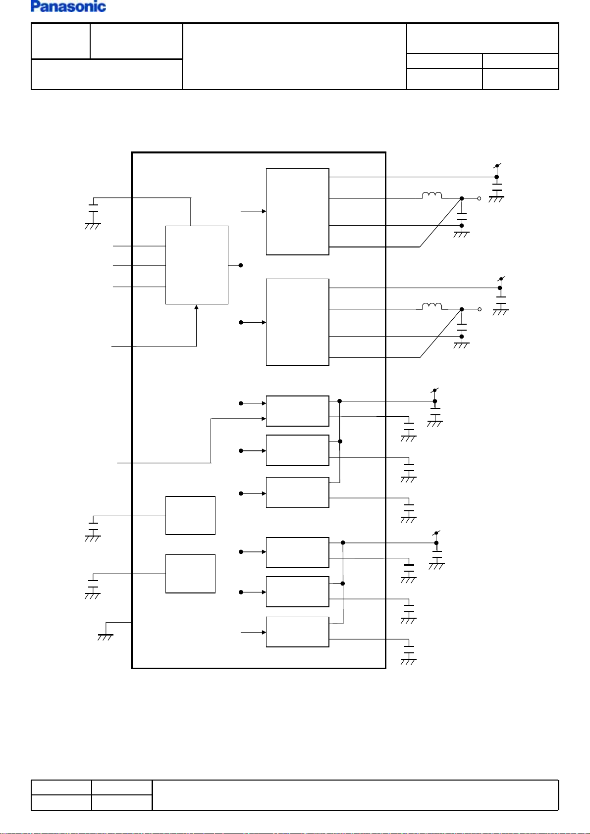
AN30182A : Multi Power Supply (High Efficiency Power LSI)
as well as support documentation for the AN30182A Evaluation Board (AN30182A-EVB). Also included are the schematic, the bill of
materials and the Board Layout for the Evaluation Board.
1.1 Overview
AN30182A is a multi power supply LSI which has high-speed response DC-DC Step Down Regulators (2-ch) and LDO Regulators
(6-ch).
The output DC of each power supply is variable by I2C control.
1.2 Features
—DC-DC Step Down Regulator 2-ch (Output voltage 0.8 V to 2.4 V, Output current 600 mA)
—Regulator 6-ch (Output voltage 1.0 V to 3.3 V, Output current 300 mA)
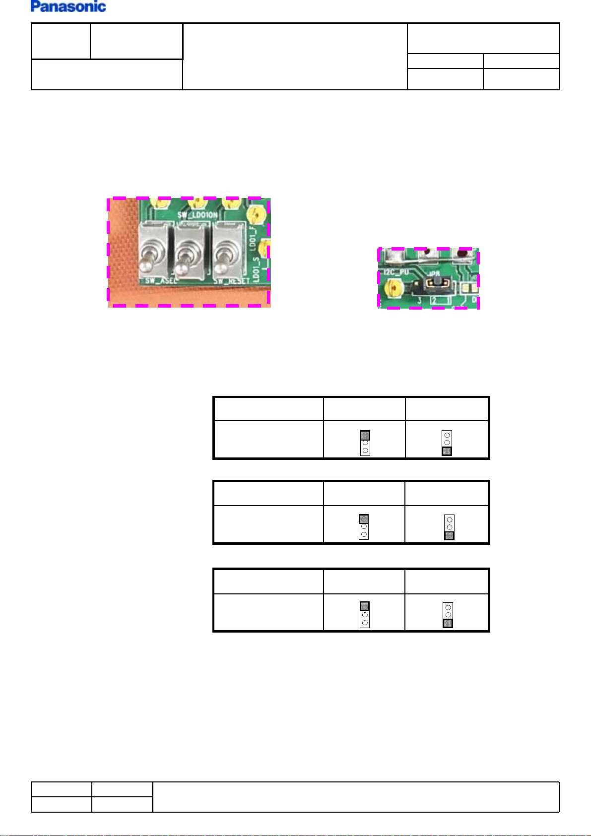
—I2C control (2-slave address selectable)
—Input Voltage Range: VBAT: 2.5V~ 5.5V , DVDD: 1.7V ~ 3.0V
—Built-in Under Voltage Lockout (UVLO), Thermal Shut Down (TSD), Output Over-Current
Protection (OCP), Short-Circuit Protection (SCP) functions
Input voltage and output current range for the evaluation Board are given in Table 1.
1.3 Applications
—Portable appliance, etc
1.4 Package
— 25 pin Wafer Level Chip Size Package (WLCSP)
(Size : 2.15 mm 2.15 mm, 0.4 mm Pitch)
1.5 Type
—Bi-CMOS IC
DC-DC Step Down Regulator: 0.8 V ~ 2.4 V,600 mA
LDO Regulator: 1.0 V ~ 3.3 V,300 mA
Output Current Range
VBAT = 2.5V 〜5.5V
DVDD = 1.7V 〜3.0V
Input Voltage range
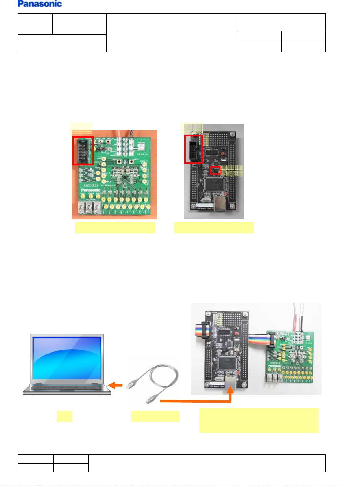
EVB-AN30182A
Evaluation Board
Table 1. Input Voltage and Output Current Summary