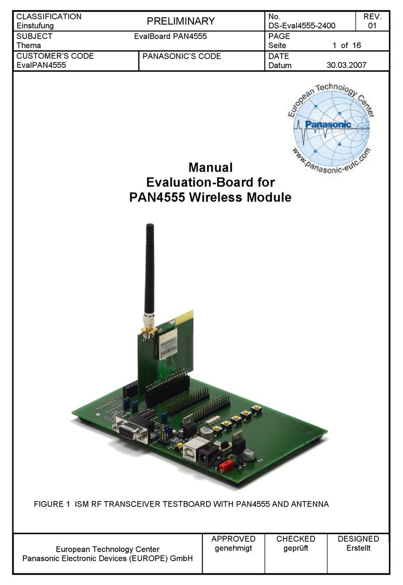
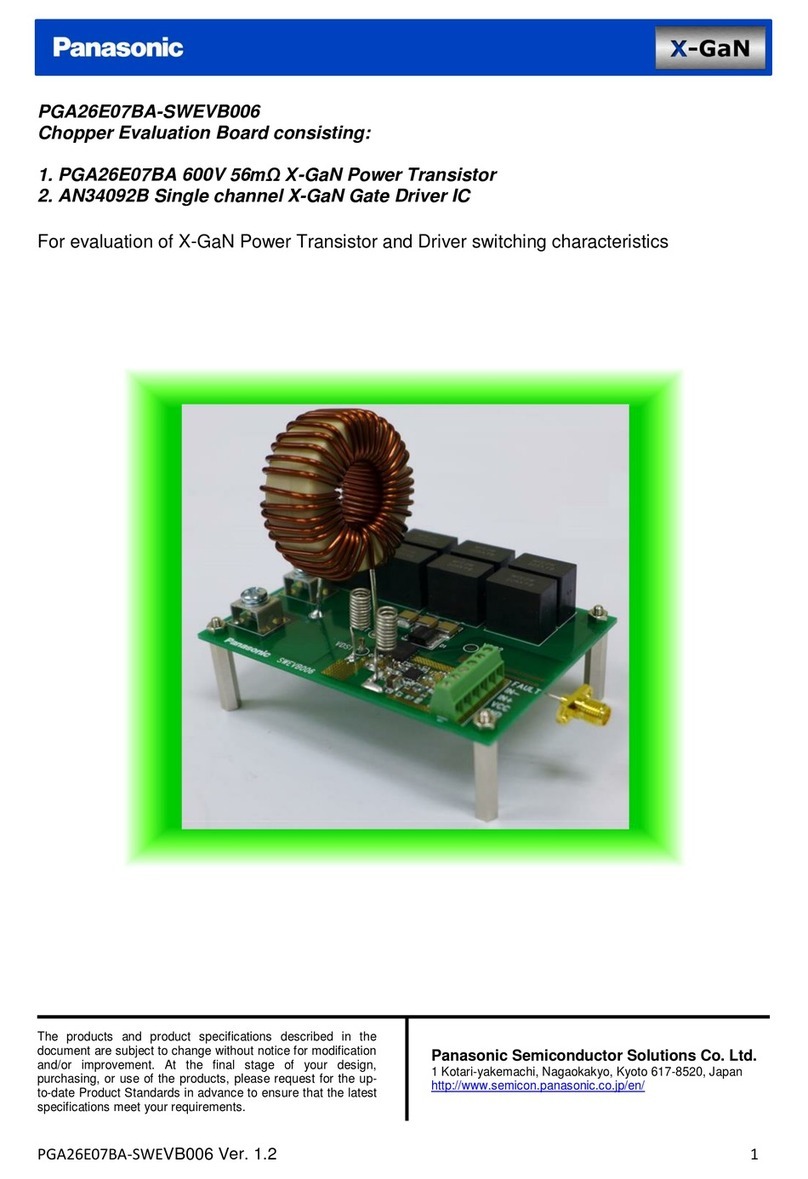
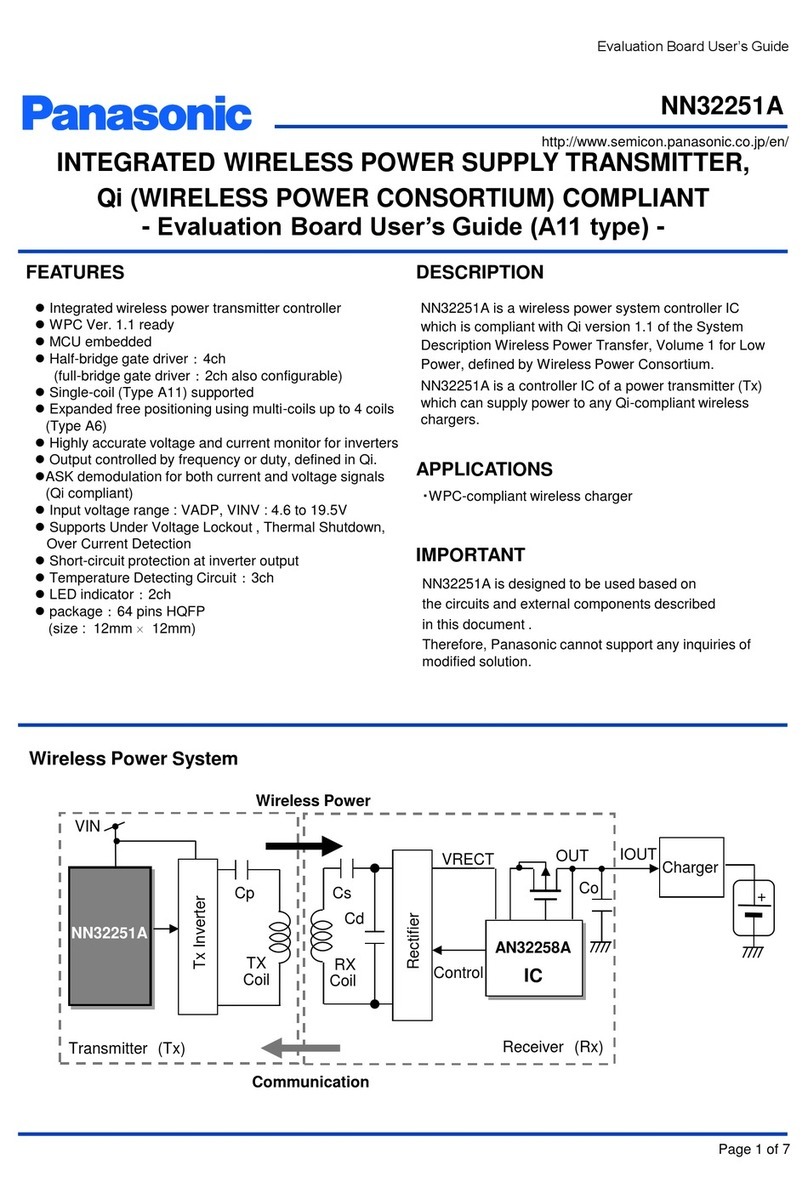
Panasonic PGA26E07BA-SWEVB008 User manual

PGA26E07BA-SWEVB008 Ver. 1.2
PGA26E07BA-SWEVB008
Half Bridge Evaluation Board consisting:
1. PGA26E07BA 600V 70mΩX-GaN Power Transistor
2. AN34092B Single channel X-GaN Gate Driver IC
3. General Purpose Half Bridge Isolator
The products and product specifications described in the
document are subject to change without notice for modification
and/or improvement. At the final stage of your design,
purchasing, or use of the products, please request for the up-to-
date Product Standards in advance to ensure that the latest
specifications meet your requirements.
Panasonic Semiconductor Solutions Co. Ltd.
1 Kotari-yakemachi, Nagaokakyo, Kyoto 617-8520, Japan
http://www.semicon.panasonic.co.jp/en/
The products and product specifications described in
the document are subject to change without notice for modification
and/or improvement. At the final stage of your design, purchasing,
or use of the products, therefore, ask for the most up-to-date
Product Standards in advance to make sure that the latest
specifications satisfy your requirements.
As of March, 2017
Panasonic Industrial Devices
Sales Company of America
Two Riverfront Plaza, 7th Floor
Newark, NJ, 07102, United States
800-344-2112
na.industrial.panasonic.com
Panasonic
Semiconductor Solutions Co., Ltd.
1 Kotari-yakemachi, Nagaokakyo,
Kyoto 617-8520, Japan
Tel. +81-75-951-8151
http://www.semicon.panasonic.co.jp/en
PGA26E07BA-SWEVB008 Ver. 1.2 2
Contents
Features............................................................................................................................................................. 3
Description of the Evaluation board.................................................................................................................. 4
Recommended Operating Conditions............................................................................................................... 5
Schematic Diagram............................................................................................................................................ 6
- Schematic Diagram of optional parts.......................................................................................................... 7
Bill of Materials.................................................................................................................................................. 8
PCB Layout....................................................................................................................................................... 10
Test circuits...................................................................................................................................................... 11
- Slew rate test circuit.................................................................................................................................. 11
- Switching loss test circuit .......................................................................................................................... 12
- Dead time circuit ....................................................................................................................................... 12
- Efficiency test circuit ................................................................................................................................. 13
Equipment ....................................................................................................................................................... 14
Measurement Procedures............................................................................................................................... 15
Low Side dV/dT test......................................................................................................................................... 18
High Side dV/dT test........................................................................................................................................ 20
Low Side Switching Loss test ........................................................................................................................... 22
Efficiency test .................................................................................................................................................. 24
Thermal Profile................................................................................................................................................ 25
Thermal Cooling............................................................................................................................................... 26
Important Notice............................................................................................................................................. 27

PGA26E07BA-SWEVB008 Ver. 1.2 3
Features
Figure 1A: PGA26E07BA-SWEVB008 Board Photo
X-GaN Transistor
█Blocking Voltage: 600V
█Pulse Peak IDS: 61A
█IDS (cont): 26A
█RDS(on) max: 70mΩ
█Normally Off Device
X-GaN Gate Driver
█Supports high switching frequency (~4MHz)
█Achieved safe operation by negative voltage
source and active miller clamp
█Facilitate gate drive design with high
precision gate current source
Source2Source1
Source
Drain
Gate
PGA26E07BA
AN34092B
Propagation
Delay
30ns
D
D
D
D
G
S1
S2
S2
S2

PGA26E07BA-SWEVB008 Ver. 1.2 4
Description of the Evaluation board
PGA26E07BA-SWEVB008 Figure 1A is a complete Half bridge power circuit featuring Panasonic High
Efficiency 600V 70mΩX-GaN transistor in 8X8 SMD package and Panasonic own X-GaN driver AN34092B.
The SWEVB008 provides the flexibility to be configured easily to Buck, Boost, Half bridge and Full bridge
power circuit topology.
Shown in Figure 1A, High / Low side Isolated DCDC module provide the necessary bias of the gate drivers
IC1 and IC2. The isolation of these modules are more than 3000V. SMA2 is a connector for measuring the
VGS of the low side device QA. J1 jumper is for disconnecting the high side DCDC isolated power supply when
operating the half bridge circuit with bootstrap bias. DBS fast recovery diode and RBS provides the bootstrap
bias. IC5 is Silicon Lab 2 input half bridge isolator/general purpose driver Si8275GB. Inputs for the half bridge
isolator driver are IN_L, IN_H and EN. There is an LED mounted on the board to indicate EN input is high.
Typical Voltage for EN pin is 3.3V-5.5V. SWEVB008 can also be modified to use single input PWM
isolator/general purpose driver e.g. Si8274GB.
The evaluation board offers a general platform for testing and developing power circuits using high efficiency
X-GaN in half bridge or full bridge configuration. Figure 1B shows the basic block diagram of this board. The
power loop is made up of QB and QA (GaN-Tr devices), C2, C3, C1 and RS. C2 and C3 are high frequency
bypass capacitors. C1 is the DC link capacitor. RS 47mΩ resistor is use for measuring the IDS flowing through
QA device. X-GaN drivers IC1 and IC2 provides the correct driving voltage and precise current to safely drive
the output transistors QB and QA.
Figure 1B: Block diagram

PGA26E07BA-SWEVB008 Ver. 1.2 5
Recommended Operating Conditions
Table 1 shows the operating conditions used to achieve the switching performance reported in this evaluation
manual. All the components used in the evaluation board are rated for the recommended operating conditions
only.
Please read the measurement procedure before starting the evaluation. It is necessary to refer to the X-GaN
transistor and X-GaN driver datasheet when using this user’s guide. The detailed operation of the gate driver
IC and the design of its peripheral components are described in the OPERATION section of the datasheet.
Table 1: Recommended operating conditions
Parameter
Condition
Input voltage (DC Power ①)
100V-400V
Maximum Rated Power *
800W
Driver IC power supply voltage (DC Power ③)
12V
Driver IC power supply for input stage and External clock
voltage (DC Power ②)
3.3-5.5V
External clock
(pulse generator input) dV/dT Tests
Double pulse
External clock frequency (Duty Cycle)
(pulse generator input) Continuous Pulse Tests
50kHz-200kHz (20%-80%)
External inductor
100uH-360uH @ DC Current>18A
Room Temperature
25ºC
①②③ Power supply equipment number as illustrated in page 18, 20 and 22
* Using attached heatsink

PGA26E07BA-SWEVB008 Ver. 1.2 6
Schematic Diagram
Refer to Figure 2 and 3 below for the circuit schematic of the evaluation board.
Figure 2: SWEVB008 Schematic
* Not populated

PGA26E07BA-SWEVB008 Ver. 1.2 7
- Schematic Diagram of optional parts
Figure 3: Schematic for optional isolated DCDC power supply and Optoisolator

PGA26E07BA-SWEVB008 Ver. 1.2 8
Bill of Materials Table 2: Bill of Materials
Parts
Symbol
Specification
Part Number
Manufacturer
Package
Chip
Resistor
RA1,RB1
15Ω
ERJ-6ENF15R0V
Panasonic
SMD2012
RA2, RB2
0Ω
ERJ-6GEY0R00V
Panasonic
SMD2012
RA3,RB3
1Ω
ERJ-6ENF1R0V
Panasonic
SMD2012
RA4,RB4
-
N.M.
-
SMD1608
RA5,RB5
39kΩ
ERJ-3GEYJ393V
Panasonic
SMD1608
RA6,RB6
**
Bleeder Resistor
-
SMD1608
RA7,RB7
0Ω
ERJ-3GEY0R00V
Panasonic
SMD1608
RA8,RB8
51Ω
ERJ-3GEYJ510V
Panasonic
SMD2012
RA9,RB9
3kΩ
N.M.
-
SMD2012
RBS
-
Bootstrap resistor
-
SMD3216
RLED
1.8 kΩ
ERJ-3GEYJ182V
Panasonic
SMD1608
RLO/RHI
10kΩ
ERJ-3GEYJ103V
Panasonic
SMD1608
Chip
Capacitor
C1
5uF/630V
B32674D6505K000
TDK
Axial
C2,C3
0.1uF/1000V
GRM55DR72J104KW90L
Murata
SMD5750
C4
4.7uF/10V
GRM21BR71A475KA73K
Murata
SMD2012
C5
0.1uF/50V
GRM155R61H104KE14D
Murata
SMD1608
CA1,CB1
2.2uF/25V
GRM31MR71E225KA93L
Murata
SMD3216
CA2,CB2
2.2uF/25V
GRM31MR71E225KA93L
Murata
SMD2012
CA3,CB3
2.2nF/50V
GRM2165C1H222JA01D
Murata
SMD2012
CA4,CB4
0.22uF/25V
GRM155R61E224KE01D
Murata
SMD1608
CA5,CB5
0.47uF/25V
GRM188R71E474KA12D
Murata
SMD1608
CA6,CB6
4.7uF/16V
GRM21BR71C475KA73L
Murata
SMD1608
CA7,CB7
1uF/16V
GRM21BR71C105KA01L
Murata
SMD1608
CA8,CB8
4.7uF/25V
GRM21BR71E475KA73L
Murata
SMD2012
CA9,CB9
100pF/50V
GRM0335C1H101GA01D
Murata
SMD1608
CA10,CB10
-
N.M.
-
SMD1608
CA11,CB11
10uF/25V
GRM32DR71E106KA12L
Murata
SMD3216
CA12,CB12
47pF/50V
GRM0335C1H470JA01D
Murata
SMD1608
CA14,CB14
22uF/25V
GRM32ER71E226KE15L
Murata
SMD3225
**RA6 and RB6 are bleeder resistors but a 0.1uF/50V decoupling cap is mounted instead

PGA26E07BA-SWEVB008 Ver. 1.2 9
- Bill of Materials continued
Parts
Symbol
Specification
Part Number
Manufacturer
Package
Shunt resistor
RS
47mΩ
RL7520WT-R047-F
SUSUMU
SMD3008
Rectifier Diode
DBS
600V / 1A
ES1J
Fairchild
DO-214AC
LED
LED
Gen purpose
SMD LED
LNJ826W86RA
Panasonic
SMD
Screw Terminal
VPN,VS,
LX
-
8174
Keystone
Thru Hole
Terminal Block
CN1
-
1727052
Phoenix Contact
Pitch: 3.81mm
Terminal Block
CN2,CN3
-
1727010
Phoenix Contact
Pitch: 3.54mm
SMA connector
Semi-rigid
-
SMA(PJ)-X-UT47-63
APEX
Technology
-
SMA connector
SMA2
-
19-46-2-TGG
Multicomp
SMD
Isolated DCDC
IC6,IC7
12Vin / 12Vout
MEJ2S1212SC
R12P212S
Murata
SIP(7)
Isolator
IC5
2 Input Half
bridge iso/driver
Si8275GB
SiLab
SOIC-16
GaN Transistor
QA,QB
600V / 70 mΩ
PGA26E07BA
Panasonic
SMD (8mm x
8mm)
Gate Driver
IC1,IC2
gate driver
AN34092B
Panasonic
QFN16
Table 3: Additional Parts use if Si8274 Isolator is used (single input version of SWEVB008)
Parts
Symbol
Specification
Part Number
Manufacturer
Package
Chip Resistor
RDT
51kΩ
ERJ-3GEYJ513V
Panasonic
SMD1608
R0
0Ω
ERJ-3GEY0R00V
Panasonic
SMD1608
Chip Capacitor
C6
100pF/50V
GRM0335C1H101GA01D
Murata
SMD1608
Inverter
IC8
Single inverter
SN74LVC1G04
TI
SOT-23
Isolator
IC5
1 Input Half
bridge
iso/driver
Si8274GB
SiLab
SOIC-16

PGA26E07BA-SWEVB008 Ver. 1.2 10
PCB Layout
PCB Specifications:
Double-sided
Size: 82mm × 122mm
Copper thickness: 70um
Board thickness: 1.6mm
Figure 4: Top and Bottom PCB Layout

PGA26E07BA-SWEVB008 Ver. 1.2 11
Test circuits
- Slew rate test circuit
Figure 5: Low Side slew rate Test circuit
When the inductor L1 is connected between VPN and LX, boost configuration is formed (also refer as low
side test). The low side GaN transistor QA is active in boost mode. The pulses generated by dead time
circuit to drive isolator SI8275GB must not be overlapping. This is to prevent both QA and QB turn on at the
same time and the shoot-through current could damage the circuit.
Figure 6: High Side slew rate Test circuit
When the inductor L1 is connected between LX and VS, buck configuration is formed (also refer as high side
test). Please note that the output connection of the dead time circuit is changed accordingly so the high side
GaN transistor QB acts as active power switch in buck mode.

PGA26E07BA-SWEVB008 Ver. 1.2 12
- Switching loss test circuit
Inductor L1 is connected between VPN and LX, same as low side dV/dT test. The VDS connection is between
QA Drain and Source2 pin. The VGS is not monitored to avoid shorting the Source1 and Source2 pin of the
GaN device QA. The voltage across RS is measured by connecting an SMA cable to a 50 ohm terminated
channel of the oscilloscope. Loss Test procedure is explained further in page 17.
- Dead time circuit
Dead time circuit is required to ensure both GaN transistor QA and QB do not turn ON at the same time. Figure
8 shows a simple example of dead time adjustment circuit. The phasing of inverting and non-inverting outputs
can be fine-tuned by adjusting resistor R1. XOR1 and XOR4 logic gate produce compliment of the input signal.
XOR2 and XOR3 logic gate output the signals with the delay time. The delay times can be set by adjusting the
passive components R2 and R3.
Figure 8: Dead Time Circuit
Figure 7: Low Side Loss Test circuit

PGA26E07BA-SWEVB008 Ver. 1.2 13
- Efficiency test circuit
Figure 9 Shows SWEVB008 in DCDC synchronous boost with bootstrap high side bias circuit. The high side
Isolated DCDC was disconnected by removing the jumper JP. Bootstrap bias circuit is possible because of
the fix duty of 50%. The bootstrap resistor, RBS, is set to 0.5Ω for 100 kHz operation. For higher frequency
operation, do consider reducing the resistance or adopting an isolated DC-DC as shown in Figure 10. The
bootstrap resistor is not mounted on the board.
Figure 9 Circuit for efficiency test with high side circuit powered by bootstrap diode circuit.
Figure 10 Circuit for efficiency test with high side circuit powered by isolated DCDC.

PGA26E07BA-SWEVB008 Ver. 1.2 14
Equipment
The equipment used in the evaluation test circuits is shown in Table 4. This is for reference only.
Table 4: List of Equipment used
No.
Equipment
Specifications
Suggested Model
1
DC Power ①
1 OUTPUT
DC 600V 700W
Keysight N5752A
2
DC Power ②③
2 OUTPUT
DC18V 1.5A
Kenwood PW18-3
3
Pulse Generator
-
Agilent 33250A
4
Dead time circuit
-
General purpose / Basic dead time circuit 100ns
5
Power meter
3 channel power meter
Yokogawa WT500
6
Electronic Load
450V/4.5kW
Chroma 63804
7
Oscilloscope
-
Tektronix DPO7104C
8
Probe
-
TCP0030 Current Probe (IL)
-
P6139B Voltage Probe (VDS, VGS)
-
P5205A Differential Voltage Probe (VDS)
-
BNC to SMA Cable (VRS)

PGA26E07BA-SWEVB008 Ver. 1.2 15
Table 5: Double Pulse Setting with L=320uH
Measurement Procedures
1) Slew Rate dV/dT tests
Initial steps:
Do all the necessary connection between the evaluation board,
components and equipment.
Connect DC power ①to VPN and VS of the board with
the screw terminal block.
Connect deadtime circuit to the IN_H, IN_L, VDD, EN and
GND terminal of the board. Please note that the connection of
dead time circuit to the IN_H and IN_L depending on low side
test or high side test (please refer to page 11).
Connect the inductor from VPN to LX for boost mode (low side test)
or connect inductor from LX to VS for buck mode (high side test).
The VDD voltage must be 3.3V-5V, Isolator VDDI voltage range.
Fix the dead time to 100ns.
Connect the dead time generator to a pulse generator.
Connect DC power ②to VDD/GND terminal of the board to3.3/5V.
Connect DC power ③to AUXH+/AUXH-, AUXL+/AUXL- terminal of
the board.
Probe the point where you want to monitor and observe the
waveform using oscilloscope.
Be careful not to short with other parts. It is recommended to use a coil
wire fixture mounted near SMA2 on the evaluation board for VDS monitoring
refer to Figure 11.
Use an SMA to Tektronics probe adaptor as shown in Figure 12.
Start-up:
Set up the Dead time generator circuit with the amplitude 0-5V and having the double pulse profile as
shown below:
Figure 13: Double Pulse
Again, ensure that the pulse generated occurs only in the burst mode. If the pulse is generated
continuously, the transistor will be damaged by high current flows.
Set DC power ②to 5V. LED will glow to indicate EN (Si8275GB Enable pin) is high
Adjust DC power ③to 12V gradually.
Check VGS waveform when a double pulse is inputted from pulse generator. Ensure to carry out this step
with DC power ①is set to 0V.
Then, the voltage of DC power ①is gradually increased from 0V to predetermined voltage (400V).
Monitor the VDS voltage with oscilloscope and confirm that the VDS voltage rises to the set value.
Input a double pulse with the pulse generator again and check the VGS, VDS and IL waveform.
Observation of waveform will be easier if the trigger is applied at the rising / falling edge of VGS or VDS as
shown on Figure 13 above.
If different inductor value is used other than the suggested, please set the pulse width until the desired IL
value is achieved.
IL
#1
2.5A
2.2µs
5A
4.6µs
7.5A
6.8µs
10A
9.1µs
12.5A
11.1µs
15A
13.1µs
Figure 11: Usage of coil wire
Figure 12: SMA to Probe

PGA26E07BA-SWEVB008 Ver. 1.2 16
Shutdown:
Set the DC power ①slowly to 0V and then follow by the DC power ②and ③to 0V.
Turn off the power. Check the VDS waveform and ensure that the capacitor between VPN and VS terminals
has fully discharged. There is risk of electric shock due to the residual charge.
Measurement of dV/dt for Turn On/Off Switching Characteristics:
The range used is 10%~90%
IL condition is set at 2.5A / 5A / 7.5A / 10A / 12.5A/ 15A with 16 times averaging
Therefore, the dv/dt at turn on: 320V / T-on and the dv/dt at turn off: 320V / T-off
VDS dV/dT measurement during Low side device (QA) testing
Figure 14: Measurement points for Low side device
VDS dV/dT measurement during High side device (QB) testing
Figure 15: Measurement points for High side device
T-on
400V
0V
40V
360V
VDS at
Turn On
VDS at
Turn Off
T-off
T-off
400V
0V
40V
360V
VDS at
Turn Off
VDS at
Turn On
T-on

PGA26E07BA-SWEVB008 Ver. 1.2 17
2) Switching Loss
Initial steps:
Do all the necessary connection between the evaluation board, components and equipment.
Connect DC power ①to VPN and VS of the board with the screw terminal block.
Connect dead time circuit to the IN_H, IN_L, VDD, EN and GND terminal of the board. The loss test is
done in boost mode (low side test). Therefore, Inductor is connected from VPN to LX.
The VDD voltage must be the same as the Isolator VDD voltage. Fix the dead time to 100ns.
Connect the dead time generator to a pulse generator.
Probe the point where you want to monitor and observe the waveform using oscilloscope.
Be careful not to short with other parts. Use the coil wire fixture mounted on the evaluation board for VDS
and IL monitoring.
Use the semi-rigid to monitor VRS waveform. Use the Math Function on the oscilloscope to get
IDS waveform. IDS = VRS /RS. RS is 47mΩ as shown in the BOM List (page 9).
Use the math function on oscilloscope to find the multiplication of VDS and IDS, then use the
measure function on the oscilloscope to find the area under the curve (power loss). See Figure 16.
Figure 16: Power Loss measurement waveform
Start-up:
Set up the Dead time generator circuit with the amplitude 0-5V and having the double pulse profile as
shown in the Figure 13.
Again, ensure that the pulse generated occurs only in the burst mode. If the pulse is generated
continuously, the transistor will be damaged by high current flows.
Set the DC power ②to 5V gradually. Set the DC power ③to 12V gradually.
Check VGS waveform when a double pulse is inputted from pulse generator. Please carry out this step
with DC power ①is set to 0V.
Then, the voltage of DC power ①is gradually increased from 0V to predetermined voltage (400V).
Monitor the VDS voltage with oscilloscope and confirm that the VDS voltage rises to the set value.
Input a double pulse with the pulse generator again and check the VGS, VDS, IDS and power loss (area
under the curve for multiplication of VDS and IDS) waveform.
Observation of waveform will be easier if the trigger is applied at the rising / falling edge of VGS or VDS as
shown on Figure 16 above.
If different inductor value is used other than the one provided, please set the pulse width until the desired
IL value is achieved.
Shutdown:
Set the DC power ①slowly to 0V and then follow by the DC power ②and ③to 0V.
Turn off the power. Check the VDS waveform and ensure that the capacitor between VPN and VS terminals
has fully discharged. There is risk of electric shock due to the residual charge.
QA VDS
QA IDS
Power Loss
(Turn On)

PGA26E07BA-SWEVB008 Ver. 1.2 18
Low Side dV/dT test
Figure 17 shows all the necessary connections for Low Side GaN device (QA) dV/dT testing. Figure 18 shows
the evaluation test circuit. Please refer to pages 15-16 for evaluation procedures.
Figure 17: Connection for Low Side GaN testing
Figure 18: Evaluation Schematic for Low side GaN test
AUXH+
AUXH-
VPN
AUXL-
AUXL+
VDD
INH
GND
EN
GND
IN_L
VS
LX
320uH
Inductor Dead
Time
Circuit
N5752A DC POWER ①PW18-3
DC power ②③
5V
12V
SMA to probe Adapter 33250A

PGA26E07BA-SWEVB008 Ver. 1.2 19
Switching Characteristics Result:
Condition: VPN=400V, VAUXH, VAUXL=12V, (Rgon) RA1,RB1=15/47/100Ω, RA2,RB2=0Ω, RA3,RB3=1Ω, CA3,CB3=2.2nF
I. Low side device (QA) dV/dt Measurement Data
Figure 19: dV/dT at turn off for QA Figure 20: dV/dT at turn on for QA
II. VGS, VDS and IDS Measurement Waveform with (Rgon) RA1,RB1=15Ω
VPN=400V, IDS=2.5A
VPN=400V, IDS=15A
Turn
ON
dV/dt = -83.8[V/ns]
dV/dt= -64.8[V/ns]
Turn
OFF
dV/dt= 10.2[V/ns]
dV/dt= 67.5 [V/ns]
VGS 4V/div
IL 5A/div
VDS 100V/div
Time scale:20ns/div
5GS/s
VGS 4V/div
IL 5A/div
VDS 100V/div
Time scale:20ns/div
5GS/s
VGS 4V/div
IL 5A/div
VDS 100V/div
Time scale:20ns/div
5GS/s
VGS 4V/div
IL 5A/div
VDS 100V/div
Time scale:20ns/div
5GS/s
Important Note: The data presented is meant to demonstrate the high switching capability of Panasonic X-GaN.
The dV/dT data is for reference use only and measured data maybe different depending on evaluation environment.
Figure 21: QA turn on/off waveforms at IDS=2.5A
Figure 22: QA turn on/off waveforms at IDS=15A

PGA26E07BA-SWEVB008 Ver. 1.2 20
Figure 23: Connection for High side GaN test
High Side dV/dT test
Figure 23 shows all the necessary connections for High Side GaN device (QB) dV/dT testing. Figure 24 shows
the evaluation test circuit. Please refer to pages 15-16 for evaluation procedures.
Figure 24: Evaluation schematic for High side GaN test
Table of contents
Other Panasonic Motherboard manuals

Panasonic
Panasonic PGA26E07BA-SWEVB006 User manual

Panasonic
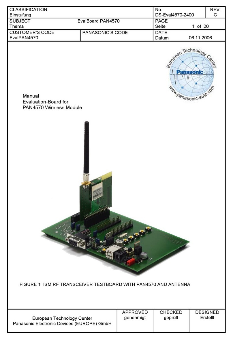
Panasonic PAN4570 User manual

Panasonic
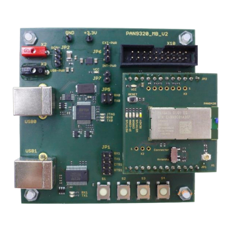
Panasonic PAN9320ETU User manual

Panasonic
Panasonic EVB-NN30312A User manual

Panasonic
Panasonic PAN9520 User manual

Panasonic
Panasonic EvalBoard PAN4555 User manual

Panasonic
Panasonic PAN9420 User manual

Panasonic
Panasonic PAN1311/21 USB User manual

Panasonic
Panasonic Grid-EYE User manual

Panasonic
Panasonic AN30182A-EVB User manual